Sign In
Upload
Manuals
Brands
Altera Manuals
Microcontrollers
Cyclone V
Altera Cyclone V Manuals
Manuals and User Guides for Altera Cyclone V. We have
5
Altera Cyclone V manuals available for free PDF download: Technical Reference, Device Handbook, User Manual, Reference Manual, Boot Manual
Altera Cyclone V Technical Reference (3536 pages)
Hard Processor System
Brand:
Altera
| Category:
Computer Hardware
| Size: 24.75 MB
Table of Contents
Table of Contents
2
Introduction to the Hard Processor System
17
Features of the HPS
19
HPS Block Diagram and System Integration
20
HPS Block Diagram
20
Cortex-A9 Mpcore
21
HPS Interfaces
21
System Interconnect
22
On-Chip Memory
23
Flash Memory Controllers
24
Support Peripherals
25
Interface Peripherals
27
Coresight Debug and Trace
30
Endian Support
31
Introduction to the Hard Processor System Address Map
31
HPS Address Spaces
31
HPS Peripheral Region Address Map
33
Document Revision History
36
Clock Manager
38
Features of the Clock Manager
38
Clock Manager Block Diagram and System Integration
39
L4 Peripheral Clocks
40
Functional Description of the Clock Manager
41
Clock Manager Building Blocks
41
Hardware-Managed and Software-Managed Clocks
44
Clock Groups
44
Resets
54
Safe Mode
54
Interrupts
55
Clock Usage by Module
55
Clock Manager Address Map and Register Definitions
60
Clock Manager Module Address Map
61
Document Revision History
110
Reset Manager
112
Reset Manager Block Diagram and System Integration
113
HPS External Reset Sources
114
Reset Controller
115
Module Reset Signals
116
Slave Interface and Status Register
121
Functional Description of the Reset Manager
121
Reset Sequencing
122
Reset Pins
126
Reset Effects
126
Altering Warm Reset System Response
126
Reset Handshaking
127
Reset Manager Address Map and Register Definitions
127
Reset Manager Module Address Map
128
Document Revision History
143
FPGA Manager
144
Features of the FPGA Manager
144
FPGA Manager Block Diagram and System Integration
145
Functional Description of the FPGA Manager
146
FPGA Manager Building Blocks
146
FPGA Configuration
147
FPGA Status
151
Error Message Extraction
151
Boot Handshake
151
General Purpose I/O
152
Clock
152
Reset
152
FPGA Manager Address Map and Register Definitions
152
FPGA Manager Module Configuration Data Address Map
152
FPGA Manager Module Address Map
153
Document Revision History
194
System Manager
195
Features of the System Manager
195
System Manager Block Diagram and System Integration
196
Functional Description of the System Manager
197
Boot Configuration and System Information
197
Additional Module Control
197
Dma Controller
198
Boot ROM Code
200
FPGA Interface Enables
202
ECC and Parity Control
202
Preloader Handoff Information
203
Clocks
203
Resets
203
System Manager Address Map and Register Definitions
203
Document Revision History
431
Scan Manager
433
Features of the Scan Manager
433
Scan Manager Block Diagram and System Integration
434
ARM JTAG-AP Scan Chains
435
Functional Description of the Scan Manager
437
Communicating with the JTAG TAP Controller
438
Clocks
439
Resets
440
Scan Manager Module Registers Address Map
441
Document Revision History
448
System Interconnect
449
Features of the System Interconnect
449
System Interconnect Block Diagram and System Integration
450
Main Connectivity Matrix
451
Functional Description of the Interconnect
452
System Interconnect Address Spaces
453
Master Caching and Buffering Overrides
461
Security
462
Cyclic Dependency Avoidance Schemes
463
System Interconnect Master Properties
464
Interconnect Slave Properties
465
Upsizing Data Width Function
468
Downsizing Data Width Function
469
Lock Support
470
System Interconnect Resets
471
Document Revision History
582
HPS-FPGA Bridges
583
Features of the HPS-FPGA Bridges
583
HPS-FPGA Bridges Block Diagram and System Integration
585
Functional Description of the HPS-FPGA Bridges
586
Functional Description of the HPS-To-FPGA Bridge
601
Functional Description of the Lightweight HPS-To-FPGA Bridge
614
Clocks and Resets
633
Data Width Sizing
635
Document Revision History
636
Cortex-A9 Microprocessor Unit Subsystem
637
Features of the Cortex-A9 MPU Subsystem
637
Cortex-A9 MPU Subsystem Block Diagram and System Integration
638
Cortex-A9 MPU Subsystem Internals
639
Cortex-A9 Mpcore
640
Implementation Details
641
Cortex-A9 Processor
642
Interactive Debugging Features
643
Floating Point Unit
644
Memory Management Unit
645
Performance Monitoring Unit
648
Generic Interrupt Controller
649
Global Timer
661
Snoop Control Unit
662
Accelerator Coherency Port
663
ACP ID Mapper
667
Implementation Details
668
ACP ID Mapper Address Map and Register Definitions
673
L2 Cache
697
CPU Prefetch
704
Event Trace
705
Clocks
706
Cortex-A9 MPU Subsystem Address Map
707
L2 Cache Controller Address Map
708
Document Revision History
709
Coresight Debug and Trace
712
Features of Coresight Debug and Trace
712
Coresight Debug and Trace Block Diagram and System Integration
713
Functional Description of Coresight Debug and Trace
714
Trace Funnel
715
AMBA Trace Bus Replicator
716
Program Trace Macrocell
721
Debug Clocks
724
Debug Resets
725
Coresight Debug and Trace Programming Model
726
STM Channels
727
CTI Trigger Connections to Outside the Debug System
729
Configuring Embedded Cross-Trigger Connections
730
Coresight Debug and Trace Address Map and Register Definitions
732
System Trace Macrocell (STM) Module Address Map
733
MPU Address Map
735
MPU L2 Cache Controller (L2C-310) Module Address Map
736
Document Revision History
737
SDRAM Controller Subsystem
739
Features of the SDRAM Controller Subsystem
739
SDRAM Controller Subsystem Block Diagram
740
SDRAM Controller Memory Options
741
SDRAM Controller Subsystem Interfaces
742
CSR Interface
743
Memory Controller Architecture
744
Multi-Port Front End
745
Single-Port Controller
746
Functional Description of the SDRAM Controller Subsystem
748
MPFE SDRAM Burst Scheduling
751
Single-Port Controller Operation
752
Memory Protection
757
SDRAM Power Management
762
DDR Calibration
763
Resets
764
Initialization
765
FPGA-To-SDRAM Protocol Details
766
SDRAM Controller Subsystem Programming Model
770
HPS Memory Interface Simulation
771
Debugging HPS SDRAM in the Preloader
773
Enabling Simple Memory Test
774
Enabling the Debug Report
775
Writing a Predefined Data Pattern to SDRAM in the Preloader
778
SDRAM Controller Address Map and Register Definitions
779
Document Revision History
815
On-Chip Memory
817
On-Chip RAM
817
Functional Description of the On-Chip RAM
818
Boot ROM
819
On-Chip Memory Address Map and Register Definitions
820
NAND Flash Controller
822
NAND Flash Controller Features
822
NAND Flash Controller Block Diagram and System Integration
823
Functional Description of the NAND Flash Controller
824
Bootstrap Interface
825
Configuration by Host
826
Local Memory Buffer
827
Resets
828
Command Mapping
829
Data DMA
835
NAND Flash Controller Programming Model
842
Basic Flash Programming
843
Flash-Related Special Function Operations
846
NAND Flash Controller Address Map and Register Definitions
854
NAND Flash Controller Module Registers (AXI Slave) Address Map
855
Dma Registers
859
Document Revision History
945
SD/MMC Controller
947
Features of the SD/MMC Controller
947
SD Card Support Matrix
948
MMC Support Matrix
949
SD/MMC Controller Signal Description
950
Functional Description of the SD/MMC Controller
951
Error Detection
980
Clocks
981
Resets
982
Voltage Switching
983
SD/MMC Controller Programming Model
985
Initialization †
987
Controller/Dma/Fifo Buffer Reset Usage
993
Data Transfer Commands
995
Transfer Stop and Abort Commands
1002
Internal DMA Controller Operations
1004
Commands for SDIO Card Devices
1006
CE-ATA Data Transfer Commands
1008
Card Read Threshold
1016
Interrupt and Error Handling
1019
Booting Operation for Emmc and MMC
1020
SD/MMC Controller Address Map and Register Definitions
1030
Document Revision History
1089
Quad SPI Flash Controller
1090
Features of the Quad SPI Flash Controller
1090
Quad SPI Flash Controller Block Diagram and System Integration
1091
Interface Signals
1092
Data Slave Interface
1093
SPI Legacy Mode
1096
Register Slave Interface
1097
DMA Peripheral Request Controller
1098
Arbitration between Direct/Indirect Access Controller and STIG
1099
XIP Mode
1101
Resets
1102
Quad SPI Flash Controller Programming Model
1103
Setting up the Quad SPI Flash Controller
1104
Indirect Read Operation with DMA Enabled
1105
Indirect Write Operation with DMA Enabled
1106
Quad SPI Flash Controller Address Map and Register Definitions
1108
QSPI Flash Controller Module Registers Address Map
1109
QSPI Flash Module Data (AHB Slave) Address Map
1150
DMA Controller
1152
Features of the DMA Controller
1152
DMA Controller Block Diagram and System Integration
1154
AXI Characteristics for a DMA Transfer
1155
Operating States
1156
Initializing the DMAC
1159
Using the Slave Interfaces
1160
Peripheral Request Interface
1161
Using Events and Interrupts
1172
Aborts
1174
Security Usage
1177
Programming Restrictions
1180
Constraints and Limitations of Use
1184
DMA Controller Programming Model
1185
Instructions
1186
Assembler Directives
1201
MFIFO Buffer Usage Overview
1203
DMA Controller Address Map and Register Definitions
1211
Address Map and Register Definitions
1213
Document Revision History
1214
Advertisement
Altera Cyclone V Device Handbook (1077 pages)
Brand:
Altera
| Category:
Computer Hardware
| Size: 7.66 MB
Table of Contents
Volume 1: Device Interfaces and Integration
2
Table of Contents
2
Logic Array Blocks and Adaptive Logic Modules in Cyclone V Devices
10
Lab
10
Mlab
11
Local and Direct Link Interconnects
12
LAB Control Signals
13
ALM Resources
14
ALM Output
15
ALM Operating Modes
16
Normal Mode
17
Extended LUT Mode
17
Arithmetic Mode
17
Shared Arithmetic Mode
18
Normal Mode
18
Document Revision History
20
Embedded Memory Blocks in Cyclone V Devices
21
Types of Embedded Memory
21
Embedded Memory Capacity in Cyclone V Devices
21
Embedded Memory Design Guidelines for Cyclone V Devices
22
Guideline: Consider the Memory Block Selection
22
Guideline: Implement External Conflict Resolution
23
Guideline: Customize Read-During-Write Behavior
23
Guideline: Consider Power-Up State and Memory Initialization
26
Guideline: Control Clocking to Reduce Power Consumption
27
Embedded Memory Features
27
Embedded Memory Configurations
28
Mixed-Width Port Configurations
29
Embedded Memory Modes
30
Embedded Memory Clocking Modes
31
Clocking Modes for each Memory Mode
31
Asynchronous Clears in Clocking Modes
32
Output Read Data in Simultaneous Read/Write
32
Independent Clock Enables in Clocking Modes
33
Parity Bit in Memory Blocks
33
Byte Enable in Embedded Memory Blocks
33
Byte Enable Controls in Memory Blocks
33
Data Byte Output
34
RAM Blocks Operations
35
Memory Blocks Packed Mode Support
35
Memory Blocks Address Clock Enable Support
35
Document Revision History
37
Variable Precision DSP Blocks in Cyclone V Devices
39
Features
39
Supported Operational Modes in Cyclone V Devices
40
Resources
41
Design Considerations
42
Operational Modes
42
Internal Coefficient and Pre-Adder
42
Accumulator
42
Chainout Adder
42
Block Architecture
43
Input Register Bank
44
Pre-Adder
46
Internal Coefficient
46
Multipliers
46
Adder
47
Accumulator and Chainout Adder
47
Systolic Registers
48
Double Accumulation Register
48
Output Register Bank
48
Operational Mode Descriptions
48
Independent Multiplier Mode
49
Independent Complex Multiplier Mode
51
Multiplier Adder Sum Mode
53
18 X 18 Multiplication Summed with 36-Bit Input Mode
53
Systolic FIR Mode
53
Document Revision History
56
Clock Networks and Plls in Cyclone V Devices
58
Clock Networks
58
Clock Resources in Cyclone V Devices
59
Types of Clock Networks
60
Clock Sources Per Quadrant
64
Types of Clock Regions
65
Clock Network Sources
66
Clock Output Connections
68
Clock Control Block
68
Clock Power down
71
Clock Enable Signals
71
Cyclone V Plls
73
PLL Physical Counters in Cyclone V Devices
73
PLL Locations in Cyclone V Devices
74
PLL Migration Guidelines
79
Fractional PLL Architecture
79
PLL Cascading
80
PLL External Clock I/O Pins
80
PLL Control Signals
81
Clock Feedback Modes
82
Clock Multiplication and Division
88
Programmable Phase Shift
89
Programmable Duty Cycle
89
Clock Switchover
89
PLL Reconfiguration and Dynamic Phase Shift
94
Document Revision History
95
I/O Features in Cyclone V Devices
98
I/O Resources Per Package for Cyclone V Devices
98
I/O Vertical Migration for Cyclone V Devices
101
Verifying Pin Migration Compatibility
102
I/O Standards Support in Cyclone V Devices
102
I/O Standards Support for FPGA I/O in Cyclone V Devices
102
I/O Standards Support for HPS I/O in Cyclone V Devices
104
I/O Standards Voltage Levels in Cyclone V Devices
105
Multivolt I/O Interface in Cyclone V Devices
107
I/O Design Guidelines for Cyclone V Devices
108
Mixing Voltage-Referenced and Non-Voltage-Referenced I/O Standards
108
Plls and Clocking
109
LVDS Interface with External PLL Mode
112
Guideline: Use the same V
114
CCPD for All I/O Banks in a Group
114
Guideline: Ensure Compatible V
115
CCIO and
115
Ccio Ccpd
115
CCPD Voltage in the same Bank
115
Guideline: VREF Pin Restrictions
115
Guideline: Observe Device Absolute Maximum Rating for 3.3 V Interfacing
115
Guideline: Adhere to the LVDS I/O Restrictions and Differential Pad Placement Rules
116
I/O Banks Locations in Cyclone V Devices
116
I/O Banks Groups in Cyclone V Devices
118
Modular I/O Banks for Cyclone V E Devices
119
Modular I/O Banks for Cyclone V GX Devices
120
Modular I/O Banks for Cyclone V GT Devices
121
Modular I/O Banks for Cyclone V SE Devices
122
Modular I/O Banks for Cyclone V SX Devices
123
Modular I/O Banks for Cyclone V ST Devices
124
I/O Element Structure in Cyclone V Devices
124
I/O Buffer and Registers in Cyclone V Devices
124
Programmable IOE Features in Cyclone V Devices
126
Programmable Current Strength
127
Programmable Output Slew-Rate Control
128
Programmable IOE Delay
128
Programmable Output Buffer Delay
128
Programmable Pre-Emphasis
129
Programmable Differential Output Voltage
129
I/O Pins Features for Cyclone V Devices
130
Open-Drain Output
130
Bus-Hold Circuitry
130
Pull-Up Resistor
131
On-Chip I/O Termination in Cyclone V Devices
131
R SOCT Without Calibration in Cyclone V Devices
131
R SOCT with Calibration in Cyclone V Devices
131
R TOCT with Calibration in Cyclone V Devices
131
Dynamic OCT in Cyclone V Devices
137
LVDS Input R DOCT in Cyclone V Devices
138
OCT Calibration Block in Cyclone V Devices
139
External I/O Termination for Cyclone V Devices
141
Single-Ended I/O Termination
142
Differential I/O Termination
144
Dedicated High-Speed Circuitries
149
High-Speed Differential I/O Locations
150
LVDS SERDES Circuitry
151
True LVDS Buffers in Cyclone V Devices
152
Emulated LVDS Buffers in Cyclone V Devices
160
Differential Transmitter in Cyclone V Devices
160
Transmitter Blocks
160
Serializer Bypass for DDR and SDR Operations
161
Differential Receiver in Cyclone V Devices
162
Receiver Blocks in Cyclone V Devices
162
Receiver Mode in Cyclone V Devices
164
Receiver Clocking for Cyclone V Devices
165
Differential I/O Termination for Cyclone V Devices
165
Source-Synchronous Timing Budget
166
Differential Data Orientation
166
Differential I/O Bit Position
167
Transmitter Channel-To-Channel Skew
168
Receiver Skew Margin for LVDS Mode
168
Document Revision History
170
External Memory Interfaces in Cyclone V Devices
175
External Memory Performance
176
HPS External Memory Performance
176
Memory Interface Pin Support in Cyclone V Devices
176
Guideline: Using DQ/DQS Pins
177
DQ/DQS Bus Mode Pins for Cyclone V Devices
177
DQ/DQS Groups in Cyclone V E
179
DQ/DQS Groups in Cyclone V GX
181
DQ/DQS Groups in Cyclone V GT
183
DQ/DQS Groups in Cyclone V SE
185
DQ/DQS Groups in Cyclone V SX
185
DQ/DQS Groups in Cyclone V ST
186
External Memory Interface Features in Cyclone V Devices
186
Uniphy IP
186
External Memory Interface Datapath
187
DQS Phase-Shift Circuitry
187
PHY Clock (PHYCLK) Networks
195
DQS Logic Block
198
Dynamic OCT Control
200
IOE Registers
200
Delay Chains
202
I/O and DQS Configuration Blocks
203
Hard Memory Controller
204
Features of the Hard Memory Controller
204
Multi-Port Front End
206
Bonding Support
207
Hard Memory Controller Width for Cyclone V E
209
Hard Memory Controller Width for Cyclone V GX
210
Hard Memory Controller Width for Cyclone V GT
211
Hard Memory Controller Width for Cyclone V SE
211
Hard Memory Controller Width for Cyclone V SX
212
Hard Memory Controller Width for Cyclone V ST
212
Document Revision History
213
Configuration, Design Security, and Remote System Upgrades in Cyclone V Devices
216
Enhanced Configuration and Configuration Via Protocol
216
MSEL Pin Settings
217
Configuration Sequence
218
Power up
219
Reset
219
Configuration
219
Configuration Error Handling
220
Initialization
221
User Mode
221
Device Configuration Pins
221
Configuration Pin Options in the Quartus II Software
223
Fast Passive Parallel Configuration
224
Fast Passive Parallel Single-Device Configuration
224
Fast Passive Parallel Multi-Device Configuration
225
Active Serial Configuration
227
DATA Clock (DCLK)
227
Active Serial Single-Device Configuration
228
Active Serial Multi-Device Configuration
229
Estimating the Active Serial Configuration Time
230
Using EPCS and EPCQ Devices
230
Controlling EPCS and EPCQ Devices
231
Trace Length and Loading
231
Programming EPCS and EPCQ Devices
231
Passive Serial Configuration
235
Passive Serial Single-Device Configuration Using an External Host
236
Passive Serial Single-Device Configuration Using an Altera Download Cable
236
Passive Serial Multi-Device Configuration
237
JTAG Configuration
239
JTAG Single-Device Configuration
240
JTAG Multi-Device Configuration
242
CONFIG_IO JTAG Instruction
242
Configuration Data Compression
243
Enabling Compression before Design Compilation
243
Enabling Compression after Design Compilation
243
Using Compression in Multi-Device Configuration
243
Remote System Upgrades
244
Configuration Images
245
Configuration Sequence in the Remote Update Mode
245
Remote System Upgrade Circuitry
246
Enabling Remote System Upgrade Circuitry
246
Remote System Upgrade Registers
247
Remote System Upgrade State Machine
249
User Watchdog Timer
249
Design Security
249
ALTCHIP_ID Megafunction
250
JTAG Secure Mode
250
Security Key Types
251
Security Modes
252
Design Security Implementation Steps
252
Document Revision History
253
SEU Mitigation for Cyclone V Devices
254
Error Detection Features
254
Configuration Error Detection
254
User Mode Error Detection
254
Specifications
255
Minimum EMR Update Interval
255
Error Detection Frequency
256
CRC Calculation Time
256
Using Error Detection Features in User Mode
257
Enabling Error Detection
257
CRC_ERROR Pin
258
Error Detection Registers
258
Error Detection Process
260
Testing the Error Detection Block
261
Document Revision History
262
JTAG Boundary-Scan Testing in Cyclone V Devices
263
BST Operation Control
263
Idcode
263
Supported JTAG Instruction
265
JTAG Secure Mode
268
JTAG Private Instruction
268
I/O Voltage for JTAG Operation
269
Performing BST
269
Enabling and Disabling IEEE Std. 1149.1 BST Circuitry
270
Guidelines for IEEE Std. 1149.1 Boundary-Scan Testing
271
IEEE Std. 1149.1 Boundary-Scan Register
271
Boundary-Scan Cells of a Cyclone V Device I/O Pin
272
Document Revision History
274
Power Management in Cyclone V Devices
275
Power Consumption
275
Dynamic Power Equation
275
Hot-Socketing Feature
276
Hot-Socketing Implementation
276
Power-Up Sequence
278
Power-On Reset Circuitry
279
Power Supplies Monitored and Not Monitored by the por Circuitry
281
Document Revision History
282
Volume 2: Transceivers
284
Transceiver Architecture in Cyclone V Devices
288
Architecture Overview
289
Transceiver Banks
290
6.144 Gbps CPRI Support Capability in GT Devices
295
Transceiver Channel Architecture
295
PMA Architecture
296
Transmitter PMA Datapath
297
Receiver PMA Datapath
302
Transmitter PLL
307
Clock Divider
311
Calibration Block
312
PCS Architecture
314
Transmitter PCS Datapath
315
Receiver PCS Datapath
321
Channel Bonding
336
PLL Sharing
336
Document Revision History
336
Transceiver Clocking in Cyclone V Devices
339
Input Reference Clocking
339
Dedicated Reference Clock Pins
340
Fractional PLL (Fpll)
342
Internal Clocking
343
Transmitter Clock Network
345
Transmitter Clocking
347
Receiver Clocking
352
FPGA Fabric Transceiver Interface Clocking
356
Transceiver Datapath Interface Clocking
359
Transmitter Datapath Interface Clocking
359
Receiver Datapath Interface Clock
363
Document Revision History
366
Transceiver Reset Control in Cyclone V Devices
367
PHY IP Embedded Reset Controller
367
Embedded Reset Controller Signals
367
Resetting the Transceiver with the PHY IP Embedded Reset Controller During Device Power-Up
369
Resetting the Transceiver with the PHY IP Embedded Reset Controller During Device Operation
370
User-Coded Reset Controller
371
User-Coded Reset Controller Signals
372
Resetting the Transmitter with the User-Coded Reset Controller During Device Power-Up
373
Resetting the Transmitter with the User-Coded Reset Controller During Device Operation
374
Resetting the Receiver with the User-Coded Reset Controller During Device Power-Up Configuration
375
Resetting the Receiver with the User-Coded Reset Controller During Device Operation
376
Transceiver Reset Control Signals Using Avalon Memory Map Registers
377
Clock Data Recovery Manual Lock Mode Reset Sequence
378
Control Settings for CDR Manual Lock Mode
378
Resetting the Transceiver in CDR Manual Lock Mode
379
Resetting the Transceiver During Dynamic Reconfiguration
379
Guidelines for Dynamic Reconfiguration if Transmitter Duty Cycle Distortion Calibration Is Required During Device Operation
380
Transceiver Blocks Affected by the Reset and Powerdown Signals
380
Transceiver Power-Down
381
Document Revision History
381
Transceiver Protocol Configurations in Cyclone V Devices
384
PCI Express
384
PIPE Transceiver Datapath
385
Pcie Supported Features
386
Pcie Supported Configurations and Placement Guidelines
389
Gigabit Ethernet
393
Gigabit Ethernet Transceiver Datapath
395
Xaui
398
Transceiver Datapath in a XAUI Configuration
399
XAUI Supported Features
401
Transceiver Clocking and Channel Placement Guidelines in XAUI Configuration
404
Serial Digital Interface
406
Configurations Supported in SDI Mode
407
Serial Digital Interface Transceiver Datapath
408
Serial Data Converter (SDC) JESD204
408
SATA and SAS Protocols
409
Deterministic Latency Protocols-CPRI and OBSAI
411
Latency Uncertainty Removal with the Phase Compensation FIFO in Register Mode
411
Channel PLL Feedback for Deterministic Relationship
411
CPRI and OBSAI
412
6.144-Gbps Support Capability in Cyclone V GT Devices
413
CPRI Enhancements
414
Document Revision History
416
Standard PCS Configuration
418
Custom Configuration Channel Options
419
Rate Match FIFO in Custom Configuration
422
Standard PCS in Low Latency Configuration
423
Low Latency Custom Configuration Channel Options
424
Document Revision History
427
Transceiver Loopback Support
428
Serial Loopback
428
Forward Parallel Loopback
429
PIPE Reverse Parallel Loopback
430
Reverse Serial Loopback
430
Reverse Serial Pre-CDR Loopback
431
Document Revision History
432
Dynamic Reconfiguration in Cyclone V Devices
433
Dynamic Reconfiguration Features
433
Offset Cancellation
434
Transmitter Duty Cycle Distortion Calibration
434
PMA Analog Controls Reconfiguration
435
Dynamic Reconfiguration of Loopback Modes
436
Transceiver PLL Reconfiguration
436
Transceiver Channel Reconfiguration
437
Transceiver Interface Reconfiguration
437
Reduced .Mif Reconfiguration
438
Unsupported Reconfiguration Modes
438
Document Revision History
439
Altera Cyclone V User Manual (136 pages)
Hard IP for PCI Express
Brand:
Altera
| Category:
Motherboard
| Size: 3.95 MB
Table of Contents
Table of Contents
3
Chapter 1. Datasheet
7
Features
7
Release Information
9
Device Family Support
9
Configurations
9
Debug Features
10
IP Core Verification
11
Performance and Resource Utilization
11
Recommended Speed Grades
11
Chapter 2. Getting Started
13
Megawizard Plug-In Manager Design Flow
15
Creating a Quartus II Project
15
Customizing the Endpoint in the Megawizard Plug-In Manager Design Flow
16
Understanding the Files Generated
18
Qsys Design Flow
21
Customizing the Endpoint in Qsys
21
Specifying the Parameters for the Cyclone V Hard IP for PCI Express
22
Specifying the Parameters for the Example Design
24
Completing the Qsys System
25
Generating the Simulation Model Using Qsys
28
Quartus II Compilation
29
Compiling the Design in the Megawizard Plug-In Manager Design Flow
29
Compiling the Design in the Qsys Design Flow
29
Modifying the Example Design
31
Chapter 3. Parameter Settings
33
System Settings
33
Port Functions
35
Parameters Shared Across All Port Functions
35
Device
36
Error Reporting
37
Link
38
Slot
38
Power Management
39
Parameters Defined Separately for All Port Functions
39
Base Address Registers for Function <N
39
Base and Limit Registers for Root Port Func <N
39
Device ID Registers for Function <N
39
PCI Express/Pci Capabilities for Func <N
39
Chapter 4. IP Core Architecture
43
Key Interfaces
44
Avalon-ST Interface
44
RX Datapath
44
TX Datapath
44
Clocks and Reset
45
Local Management Interface (LMI Interface)
45
Interrupts
45
Protocol Layers
46
Transaction Layer
46
Configuration Space
47
Data Link Layer
48
Physical Layer
49
Multi-Function Support
52
Chapter 5. IP Core Interfaces
54
Avalon-ST RX Interface
55
Data Alignment and Timing for the 64-Bit Avalon-ST RX Interface
57
Avalon-ST TX Interface
60
Avalon-ST Packets to PCI Express Tlps
63
Data Alignment and Timing for the 64-Bit Avalon-ST TX Interface
63
Root Port Mode Configuration Requests
65
ECRC Forwarding
66
Clock Signals
66
Reset Signals
66
ECC Error Signals
69
Interrupts for Endpoints
69
Interrupts for Root Ports
70
Completion Side Band Signals
71
Transaction Layer Configuration Space Signals
72
Configuration Space Register Access Timing
75
Configuration Space Register Access
76
LMI Signals
79
LMI Read Operation
81
LMI Write Operation
81
Power Management Signals
82
Physical Layer Interface Signals
84
Transceiver Reconfiguration
84
Serial Interface Signals
84
PIPE Interface Signals
85
Test Signals
88
Advertisement
Altera Cyclone V Reference Manual (66 pages)
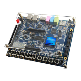
GT FPGA Development Board
Brand:
Altera
| Category:
Motherboard
| Size: 1.77 MB
Table of Contents
Table of Contents
3
Chapter 1. Overview
5
General Description
5
Board Component Blocks
6
Development Board Block Diagram
8
Handling the Board
8
Chapter 2. Board Components
10
Board Overview
10
Featured Device: Cyclone V GT FPGA
13
I/O Resources
13
MAX V CPLD 5M2210 System Controller
14
Configuring the MAX V Device to Program EPCQ
19
FPGA Configuration
19
FPGA Programming over Embedded USB-Blaster
19
FPGA Programming from Flash Memory
21
Using the EPCQ Flash Memory
22
FPGA Programming over External USB-Blaster
23
Status Elements
23
Setup Elements
25
Board Settings DIP Switch
25
JTAG Chain Control or PCI Express Control DIP Switch
26
FPGA Configuration Mode DIP Switch
26
CPU Reset Push Button
26
MAX V Reset Push Button
27
Program Configuration Push Button
27
Program Select Push Button
27
Clock Circuitry
27
On-Board Oscillators
27
Off-Board Clock Input/Output
29
General User Input/Output
30
User-Defined Push Buttons
30
User-Defined DIP Switch
31
User-Defined Leds
31
General Leds
31
HSMC Leds
32
PCI Express Leds
32
Character LCD
33
Components and Interfaces
33
PCI Express
33
10/100/1000 Ethernet
35
Hsmc
37
SDI Channel (Optional)
43
SDI Video Output
44
SDI Video Input
45
Memory
46
Ddr3 Sdram
46
Ddr3A
46
Ddr3B
51
Flash
57
Power Supply
58
Power Distribution System
59
Power Measurement
60
Altera Cyclone V Boot Manual (30 pages)
HPS SoC
Brand:
Altera
| Category:
Microcontrollers
| Size: 1.03 MB
Advertisement
Related Products
Altera Cyclone V GX FPGA
Altera Cyclone V GX Starter Kit
Altera Cyclone V SoC
Altera Cyclone V GT FPGA
Altera Cyclone V E FPGA
Altera Cyclone III FPGA
Altera Cyclone III
Altera Cyclone IV GX FPGA
Altera Cyclone IV
Altera Cyclone IV GX
Altera Categories
Motherboard
Microcontrollers
Computer Hardware
Transceiver
Recording Equipment
More Altera Manuals
Login
Sign In
OR
Sign in with Facebook
Sign in with Google
Upload manual
Upload from disk
Upload from URL