Altera Cyclone V Reference Manual
Gt fpga development board
Hide thumbs
Also See for Cyclone V:
- Technical reference (3536 pages) ,
- Device handbook (1077 pages) ,
- User manual (136 pages)

Related Manuals for Altera Cyclone V


Summary of Contents for Altera Cyclone V
- Page 1 Cyclone V GT FPGA Development Board Reference Manual Cyclone V GT FPGA Development Board Reference Manual 101 Innovation Drive San Jose, CA 95134 www.altera.com MNL-01078-1.3 Feedback Subscribe Arrow.com. Downloaded from...
- Page 2 © 2017 Altera Corporation. All rights reserved. ALTERA, ARRIA, CYCLONE, HARDCOPY, MAX, MEGACORE, NIOS, QUARTUS and STRATIX words and logos are trademarks of Altera Corporation and registered in the U.S. Patent and Trademark Office and in other countries. All other words and logos identified as trademarks or service marks are the property of their respective holders as described at www.altera.com/common/legal.html.
-
Page 3: Table Of Contents
Featured Device: Cyclone V GT FPGA ........ - Page 4 How to Contact Altera ........
-
Page 5: Chapter 1. Overview
The Cyclone V GT FPGA development board provides a hardware platform for developing and prototyping low-power, high-performance, and logic-intensive designs using Altera’s Cyclone V GT FPGA device. The board provides a wide range of peripherals and memory interfaces to facilitate the development of Cyclone V GT designs. -
Page 6: Board Component Blocks
Chapter 1: Overview Board Component Blocks Board Component Blocks The development board features the following major component blocks: ■ One Cyclone V GT FPGA (5CGTFD9E5F35C7N) in a 1152-pin FineLine BGA (FBGA) package ■ FPGA configuration circuitry ® V CPLD (5M2210ZF256C4N) in a 256-pin FBGA package as the System ■... - Page 7 PCI Express edge connector ■ ■ Mechanical PCI Express half-length form factor (4.376" x 6.600") ■ ■ System Monitoring—Power (voltage, current, wattage) August 2017 Altera Corporation Cyclone V GT FPGA Development Board Reference Manual Arrow.com. Arrow.com. Arrow.com. Arrow.com. Arrow.com. Arrow.com. Arrow.com.
-
Page 8: Development Board Block Diagram
Chapter 1: Overview Development Board Block Diagram Development Board Block Diagram Figure 1–1 shows a block diagram of the Cyclone V GT FPGA development board. Figure 1–1. Cyclone V GT FPGA Development Board Block Diagram Resistor Stuffing Option with HSMA... - Page 9 A complete set of schematics, a physical layout database, and fabrication files for the development board reside in the Cyclone V GT FPGA development kit board design files directory.
-
Page 10: Chapter 2. Board Components
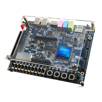
2–2 Chapter 2: Board Components Board Overview Board Overview This section provides an overview of the Cyclone V GT FPGA development board, including an annotated board image and component descriptions. Figure 2–1 shows an overview of the board features. Figure 2–1. Overview of the Cyclone V GT FPGA Development Board Features Table 2–1... - Page 11 125-MHz oscillator 125.000-MHz voltage controlled oscillator for the FPGA. J11, J12 SDI transceiver connectors Drives serial data input/output to or from the SDI video port. August 2017 Altera Corporation Cyclone V GT FPGA Development Board Reference Manual Arrow.com. Arrow.com. Arrow.com. Arrow.com.
- Page 12 DQS/DQx32 assignments for future use. RJ-45 connector which provides a 10/100/1000 Ethernet connection Gigabit Ethernet port via a Marvell 88E1111 PHY and the FPGA-based Altera Triple Speed Ethernet MegaCore function in RGMII mode. Video and Display Ports Connector that interfaces to a provided 16 character × 2 line LCD Character LCD module along with four standoffs.
-
Page 13: Featured Device: Cyclone V Gt Fpga
18-bit × 18-bit Multiplier PLLs Transceivers (6 Gbps) I/O Resources The Cyclone V GT 5CGTFD9E5F35C7N device has total of 560 user I/Os and 12 transceiver channels. Table 2–3 lists the Cyclone V GT device I/O pin count and usage by function on the board. -
Page 14: Max V Cpld 5M2210 System Controller
— Configuration — — Total I/O Used: Table 2–4 lists the Cyclone V GT device transceiver count and usage by function on the board. Table 2–4. Cyclone V GT Transceivers Function Count HSMA port HSMA port or SDI (supports HSMA by default) - Page 15 1.8-V Embedded USB-Blaster II FACTORY command status FACTORY_STATUS 1.8-V DIP switch to load factory or user design at power-up FACTORY_USER August 2017 Altera Corporation Cyclone V GT FPGA Development Board Reference Manual Arrow.com. Arrow.com. Arrow.com. Arrow.com. Arrow.com. Arrow.com. Arrow.com.
- Page 16 FM data bus FM_D2 1.8-V FM data bus FM_D3 1.8-V FM data bus FM_D4 1.8-V FM data bus FM_D5 Cyclone V GT FPGA Development Board August 2017 Altera Corporation Reference Manual Arrow.com. Arrow.com. Arrow.com. Arrow.com. Arrow.com. Arrow.com. Arrow.com. Arrow.com. Arrow.com.
- Page 17 FPGA mode select 4 FPGA_MSEL4 2.5-V FPGA configuration active FPGA_NCONFIG 2.5-V FPGA configuration ready FPGA_NSTATUS 2.5-V FPGA partial reconfiguration done FPGA_PR_DONE August 2017 Altera Corporation Cyclone V GT FPGA Development Board Reference Manual Arrow.com. Arrow.com. Arrow.com. Arrow.com. Arrow.com. Arrow.com. Arrow.com. Arrow.com. Arrow.com. Arrow.com.
- Page 18 SDI variable voltage oscillator enable SI571_EN 1.8-V Embedded USB-Blaster II interface. Reserved for future use USB_CFG0 1.8-V Embedded USB-Blaster II interface. Reserved for future use USB_CFG1 Cyclone V GT FPGA Development Board August 2017 Altera Corporation Reference Manual Arrow.com. Arrow.com. Arrow.com. Arrow.com. Arrow.com.
-
Page 19: Configuring The Max V Device To Program Epcq
Configuring the MAX V Device to Program EPCQ It is possible to configure the FPGA from the EPCQ device. However, the MAX V design provided with the Cyclone V GT FPGA development kit does not allow you to store a design in the EPCQ configuration device. - Page 20 CPU used in conjunction with embedded MAC logic to translate USB data into other formats for use by the FPGA. This CPU uses internal RAM and a small external serial boot ROM. Cyclone V GT FPGA Development Board August 2017 Altera Corporation Reference Manual Arrow.com.
-
Page 21: Fpga Programming From Flash Memory
The PFL megafunction is a block of logic that is programmed into an Altera programmable logic device (FPGA or CPLD). The PFL functions as a utility for writing to a compatible flash memory device. This... -
Page 22: Using The Epcq Flash Memory
10 kΩ For more information on the following topics, refer to the respective documents: ■ Board Update Portal, PFL design, and flash memory map storage, refer to the Cyclone V GT FPGA Development Kit User Guide. ■ PFL megafunction, refer to Parallel Flash Loader Megafunction User Guide. -
Page 23: Fpga Programming Over External Usb-Blaster
Driven by the Marvell 88E1111 PHY. Green LED. Illuminates to indicate that input signal is detected at the 3.3-V SDI_RX_CDn SDI RX port. Driven by the SDI cable equalizer. August 2017 Altera Corporation Cyclone V GT FPGA Development Board Reference Manual Arrow.com. Arrow.com. Arrow.com. Arrow.com. - Page 24 Green LED. Illuminates when HSMC port B has a board or cable 3.3-V plugged-in such that pin 160 becomes grounded. Driven by the HSMB_PRSNTn add-in card. Cyclone V GT FPGA Development Board August 2017 Altera Corporation Reference Manual Arrow.com. Arrow.com.
-
Page 25: Setup Elements
Program select push button ■ For more information about the default settings of the DIP switches, refer to the Cyclone V GT FPGA Development Kit User Guide. Board Settings DIP Switch The board settings DIP switch (SW4) controls various features specific to the board and the MAX V CPLD 5M2210 System Controller logic design. -
Page 26: Jtag Chain Control Or Pci Express Control Dip Switch
The JTAG chain control DIP switch (SW3) either remove or include devices in the active JTAG chain. The Cyclone V GT FPGA is always in the JTAG chain. This switch also enables or disables different link width configurations for the PCI Express connector. -
Page 27: Max V Reset Push Button
100 MHz. The programmable oscillators have a frequency range from 10–810 MHz and can be programmed through the clock control application in the examples/board_test_system directory. August 2017 Altera Corporation Cyclone V GT FPGA Development Board Reference Manual Arrow.com. Arrow.com. Arrow.com. - Page 28 Chapter 2: Board Components Clock Circuitry Figure 2–5 shows the default frequencies of all external clocks going to the Cyclone V GT FPGA on the development board. Figure 2–5. Cyclone V GT FPGA Development Board Clocks 50 MHz Buffer CLKIN_MAX_50 50 MHz...
-
Page 29: Off-Board Clock Input/Output
LVDS/LVTTL HSMA_CLK_IN_N1 LVDS/LVTTL HSMA_CLK_IN_P2 LVDS input from the installed HSMC cable or board. Can also support 2x LVTTL inputs. LVDS/LVTTL HSMA_CLK_IN_N2 August 2017 Altera Corporation Cyclone V GT FPGA Development Board Reference Manual Arrow.com. Arrow.com. Arrow.com. Arrow.com. Arrow.com. Arrow.com. Arrow.com. -
Page 30: General User Input/Output
Board references S1, S2, and S3 are push buttons for controlling the FPGA designs that loads into the Cyclone V GT device. When you press and hold down the switch, the device pin is set to logic 0; when you release the switch, the device pin is set to logic 1. -
Page 31: User-Defined Dip Switch
LEDs from the designs loaded into the Cyclone V GT device. Driving a logic 0 on the I/O port turns the LED on while driving a logic 1 turns the LED off. There are no board-specific functions for these LEDs. -
Page 32: Hsmc Leds
HSMC LEDs. The LEDs are labeled TX and RX, and are intended to display data flow to and from the connected daughtercards. The LEDs are driven by the Cyclone V GT device. Table 2–17 lists the HSMC LED schematic signal names and their corresponding Cyclone V GT device pin numbers. -
Page 33: Character Lcd
SDI video output/input PCI Express The Cyclone V GT FPGA development board is designed to fit entirely into a PC motherboard with a ×4 PCI Express slot that can accommodate a full height short form factor add-in card. This interface uses the Cyclone V GT's PCI Express hard IP block, saving logic resources for the user logic application. - Page 34 The PCIE_REFCLK_P/N signal is a 100 MHz differential input that is driven from the PC motherboard on to this board through the edge connector. This signal connects directly to a Cyclone V GT REFCLK input pin pair using DC coupling. This clock is terminated on the motherboard and therefore, no on-board termination is required.
-
Page 35: 10/100/1000 Ethernet
10/100/1000 Ethernet The development board supports 10/100/1000 base-T Ethernet using an external Marvell 88E1111 PHY and Altera Triple-Speed Ethernet MegaCore MAC function. The PHY-to-MAC interface employs a RGMII interface. The MAC function must be provided in the FPGA for typical networking applications. - Page 36 2.5-V CMOS Media dependent interface MDI_N2 — 2.5-V CMOS Media dependent interface MDI_P3 — 2.5-V CMOS Media dependent interface MDI_N3 Cyclone V GT FPGA Development Board August 2017 Altera Corporation Reference Manual Arrow.com. Arrow.com. Arrow.com. Arrow.com. Arrow.com. Arrow.com. Arrow.com. Arrow.com.
-
Page 37: Hsmc
HSMC port B is adjustable between 1.2 V, 1.5 V, 1.8 V, and 2.5 V. When the DQS features are not used, these channels can be used for CMOS signaling. The HSMC is an Altera-developed open specification, which allows you to expand the functionality of the development board through the addition of daughtercards (HSMCs). - Page 38 Dedicated CMOS I/O bit 2 HSMA_D2 2.5-V CMOS Dedicated CMOS I/O bit 3 HSMA_D3 LVDS or 2.5-V LVDS TX bit 0 or CMOS bit 4 HSMA_TX_D_P0 Cyclone V GT FPGA Development Board August 2017 Altera Corporation Reference Manual Arrow.com. Arrow.com. Arrow.com. Arrow.com.
- Page 39 LVDS or 2.5-V LVDS TX bit 8n or CMOS bit 42 HSMA_TX_D_N8 LVDS or 2.5-V LVDS RX bit 8n or CMOS bit 43 HSMA_RX_D_N8 August 2017 Altera Corporation Cyclone V GT FPGA Development Board Reference Manual Arrow.com. Arrow.com. Arrow.com. Arrow.com.
- Page 40 LVDS or 2.5-V LVDS or CMOS clock in 2 or CMOS bit 79 HSMA_CLK_IN_N2 2.5-V CMOS HSMC port A presence detect HSMA_PRSNTn HSMC Port B (J2) 1.5-V PCML Transceiver TX bit 3 HSMB_TX_P3 Cyclone V GT FPGA Development Board August 2017 Altera Corporation Reference Manual Arrow.com. Arrow.com. Arrow.com. Arrow.com. Arrow.com. Arrow.com.
- Page 41 HSMB_DQ8 2.5-V CMOS Memory data bus HSMB_DQ9 2.5-V CMOS Memory data bus HSMB_DQ10 2.5-V CMOS Memory data bus HSMB_DQ11 August 2017 Altera Corporation Cyclone V GT FPGA Development Board Reference Manual Arrow.com. Arrow.com. Arrow.com. Arrow.com. Arrow.com. Arrow.com. Arrow.com. Arrow.com. Arrow.com.
- Page 42 Memory address bus HSMB_A4 2.5-V CMOS Memory address bus HSMB_DM1 2.5-V CMOS Memory address bus HSMB_A5 2.5-V CMOS Memory address bus HSMB_A6 Cyclone V GT FPGA Development Board August 2017 Altera Corporation Reference Manual Arrow.com. Arrow.com. Arrow.com. Arrow.com. Arrow.com. Arrow.com. Arrow.com. Arrow.com.
-
Page 43: Sdi Channel (Optional)
HSMC port A transceiver is enabled. If you enable the SDI interface, the HSMC port A transceiver channel 3 will be disabled. August 2017 Altera Corporation Cyclone V GT FPGA Development Board Reference Manual Arrow.com. Arrow.com. -
Page 44: Sdi Video Output
Serial data SDI_A_TXDRV_P Note to Table 2–6: (1) The SDI_A_TX_EN pin has an internal pull up resistor to keep the output turned on by default. Cyclone V GT FPGA Development Board August 2017 Altera Corporation Reference Manual Arrow.com. Arrow.com. Arrow.com. -
Page 45: Sdi Video Input
SDI_A_RX_BYPASS 1.5-V PCML Serial data input N SDI_A_RX_N 1.5-V PCML Serial data input P SDI_A_RX_P 2.5-V Device enable SDI_A_RX_EN August 2017 Altera Corporation Cyclone V GT FPGA Development Board Reference Manual Arrow.com. Arrow.com. Arrow.com. Arrow.com. Arrow.com. Arrow.com. Arrow.com. Arrow.com. Arrow.com. -
Page 46: Memory
Table 2–28 lists the DDR3A pin assignments, signal names, and functions. The signal names and types are relative to the Cyclone V GT in terms of I/O setting and direction. Table 2–28. DDR3A Device Pin Assignments, Schematic Signal Names, and Functions (Part 1 of 5) - Page 47 Data strobe P byte lane 0 DDR3A_DQS_P0 Class I Differential 1.5-V SSTL AC19 Data strobe N byte lane 0 DDR3A_DQS_N0 Class I August 2017 Altera Corporation Cyclone V GT FPGA Development Board Reference Manual Arrow.com. Arrow.com. Arrow.com. Arrow.com. Arrow.com. Arrow.com. Arrow.com.
- Page 48 AN27 1.5-V SSTL Class I Data bus byte lane 2 DDR3A_DQ17 AK22 1.5-V SSTL Class I Data bus byte lane 2 DDR3A_DQ18 Cyclone V GT FPGA Development Board August 2017 Altera Corporation Reference Manual Arrow.com. Arrow.com. Arrow.com. Arrow.com. Arrow.com. Arrow.com.
- Page 49 Address bus DDR3A_A9 AL16 1.5-V SSTL Class I Address bus DDR3A_A10 AM16 1.5-V SSTL Class I Address bus DDR3A_A11 August 2017 Altera Corporation Cyclone V GT FPGA Development Board Reference Manual Arrow.com. Arrow.com. Arrow.com. Arrow.com. Arrow.com. Arrow.com. Arrow.com. Arrow.com. Arrow.com.
- Page 50 1.5-V SSTL Class I Reset DDR3A_RESETN AN12 1.5-V SSTL Class I Write enable DDR3A_WEN — 1.5-V SSTL Class I ZQ impedance calibration DDR3A_ZQ03 Cyclone V GT FPGA Development Board August 2017 Altera Corporation Reference Manual Arrow.com. Arrow.com. Arrow.com. Arrow.com. Arrow.com. Arrow.com. Arrow.com. Arrow.com.
-
Page 51: Ddr3B
Table 2–28 lists the DDR3B pin assignments, signal names, and functions. The signal names and types are relative to the Cyclone V GT in terms of I/O setting and direction. Table 2–29. DDR3B Device Pin Assignments, Schematic Signal Names, and Functions (Part 1 of 6) - Page 52 1.5-V SSTL Class I Address bus DDR3B_A9 1.5-V SSTL Class I Address bus DDR3B_A10 1.5-V SSTL Class I Address bus DDR3B_A11 Cyclone V GT FPGA Development Board August 2017 Altera Corporation Reference Manual Arrow.com. Arrow.com. Arrow.com. Arrow.com. Arrow.com. Arrow.com. Arrow.com.
- Page 53 DDR3B_DQS_N3 Class I AA32 1.5-V SSTL Class I On-die termination enable DDR3B_ODT 1.5-V SSTL Class I Row address select DDR3B_RASN August 2017 Altera Corporation Cyclone V GT FPGA Development Board Reference Manual Arrow.com. Arrow.com. Arrow.com. Arrow.com. Arrow.com. Arrow.com. Arrow.com. Arrow.com.
- Page 54 Data bus byte lane 4 DDR3B_DQ38 1.5-V SSTL Class I Data bus byte lane 4 DDR3B_DQ39 1.5-V SSTL Class I Data bus byte lane 5 DDR3B_DQ40 Cyclone V GT FPGA Development Board August 2017 Altera Corporation Reference Manual Arrow.com. Arrow.com. Arrow.com. Arrow.com. Arrow.com.
- Page 55 Bank address bus DDR3B_BA1 1.5-V SSTL Class I Bank address bus DDR3B_BA2 1.5-V SSTL Class I Row address select DDR3B_CASN August 2017 Altera Corporation Cyclone V GT FPGA Development Board Reference Manual Arrow.com. Arrow.com. Arrow.com. Arrow.com. Arrow.com. Arrow.com. Arrow.com. Arrow.com.
- Page 56 1.5-V SSTL Class I Reset DDR3B_RESETN AM34 1.5-V SSTL Class I Write enable DDR3B_WEN — 1.5-V SSTL Class I ZQ impedance calibration DDR3B_ZQ03 Cyclone V GT FPGA Development Board August 2017 Altera Corporation Reference Manual Arrow.com. Arrow.com. Arrow.com. Arrow.com. Arrow.com. Arrow.com. Arrow.com. Arrow.com.
-
Page 57: Flash
Table 2–30 lists the flash pin assignments, signal names, and functions. The signal names and types are relative to the Cyclone V GT in terms of I/O setting and direction. Table 2–30. Flash Pin Assignments, Schematic Signal Names, and Functions (Part 1 of 2) -
Page 58: Power Supply
25-W PCI Express edge connector 12.0 75-W PCI Express edge connector 12.0 An on-board multi-channel analog-to-digital converter (ADC) measures the current for several specific board rails. Cyclone V GT FPGA Development Board August 2017 Altera Corporation Reference Manual Arrow.com. Arrow.com. Arrow.com. -
Page 59: Power Distribution System
LT3025-1 0.290 A EPM540 VCCIO2 0.5 A LDO LT3022 1.0 V, 0.253 A DVDD_1.0V 1 A LDO ENET DVDD August 2017 Altera Corporation Cyclone V GT FPGA Development Board Reference Manual Arrow.com. Arrow.com. Arrow.com. Arrow.com. Arrow.com. Arrow.com. Arrow.com. Arrow.com. Arrow.com. -
Page 60: Power Measurement
VCCIO bank 5 (flash) VCCIO_3B, VCCIO_4A, A5A_VCCIO_1.5V VCCIO bank (DDR3) VCCIO_5B, VCCIO_6A A5A_VCCIO_VAR 2.5 (default) VCCIO_7A VCCIO bank (HSMB) Cyclone V GT FPGA Development Board August 2017 Altera Corporation Reference Manual Arrow.com. Arrow.com. Arrow.com. Arrow.com. Arrow.com. Arrow.com. Arrow.com. Arrow.com. Arrow.com. -
Page 61: Chapter 3. Board Components Reference
3. Board Components Reference This chapter lists the component reference and manufacturing information of all the components on the Cyclone V GT FPGA development board. Table 3–1 lists board component reference and manufacturing information. Table 3–1. Component Reference and Manufacturing Information... - Page 62 16M×8×8, 128-MB DDR3 SDRAM Micron MT41J128M8 www.micron.com 1-Gb synchronous flash Numonyx PC28F00AP30BF www.numonyx.com 16-channel differential 24-bit ADC Linear Technology LTC2418CGN#PBF www.linear.com Cyclone V GT FPGA Development Board August 2017 Altera Corporation Reference Manual Arrow.com. Arrow.com. Arrow.com. Arrow.com. Arrow.com. Arrow.com. Arrow.com. Arrow.com. Arrow.com.
-
Page 63: Compliance And Conformity Statements
(EMI) that exceeds the limits established for this equipment. Any EMI caused as the result of modifications to the delivered material is the responsibility of the user. August 2017 Altera Corporation Cyclone V GT FPGA Development Board Reference Manual Arrow.com. Arrow.com. - Page 64 3–4 Chapter 3: Board Components Reference Compliance and Conformity Statements Cyclone V GT FPGA Development Board August 2017 Altera Corporation Reference Manual Arrow.com. Arrow.com. Arrow.com. Arrow.com. Arrow.com. Arrow.com. Arrow.com. Arrow.com. Arrow.com. Arrow.com. Arrow.com. Arrow.com. Arrow.com. Arrow.com. Arrow.com. Arrow.com. Arrow.com. Arrow.com.
-
Page 65: Additional Information
(software licensing) Email authorization@altera.com Note to Table: (1) You can also contact your local Altera sales office or sales representative. Typographic Conventions The following table shows the typographic conventions this document uses. Visual Cue Meaning Indicate command names, dialog box titles, dialog box options, and other GUI Bold Type with Initial Capital labels. - Page 66 Email Subscription Management Center page of the Altera website, where you can sign up to receive update notifications for Altera documents. The feedback icon allows you to submit feedback to Altera about the document. Methods for collecting feedback vary as appropriate for each document.
Need help?
Do you have a question about the Cyclone V and is the answer not in the manual?
Questions and answers