Sign In
Upload
Manuals
Brands
Renesas Manuals
Microcontrollers
RX100 Series
Renesas RX100 Series Manuals
Manuals and User Guides for Renesas RX100 Series. We have
7
Renesas RX100 Series manuals available for free PDF download: User Manual
Renesas RX100 Series User Manual (1041 pages)
32-Bit MCU
Brand:
Renesas
| Category:
Microcontrollers
| Size: 14 MB
Table of Contents
Table of Contents
7
Features
31
Overview
32
Outline of Specifications
32
List of Products
36
Block Diagram
37
Pin Functions
38
Pin Assignments
40
Cpu
44
Features
44
Register Set of the CPU
45
General-Purpose Registers (R0 to R15)
46
Control Registers
46
Interrupt Stack Pointer (Isp)/User Stack Pointer (USP)
47
Interrupt Table Register (INTB)
47
Program Counter (PC)
47
Processor Status Word (PSW)
48
Backup PC (BPC)
49
Backup PSW (BPSW)
50
Fast Interrupt Vector Register (FINTV)
50
Floating-Point Status Word (FPSW)
50
Register Associated with DSP Instructions
53
Accumulator (ACC)
53
Processor Mode
54
Supervisor Mode
54
User Mode
54
Privileged Instruction
54
Switching between Processor Modes
54
Data Types
55
Endian
55
Switching the Endian
55
Access to I/O Registers
59
Notes on Access to I/O Registers
59
Data Arrangement
59
Data Arrangement in Registers
59
Data Arrangement in Memory
60
Notes on the Allocation of Instruction Codes
60
Vector Table
61
Fixed Vector Table
61
Relocatable Vector Table
62
Operation of Instructions
63
Data Prefetching by the RMPA Instruction and the String-Manipulation Instructions
63
Pipeline
63
Overview
63
Instructions and Pipeline Processing
65
Instructions Converted into Single Micro-Operation and Pipeline Processing
65
Instructions Converted into Multiple Micro-Operations and Pipeline Processing
67
Pipeline Basic Operation
70
Calculation of the Instruction Processing Time
72
Numbers of Cycles for Response to Interrupts
73
Operating Modes
74
Operating Mode Types and Selection
74
Register Descriptions
75
Mode Monitor Register (MDMONR)
75
System Control Register 1 (SYSCR1)
76
Details of Operating Modes
77
Single-Chip Mode
77
Boot Mode
77
Boot Mode (SCI)
77
Transitions of Operating Modes
78
Operating Mode Transitions Determined by the Mode-Setting Pins
78
Address Space
79
I/O Registers
81
I/O Register Addresses (Address Order)
83
Resets
94
Overview
94
Register Descriptions
96
Reset Status Register 0 (RSTSR0)
96
Reset Status Register 1 (RSTSR1)
97
Reset Status Register 2 (RSTSR2)
98
Software Reset Register (SWRR)
99
Operation
100
RES# Pin Reset
100
Power-On Reset and Voltage Monitoring 0 Reset
100
Voltage Monitoring 1 Reset and Voltage Monitoring 2 Reset
102
Independent Watchdog Timer Reset
103
Software Reset
103
Determination of Cold/Warm Start
104
Determination of Reset Generation Source
105
Option-Setting Memory (OFSM)
106
Overview
106
Register Descriptions
107
Option Function Select Register 0 (OFS0)
107
Option Function Select Register 1 (OFS1)
109
Endian Select Register (MDE)
110
Usage Note
111
Setting Example of Option-Setting Memory
111
Voltage Detection Circuit (Lvdab)
112
Overview
112
Register Descriptions
115
Voltage Monitoring 1 Circuit Control Register 1 (LVD1CR1)
115
Voltage Monitoring 1 Circuit Status Register (LVD1SR)
116
Voltage Monitoring 2 Circuit Control Register 1 (LVD2CR1)
117
Voltage Monitoring 2 Circuit Status Register (LVD2SR)
118
Voltage Monitoring Circuit Control Register (LVCMPCR)
119
Voltage Detection Level Select Register (LVDLVLR)
120
Voltage Monitoring 1 Circuit Control Register 0 (LVD1CR0)
121
Voltage Monitoring 2 Circuit Control Register 0 (LVD2CR0)
122
VCC Input Voltage Monitor
123
Monitoring Vdet0
123
Monitoring Vdet1
123
Monitoring Vdet2
123
Reset from Voltage Monitor 0
124
Interrupt and Reset from Voltage Monitoring 1
125
Interrupt and Reset from Voltage Monitoring 2
127
Clock Generation Circuit
129
Overview
129
Register Descriptions
131
System Clock Control Register (SCKCR)
131
System Clock Control Register 3 (SCKCR3)
133
PLL Control Register (PLLCR)
134
PLL Control Register 2 (PLLCR2)
135
Main Clock Oscillator Control Register (MOSCCR)
136
Low-Speed On-Chip Oscillator Control Register (LOCOCR)
137
IWDT-Dedicated On-Chip Oscillator Control Register (ILOCOCR)
138
High-Speed On-Chip Oscillator Control Register (HOCOCR)
139
Oscillation Stabilization Flag Register (OSCOVFSR)
140
Oscillation Stop Detection Control Register (OSTDCR)
142
Oscillation Stop Detection Status Register (OSTDSR)
143
Main Clock Oscillator Wait Control Register (MOSCWTCR)
144
Main Clock Oscillator Forced Oscillation Control Register (MOFCR)
145
Low-Speed On-Chip Oscillator Trimming Register (LOCOTRR)
146
IWDT-Dedicated On-Chip Oscillator Trimming Register (ILOCOTRR)
146
High-Speed On-Chip Oscillator Trimming Register N (Hocotrrn) (N = 0)
147
Main Clock Oscillator
148
Connecting a Crystal
148
External Clock Input
149
Notes on the External Clock Input
149
Oscillation Stop Detection Function
150
Oscillation Stop Detection and Operation after Detection
150
Oscillation Stop Detection Interrupts
151
PLL Circuit
152
Internal Clock
152
System Clock
152
Peripheral Module Clock
152
Flashif Clock
152
CAC Clock
152
IWDT-Dedicated Clock
152
Usage Notes
154
Notes on Clock Generation Circuit
154
Notes on Resonator
154
Notes on Board Design
154
Notes on Resonator Connection Pins
155
Clock Frequency Accuracy Measurement Circuit (CAC)
156
Overview
156
Register Descriptions
158
CAC Control Register 0 (CACR0)
158
CAC Control Register 1 (CACR1)
159
CAC Control Register 2 (CACR2)
160
CAC Interrupt Request Enable Register (CAICR)
161
CAC Status Register (CASTR)
162
CAC Upper-Limit Value Setting Register (CAULVR)
163
CAC Lower-Limit Value Setting Register (CALLVR)
163
CAC Counter Buffer Register (CACNTBR)
163
Operation
164
Measuring Clock Frequency
164
Digital Filtering of Signals on the CACREF Pin
165
Interrupt Requests
165
Usage Notes
166
Module Stop Function Setting
166
Low Power Consumption
167
Overview
167
Register Descriptions
171
Standby Control Register (SBYCR)
171
Module Stop Control Register a (MSTPCRA)
172
Module Stop Control Register B (MSTPCRB)
173
Module Stop Control Register C (MSTPCRC)
174
Operating Power Control Register (OPCCR)
175
Reducing Power Consumption by Switching Clock Signals
177
Module Stop Function
177
Function for Lower Operating Power Consumption
178
Setting Operating Power Control Mode
178
Low Power Consumption Modes
179
Sleep Mode
179
Entry to Sleep Mode
179
Exit from Sleep Mode
180
Deep Sleep Mode
181
Entry to Deep Sleep Mode
181
Exit from Deep Sleep Mode
182
Software Standby Mode
183
Entry to Software Standby Mode
183
Exit from Software Standby Mode
184
Example of Software Standby Mode Application
185
Usage Notes
186
I/O Port States
186
Module Stop State of DTC
186
On-Chip Peripheral Module Interrupts
186
Write Access to MSTPCRA, MSTPCRB, and MSTPCRC
186
Timing of WAIT Instructions
186
Rewrite the Register by DTC in Sleep Mode
186
Register Write Protection Function
187
Register Descriptions
188
Protect Register (PRCR)
188
Exception Handling
189
Exception Events
189
Undefined Instruction Exception
190
Privileged Instruction Exception
190
Floating-Point Exception
190
Reset
190
Non-Maskable Interrupt
190
Interrupts
190
Unconditional Trap
190
Exception Handling Procedure
191
Acceptance of Exception Events
193
Acceptance Timing and Saved PC Value
193
Vector and Site for Saving the Values in the PC and PSW
193
Hardware Processing for Accepting and Returning from Exceptions
194
Hardware Pre-Processing
195
Undefined Instruction Exception
195
Privileged Instruction Exception
195
Floating-Point Exception
195
Reset
195
Non-Maskable Interrupt
195
Interrupt
196
Unconditional Trap
196
Return from Exception Handling Routine
197
Priority of Exception Events
197
Interrupt Controller (Icub)
198
Overview
198
Register Descriptions
200
Interrupt Request Register N (Irn) (N = Interrupt Vector Number)
200
Interrupt Request Enable Register M (Ierm) (M = 02H to 1Fh)
201
Interrupt Source Priority Register N (Iprn) (N = Interrupt Vector Number)
202
Fast Interrupt Set Register (FIR)
203
Software Interrupt Generation Register (SWINTR)
204
DTC Transfer Request Enable Register N (Dtcern) (N = Interrupt Vector Number)
205
IRQ Control Register I (Irqcri) (I = 0 to 5)
206
IRQ Pin Digital Filter Enable Register 0 (IRQFLTE0)
207
IRQ Pin Digital Filter Setting Register 0 (IRQFLTC0)
208
Non-Maskable Interrupt Status Register (NMISR)
209
Non-Maskable Interrupt Enable Register (NMIER)
211
Non-Maskable Interrupt Status Clear Register (NMICLR)
212
NMI Pin Interrupt Control Register (NMICR)
213
NMI Pin Digital Filter Enable Register (NMIFLTE)
213
NMI Pin Digital Filter Setting Register (NMIFLTC)
214
Vector Table
215
Interrupt Vector Table
215
Fast Interrupt Vector Table
221
Non-Maskable Interrupt Vector Table
221
Interrupt Operation
222
Detecting Interrupts
222
Operation of Status Flags for Edge-Detected Interrupts
222
Operation of Status Flags for Level-Detected Interrupts
224
Enabling and Disabling Interrupt Sources
225
Selecting Interrupt Request Destinations
226
Determining Priority
227
Multiple Interrupts
227
Fast Interrupt
227
Digital Filter
228
External Pin Interrupts
228
Non-Maskable Interrupt Operation
229
Return from Power-Down States
230
Return from Sleep Mode or Deep Sleep Mode
230
Return from Software Standby Mode
230
Usage Note
231
Note on WAIT Instruction Used with Non-Maskable Interrupt
231
Buses
232
Overview
232
Description of Buses
234
CPU Buses
234
Memory Buses
234
Internal Main Buses
234
Internal Peripheral Buses
235
Write Buffer Function (Internal Peripheral Bus)
236
Parallel Operation
237
Restrictions
237
Register Descriptions
238
Bus Error Status Clear Register (BERCLR)
238
Bus Error Monitoring Enable Register (BEREN)
238
Bus Error Status Register 1 (BERSR1)
239
Bus Error Status Register 2 (BERSR2)
239
Bus Priority Control Register (BUSPRI)
240
Bus Error Monitoring Section
242
Type of Bus Error
242
Illegal Address Access
242
Timeout
242
Operations When a Bus Error Occurs
242
Conditions Leading to Bus Errors
243
Interrupt
244
Interrupt Source
244
Data Transfer Controller (Dtcb)
245
Overview
245
Register Descriptions
247
DTC Mode Register a (MRA)
247
DTC Mode Register B (MRB)
249
DTC Mode Register C (MRC)
251
DTC Transfer Source Register (SAR)
252
DTC Transfer Destination Register (DAR)
252
DTC Transfer Count Register a (CRA)
253
DTC Transfer Count Register B (CRB)
254
DTC Control Register (DTCCR)
254
DTC Vector Base Register (DTCVBR)
255
DTC Address Mode Register (DTCADMOD)
255
DTC Module Start Register (DTCST)
256
DTC Status Register (DTCSTS)
257
DTC Index Table Base Register (DTCIBR)
258
DTC Operation Register (DTCOR)
259
DTC Sequence Transfer Enable Register (DTCSQE)
260
DTC Address Displacement Register (DTCDISP)
260
Request Sources
261
Allocating Transfer Information and DTC Vector Table
261
Operation
263
Transfer Information Read Skip Function
265
Transfer Information Write-Back Skip Function
266
Write-Back Skip by Fixing Addresses
266
Write-Back Skip by the MRA.WBDIS Bit
266
Normal Transfer Mode
267
Repeat Transfer Mode
268
Block Transfer Mode
269
Chain Transfer
270
Operation Timing
271
Execution Cycles of the DTC
274
DTC Bus Mastership Release Timing
274
Sequence Transfer
275
DTC Index Table
277
Example of Sequence Transfer
279
DTC Setting Procedure
285
Examples of DTC Usage
286
Normal Transfer
286
Chain Transfer When the Counter Is 0
287
Sequence Transfer
288
Interrupt Source
289
Low Power Consumption Function
290
Usage Notes
291
Start Address of Transfer Information
291
Allocating Transfer Information
291
Notes on Using the Sequence Transfer
292
I/O Ports
293
Overview
293
I/O Port Configuration
295
Register Descriptions
297
Port Direction Register (PDR)
297
Port Output Data Register (PODR)
298
Port Input Data Register (PIDR)
299
Port Mode Register (PMR)
300
Open Drain Control Register 0 (ODR0)
301
Open Drain Control Register 1 (ODR1)
302
Pull-Up Control Register (PCR)
303
Drive Capacity Control Register (DSCR)
304
Initialization of the Port Direction Register (PDR)
305
Handling of Unused Pins
306
Multi-Function Pin Controller (MPC)
307
Overview
307
Register Descriptions
310
Write-Protect Register (PWPR)
310
P1N Pin Function Control Register (P1Npfs) (N = 0, 1)
311
P2N Pin Function Control Register (P2Npfs) (N = 2 to 4)
312
P4N Pin Function Control Register (P4Npfs) (N = 0 to 7)
313
P7N Pin Function Control Register (P7Npfs) (N = 0 to 6)
314
P9N Pin Function Control Register (P9Npfs) (N = 3, 4)
315
Pan Pin Function Control Register (Panpfs) (N = 2, 3)
316
Pbn Pin Function Control Register (Pbnpfs) (N = 0 to 7)
317
Pdn Pin Function Control Register (Pdnpfs) (N = 3 to 6)
318
PE2 Pin Function Control Register (PE2PFS)
319
Usage Notes
320
Procedure for Specifying Input/Output Pin Function
320
Notes on MPC Register Setting
320
Note on Using Analog Functions
321
Note on PB1 Pin Input Level
321
Multi-Function Timer Pulse Unit 3 (Mtu3C)
322
Overview
322
Register Descriptions
327
Timer Control Register (TCR)
327
Timer Control Register 2 (TCR2)
329
Timer Mode Register 1 (TMDR1)
333
Timer Mode Register 2 (TMDR2A)
335
Timer Mode Register 3 (TMDR3)
336
Timer I/O Control Register (TIOR)
337
Timer Compare Match Clear Register (TCNTCMPCLR)
348
Timer Interrupt Enable Register (TIER)
349
Timer Status Register (TSR)
352
Timer Buffer Operation Transfer Mode Register (TBTM)
353
Timer Input Capture Control Register (TICCR)
354
Timer Counter (TCNT)
355
Timer Longword Counter (TCNTLW)
355
Timer General Register (TGR)
356
Timer Longword General Registers (TGRALW, TGRBLW)
356
Timer Start Registers (TSTRA, TSTR)
357
Timer Synchronous Register (TSYRA)
359
Timer Counter Synchronous Start Register (TCSYSTR)
360
Timer Read/Write Enable Register (TRWERA)
361
Timer Output Master Enable Register (TOERA)
362
Timer Output Control Register 1 (TOCR1A)
363
Timer Output Control Register 2 (TOCR2A)
365
Timer Output Level Buffer Register (TOLBRA)
368
Timer Gate Control Register a (TGCRA)
369
Timer Subcounter (TCNTSA)
370
Timer Period Data Register (TCDRA)
370
Timer Period Buffer Register (TCBRA)
371
Timer Dead Time Data Register (TDDRA)
371
Timer Dead Time Enable Register (TDERA)
372
Timer Buffer Transfer Set Register (TBTERA)
373
Timer Waveform Control Register (TWCRA)
374
Noise Filter Control Register N (Nfcrn) (N = 0 to 4, C)
375
Noise Filter Control Register 5 (NFCR5)
377
Timer A/D Converter Start Request Control Register (TADCR)
378
Timer A/D Converter Start Request Cycle Set Registers (TADCORA, TADCORB)
380
Timer A/D Converter Start Request Cycle Set Buffer Registers (TADCOBRA, TADCOBRB)
380
Timer Interrupt Skipping Mode Register (TITMRA)
381
Timer Interrupt Skipping Set Register 1 (TITCR1A)
382
Timer Interrupt Skipping Counter 1 (TITCNT1A)
383
Timer Interrupt Skipping Set Register 2 (TITCR2A)
384
Timer Interrupt Skipping Counter 2 (TITCNT2A)
385
A/D Conversion Start Request Select Register 0 (TADSTRGR0)
386
Operation
387
Basic Functions
387
Synchronous Operation
393
Buffer Operation
395
Cascaded Operation
399
PWM Modes
404
Phase Counting Mode
408
16-Bit Phase Counting Mode
408
Cascade Connection 32-Bit Phase Counting Mode
419
Reset-Synchronized PWM Mode
420
Complementary PWM Mode
423
A/D Converter Start Request Delaying Function
458
Synchronous Operation of MTU0 to MTU4
464
External Pulse Width Measurement
465
Dead Time Compensation
466
TCNTU, TCNTV, and TCNTW Capture at Crest And/Or Trough in Complementary PWM Mode
468
Noise Filter Function
469
A/D Conversion Start Request Frame Synchronization Signal
469
Interrupt Sources
470
Interrupt Sources and Priorities
470
DTC Trigger Sources
471
A/D Converter Trigger Sources
472
Operation Timing
474
Input/Output Timing
474
Interrupt Signal Timing
480
Usage Notes
483
Module Stop Function Setting
483
Count Clock Restrictions
483
Note on Period Setting
483
Contention between TCNT Write and Clear Operations
484
Contention between TCNT Write and Increment Operations
484
Contention between TGR Write Operation and Compare Match
485
Contention between Buffer Register Write Operation and Compare Match
485
Contention between Buffer Register Write and TCNT Clear Operations
486
Contention between TGR Read Operation and Input Capture
486
Contention between TGR Write Operation and Input Capture
487
Contention between Buffer Register Write Operation and Input Capture
488
Contention between MTU2.TCNT Write Operation and Overflow/Underflow in Cascaded Operation
489
Counter Value When Count Operation Is Stopped in Complementary PWM Mode
490
Buffer Operation Setting in Complementary PWM Mode
490
Buffer Operation and Compare Match in Reset-Synchronized PWM Mode
491
Overflow in Reset-Synchronized PWM Mode
492
Contention between Overflow/Underflow and Counter Clearing
493
Contention between TCNT Write Operation and Overflow/Underflow
493
Note on Transition from Normal Mode or PWM Mode 1 to Reset-Synchronized PWM Mode
494
Output Level in Complementary PWM Mode and Reset-Synchronized PWM Mode
494
Simultaneous Input Capture in MTU1.TCNT and MTU2.TCNT in Cascade Connection
494
Interrupt Skipping Function 2
495
Notes When Complementary PWM Mode Output Protection Function Is Not Used
495
Notes Regarding Timer Counter (MTU5.TCNT) and Timer General Register (MTU5.TGR)
495
Notes to Prevent Malfunctions in Synchronous Clearing for Complementary PWM Mode
496
Continuous Output of Interrupt Signal in Response to a Compare Match
498
Usage Notes on A/D Converter Delaying Function in Complementary PWM Mode
498
MTU Output Pin Initialization
500
Operating Modes
500
Operation in Case of Re-Setting Due to Error During Operation
500
Overview of Initialization Procedures and Mode Transitions in Case of Error During Operation
501
Port Output Enable 3 (POE3C)
527
Overview
527
Register Descriptions
530
Input Level Control/Status Register 1 (ICSR1)
530
Input Level Control/Status Register 3 (ICSR3)
531
Input Level Control/Status Register 4 (ICSR4)
532
Input Level Control/Status Register 6 (ICSR6)
533
Output Level Control/Status Register 1 (OCSR1)
534
Active Level Setting Register 1 (ALR1)
535
Software Port Output Enable Register (SPOER)
537
Port Output Enable Control Register 1 (POECR1)
538
Port Output Enable Control Register 2 (POECR2)
540
Port Output Enable Control Register 4 (POECR4)
541
Port Output Enable Control Register 5 (POECR5)
542
Port Output Enable Comparator Output Detection Flag Register (POECMPFR)
543
Port Output Enable Comparator Request Select Register (POECMPSEL)
544
Operation
545
Input-Level Detection Operation
551
Output-Level Compare Operation
552
High-Impedance Control Using Registers
553
High-Impedance Control through Detection of Oscillation Stop
553
High-Impedance Control through Detection of the Comparator Output
553
Additional Functions for High-Impedance Control
553
Recover from High-Impedance State
553
POE Setting Procedure
555
Interrupts
555
Usage Notes
556
Transition to Low Power Consumption Mode
556
High-Impedance Control When the MTU Is Not Selected
556
When the POE Is Not Used
556
Compare Match Timer (CMT)
557
Overview
557
Register Descriptions
558
Compare Match Timer Start Register 0 (CMSTR0)
558
Compare Match Timer Control Register (CMCR)
558
Compare Match Counter (CMCNT)
559
Compare Match Constant Register (CMCOR)
559
Operation
560
Periodic Count Operation
560
CMCNT Count Timing
560
Interrupts
561
Interrupt Sources
561
Timing of Compare Match Interrupt Generation
561
Usage Notes
562
Setting the Module Stop Function
562
Conflict between CMCNT Counter Writing and Compare Match
562
Conflict between CMCNT Counter Writing and Incrementing
562
Independent Watchdog Timer (Iwdta)
563
Overview
563
Register Descriptions
565
IWDT Refresh Register (IWDTRR)
565
IWDT Control Register (IWDTCR)
566
IWDT Status Register (IWDTSR)
569
IWDT Reset Control Register (IWDTRCR)
570
IWDT Count Stop Control Register (IWDTCSTPR)
571
Option Function Select Register 0 (OFS0)
571
Operation
572
Count Operation in each Start Mode
572
Register Start Mode
572
Auto-Start Mode
574
Control over Writing to the IWDTCR, IWDTRCR, and IWDTCSTPR Registers
576
Refresh Operation
577
Status Flags
579
Reset Output
579
Interrupt Sources
579
Reading the Counter Value
580
Correspondence between Option Function Select Register 0 (OFS0) and IWDT Registers
581
Usage Notes
581
Refresh Operations
581
Clock Divide Ratio Setting
581
Serial Communications Interface (Scig, Scih)
582
Overview
582
Register Descriptions
588
Receive Shift Register (RSR)
588
Receive Data Register (RDR)
588
Receive Data Register H, L, HL (RDRH, RDRL, RDRHL)
589
Transmit Data Register (TDR)
589
Transmit Data Register H, L, HL (TDRH, TDRL, TDRHL)
590
Transmit Shift Register (TSR)
590
Serial Mode Register (SMR)
591
Serial Control Register (SCR)
595
Serial Status Register (SSR)
599
Smart Card Mode Register (SCMR)
604
Bit Rate Register (BRR)
606
Modulation Duty Register (MDDR)
614
Serial Extended Mode Register (SEMR)
615
Noise Filter Setting Register (SNFR)
618
C Mode Register 1 (SIMR1)
619
I 2 C Mode Register 2 (SIMR2)
620
I 2 C Mode Register 3 (SIMR3)
621
C Status Register (SISR)
623
SPI Mode Register (SPMR)
624
Extended Serial Module Enable Register (ESMER)
625
Control Register 0 (CR0)
626
Control Register 1 (CR1)
626
Control Register 2 (CR2)
627
Control Register 3 (CR3)
628
Port Control Register (PCR)
628
Interrupt Control Register (ICR)
629
Status Register (STR)
630
Status Clear Register (STCR)
631
Control Field 0 Data Register (CF0DR)
631
Control Field 0 Compare Enable Register (CF0CR)
632
Control Field 0 Receive Data Register (CF0RR)
632
Primary Control Field 1 Data Register (PCF1DR)
632
Secondary Control Field 1 Data Register (SCF1DR)
633
Control Field 1 Compare Enable Register (CF1CR)
633
Control Field 1 Receive Data Register (CF1RR)
633
Timer Control Register (TCR)
634
Timer Mode Register (TMR)
634
Timer Prescaler Register (TPRE)
635
Timer Count Register (TCNT)
635
Operation in Asynchronous Mode
636
Serial Data Transfer Format
636
Receive Data Sampling Timing and Reception Margin in Asynchronous Mode
638
Clock
639
Double-Speed Mode
639
CTS and RTS Functions
640
SCI Initialization (Asynchronous Mode)
641
Serial Data Transmission (Asynchronous Mode)
643
Serial Data Reception (Asynchronous Mode)
647
Multi-Processor Communications Function
651
Multi-Processor Serial Data Transmission
652
Multi-Processor Serial Data Reception
653
Operation in Clock Synchronous Mode
656
Clock
656
CTS and RTS Functions
657
SCI Initialization (Clock Synchronous Mode)
658
Serial Data Transmission (Clock Synchronous Mode)
659
Serial Data Reception (Clock Synchronous Mode)
663
Simultaneous Serial Data Transmission and Reception (Clock Synchronous Mode)
666
Operation in Smart Card Interface Mode
667
Sample Connection
667
Data Format (Except in Block Transfer Mode)
668
Block Transfer Mode
669
Receive Data Sampling Timing and Reception Margin
670
SCI Initialization (Smart Card Interface Mode)
671
Serial Data Transmission (Except in Block Transfer Mode)
673
Serial Data Reception (Except in Block Transfer Mode)
676
Clock Output Control
678
Operation in Simple I C Mode
679
Generation of Start, Restart, and Stop Conditions
680
Clock Synchronization
682
SSDA Output Delay
683
SCI Initialization (Simple I 2 C Mode)
684
Operation in Master Transmission (Simple I 2 C Mode)
685
Master Reception (Simple I 2 C Mode)
687
Recovery from Bus Hang-Up
689
Operation in Simple SPI Mode
690
States of Pins in Master and Slave Modes
691
SS Function in Master Mode
691
SS Function in Slave Mode
691
Relationship between Clock and Transmit/Receive Data
692
SCI Initialization (Simple SPI Mode)
693
Transmission and Reception of Serial Data (Simple SPI Mode)
693
Bit Rate Modulation Function
693
23.10 Extended Serial Mode Control Section: Description of Operation
694
Serial Transfer Protocol
694
Transmitting a Start Frame
695
Receiving a Start Frame
698
Priority Interrupt Bit
703
Detection of Bus Collisions
704
Digital Filter for Input on the RXDX12 Pin
705
Bit Rate Measurement
706
Selectable Timing for Sampling Data Received through RXDX12
707
Timer
708
23.11 Noise Cancellation Function
710
23.12 Interrupt Sources
711
Buffer Operations for TXI and RXI Interrupts
711
Interrupts in Asynchronous Mode, Clock Synchronous Mode, and Simple SPI Mode
711
Interrupts in Smart Card Interface Mode
712
Interrupts in Simple I C Mode
713
Interrupt Requests from the Extended Serial Mode Control Section
714
23.13 Usage Notes
715
Setting the Module Stop Function
715
Break Detection and Processing
715
Mark State and Sending Breaks
715
Receive Error Flags and Transmit Operations (Clock Synchronous Mode and Simple SPI Mode)
715
Writing Data to the TDR Register
715
Restrictions on Clock Synchronous Transmission (Clock Synchronous Mode and Simple SPI Mode)
716
Restrictions on Using DTC
717
Notes on Starting Transfer
717
SCI Operations During Low Power Consumption State
717
External Clock Input in Clock Synchronous Mode and Simple SPI Mode
720
Limitations on Simple SPI Mode
721
Limitation 1 on Usage of the Extended Serial Mode Control Section
722
Limitation 2 on Usage of the Extended Serial Mode Control Section
722
Note on Transmit Enable Bit (te Bit)
723
Note on Stopping Reception When Using the RTS Function in Asynchronous Mode
723
Advertisement
Renesas RX100 Series User Manual (39 pages)
Fast Prototyping Board for RX140 Microcontroller Group
Brand:
Renesas
| Category:
Computer Hardware
| Size: 1 MB
Table of Contents
Corporate Headquarters
2
Contact Information
2
General Precautions in the Handling of Microprocessing Unit and Microcontroller Unit Products
3
Proprietary Notice
4
Table of Contents
5
List of Abbreviations and Acronyms
8
Table 1. List of Abbreviations and Acronyms
8
Board Overview
9
Figure 1. FPB-RX140 V1 Top Side
9
Assumptions and Advisory Notes
10
Figure 2. FPB-RX140 V1 Bottom Side
10
Box Contents
11
Ordering Information
11
Hardware Architecture and Default Configuration
12
Board Architecture
12
Block Diagram
12
Figure 4. FPB-RX140 V1 Block Diagram
12
Table 2. Board Architecture
12
Component Placement Location and Dimension
13
Figure 5. Reference Number for Components on the FPB-RX140 V1 (Top Side)
13
Figure 6. Reference Number for Components on the FPB-RX140 V1 (Bottom Side)
13
Figure 7. Dimension of the FPB-RX140 V1
14
Jumper Settings
15
Copper Jumpers
15
Traditional Pin Header Jumpers
15
Default Jumper Configuration
15
Figure 8. Copper Jumpers
15
Table 3. Default Jumper Settings
16
System Control and Ecosystem Access
18
Power
18
Usb
18
Header Connector J8
18
Power Supply Considerations
18
Power-Up Behavior
18
Figure 9. Power Supply
18
Debug and Programming
19
E2 ob
19
Settings in E 2 Studio and Renesas Flash Programmer
19
Figure 10. Pin Header Jumper J4
19
Table 4. Operating Mode
19
Table 5. USB Debug Connector
19
Figure 11. E 2 Studio Setting
20
Figure 12. Renesas Flash Programmer Settings
20
Ecosystem
21
Digilent Pmod™ Connectors
22
Figure 3. FPB-RX140 V1
22
Table 6. Pmod 1 Connector
22
Figure 13. Pmod 1 Connector
23
Figure 14. Pmod 1 Copper Jumpers (Bottom Side)
23
Table 7. Pmod 2 Connector
24
Figure 15. Pmod 2 Connector
25
Figure 16. Pmod 2 Copper Jumpers (Bottom Side)
25
Arduino ® Connector
26
Table 8. Arduino uno Connections
26
Figure 17. Arduino uno Connectors
27
Figure 18. Arduino uno Copper Jumpers (Bottom Side)
27
Renesas RX100 Series User Manual (45 pages)
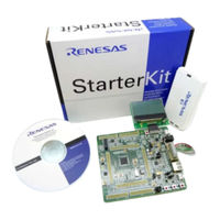
32-Bit MCU; Renesas Starter Kit
Brand:
Renesas
| Category:
Computer Hardware
| Size: 0 MB
Table of Contents
Table of Contents
9
1 Overview
11
Purpose
11
Features
11
Board Specification
12
2 Power Supply
13
Requirements
13
Power-Up Behaviour
13
3 Board Layout
14
Component Layout
14
Board Dimensions
15
Component Placement
16
4 Connectivity
18
Internal RSK Connections
18
Debugger Connections
19
5 User Circuitry
20
Reset Circuit
20
Clock Circuit
20
Switches
20
Leds
21
Potentiometer
21
Pmod
22
USB Serial Port
23
Local-Interconnect Network (LIN)
23
C Bus (Inter-IC Bus)
24
Touch Interface
24
6 Configuration
25
Modifying the RSK
25
MCU Operating Modes
25
Power Supply Configuration
26
Clock Configuration
26
Analog Power & ADC & DAC Configuration
27
E1 / E2 Lite Debugger Configuration
27
General I/O & LED Configuration
28
I 2 C & EEPROM Configuration
28
IRQ & Switch Configuration
29
LIN Configuration
29
MTU & POE Configuration
30
PMOD1 Interface Configuration
31
PMOD2 Interface Configuration
31
Serial & USB to Serial Configuration
32
Touch Interface Configuration
33
7 Headers
34
Application Headers
34
Microcontroller Pin Headers
38
8 Code Development
40
Overview
40
Compiler Restrictions
40
Mode Support
40
Debugging Support
40
Advertisement
Renesas RX100 Series User Manual (43 pages)
Starter Kit For CubeSuite+. RX111 Group
Brand:
Renesas
| Category:
Computer Hardware
| Size: 1 MB
Table of Contents
Table of Contents
7
Overview
8
Purpose
8
Features
8
Power Supply
9
Requirements
9
Power-Up Behaviour
9
Board Layout
10
Component Layout
10
Board Dimensions
11
Component Placement
12
Connectivity
13
Internal RSK Connections
13
Debugger Connections
14
User Circuitry
15
Reset Circuit
15
Clock Circuit
15
Switches
15
Leds
16
Potentiometer
16
Pmod™ Debug LCD Module
16
USB Serial Port
17
Local Interconnect Network (LIN)
18
Universal Serial Bus (USB)
18
I 2 C Bus (Inter-IC Bus)
18
Configuration
19
Modifying the RSK
19
MCU Operating Modes
19
Power Supply Configuration
20
Clock Configuration
20
ADC & DAC Configuration
21
E1 Debugger Configuration
22
I2C EEPROM Configuration
22
I/O Port Configuration
23
IRQ & Switch Configuration
24
LIN Configuration
24
MTU & POE Configuration
25
PMOD1 Interface Configuration
27
PMOD2 Interface Configuration
28
SCI & RS232 Serial Port Configuration
29
USB Configuration
30
Headers
31
Application Headers
31
Microcontroller Pin Headers
35
Code Development
37
Overview
37
Compiler Restrictions
37
Mode Support
37
Debugging Support
37
Address Space
38
Additional Information
39
Renesas RX100 Series User Manual (43 pages)
32-Bit MCU Starter Kit
Brand:
Renesas
| Category:
Microcontrollers
| Size: 0 MB
Table of Contents
Table of Contents
7
Overview
9
Purpose
9
Features
9
Board Specification
10
Power Supply
11
Requirements
11
Power-Up Behaviour
11
Board Layout
12
Component Layout
12
Board Dimensions
13
Component Placement
14
Connectivity
16
Internal Board Connections
16
Debugger Connections
17
User Circuitry
18
Reset Circuit
18
Clock Circuit
18
Switches
18
Leds
19
Potentiometer
19
Pmod
20
USB Serial Port
22
Controller Area Network (CAN)
22
Local Interconnect Network (LIN)
23
I 2 C Bus (Inter-IC Bus)
23
Touch Interface
23
Configuration
24
Modifying the RSK
24
MCU Operating Modes
24
E2 Lite Debugger Configuration
24
Power Supply Configuration
25
Clock Configuration
25
Analog Power, ADC and DAC Configuration
26
CAN Configuration
26
General IO & LED Configuration
27
I2C & EEPROM Configuration
27
IRQ & Switch Configuration
28
MTU & POE & Timer Configuration
29
PMOD1 Configuration
30
PMOD2 Configuration
30
Serial & USB to Serial Configuration
31
LIN Configuration
31
Touch Interface Configuration
32
Headers
33
Application Headers
33
Microcontroller Pin Headers
37
Code Development
39
Renesas RX100 Series User Manual (38 pages)
Starter Kit Code Generator
Brand:
Renesas
| Category:
Portable Generator
| Size: 0 MB
Table of Contents
How to Use this Manual
4
List of Abbreviations and Acronyms
5
Table of Contents
6
Overview
7
Purpose
7
Features
7
Introduction
8
Project Creation with CS
9
Introduction
9
Creating the Project
9
Code Generation Using the CS+ Plug in
10
Introduction
10
Enabling Code Generator
10
Code Generator Tour
11
Code Generation
12
Clock Generator
12
I/O Ports
14
Serial Communications Interface
15
12-Bit A/D Converter
16
Generating the Code
18
Project Settings
19
Adding Project Folders
22
User Code Integration
23
Support File Copying
23
LCD File Copying
23
Including Files in the CS+ Project
24
Adding Code to Generated Files
24
R_Cg_Userdefine.h Code Insertion
24
R_Cg_S12Ad.C Code Insertion
25
R_Cg_S12Ad.h Code Insertion
25
R_Cg_S12Ad_User.C Code Insertion
26
R_Cg_Sci_User.C Code Insertion
26
R_Cg_Sci.h Code Insertion
27
R_Cg_Main.C Code Insertion
28
Project Build and Debugger Configuration
32
Running the Tutorial
33
Additional Information
34
Revision History
35
Renesas RX100 Series User Manual (24 pages)
Target Board, 32-Bit MCU
Brand:
Renesas
| Category:
Microcontrollers
| Size: 0 MB
Table of Contents
Table of Contents
6
1 Overview
7
Contents
7
Purpose
7
Features
7
Preparation
7
Board Specification Table
8
2 Board Layout
9
3 Parts Layout
10
4 Operating Environment
11
5 User Circuit
12
Evaluation MCU
12
USB Connector
12
Act Led
12
Power LED
12
User LED
12
Pmod™ Connector
13
External Power Supply Header
14
Current Consumption Measurement Header
15
MCU Header
15
RESET Switch
15
User Switch
15
Cut Pattern
15
Emulator Reset Header
16
Power Supply Selection Header
16
6 Configuration
17
Modifying the Target Board for RX130
17
Analog Power Supply
17
On-Chip Oscillator
17
7 Handling Precautions
18
Board Thickness
18
Additional Load
18
Substrate Remodelling
18
Communication with RFP
18
8 Code Development
19
9 Additional Information
20
Advertisement
Related Products
Renesas RX700 Series
Renesas RX72N
Renesas RX220 Series
Renesas RX62T
Renesas RX72M Renesas Starter Kit
Renesas RX140
Renesas RX66N RX600 Series
Renesas RX660 Series
Renesas RX24T RX200 Series
Renesas RX24T R5F524TAADFN 10
Renesas Categories
Computer Hardware
Motherboard
Microcontrollers
Adapter
Switch
More Renesas Manuals
Login
Sign In
OR
Sign in with Facebook
Sign in with Google
Upload manual
Upload from disk
Upload from URL