Sign In
Upload
Manuals
Brands
Renesas Manuals
Computer Hardware
H8S/2368 Series
Renesas H8S/2368 Series Manuals
Manuals and User Guides for Renesas H8S/2368 Series. We have
1
Renesas H8S/2368 Series manual available for free PDF download: Hardware Manual
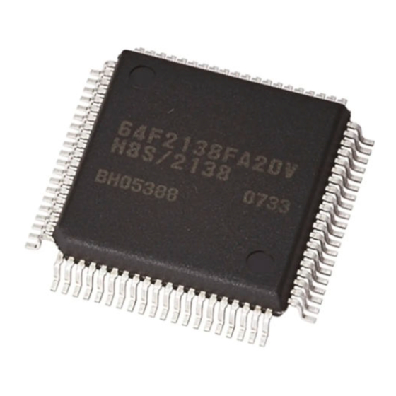
Renesas H8S/2368 Series Hardware Manual (875 pages)
16-Bit Single-Chip Microcomputer
Brand:
Renesas
| Category:
Computer Hardware
| Size: 5.48 MB
Table of Contents
General Precautions on Handling of Product
5
Preface
7
List of Registers
8
Register Bits
16
Table of Contents
21
Section 1 Overview
53
Features
53
Figure 1.1 Internal Block Diagram of H8S/2367, H8S/2365, and H8S/2363
55
Block Diagram
55
Figure
55
Figure 1.2 Internal Block Diagram of H8S/2366
56
Pin Description
57
Pin Arrangement
57
Figure 1.3 Pin Arrangement of H8S/2367, H8S/2365, and H8S/2363
57
Figure 1.4 Pin Arrangement of H8S/2366
58
Figure 1.5 Pin Arrangement of H8S/2367, H8S/2365, and H8S/2363
59
Figure 1.6 Pin Arrangement of H8S/2366
60
Pin Arrangement in each Operating Mode
61
Table 1.1 Pin Arrangement in each Operating Mode
61
Manual
62
Pin Functions
66
Table 1.2 Pin Functions
66
Section 2 CPU
73
Features
73
Differences between H8S/2600 CPU and H8S/2000 CPU
74
Differences from H8/300 CPU
75
Differences from H8/300H CPU
75
CPU Operating Modes
76
Normal Mode
76
Advanced Mode
77
Figure 2.1 Exception Vector Table (Normal Mode)
77
Figure 2.2 Stack Structure in Normal Mode
77
Figure 2.3 Exception Vector Table (Advanced Mode)
78
Figure 2.4 Stack Structure in Advanced Mode
79
Figure 2.5 Memory Map
80
Address Space
80
Figure 2.6 CPU Internal Registers
81
Figure 2.7 Usage of General Registers
82
General Registers
82
Extended Control Register (EXR)
83
Program Counter (PC)
83
Stack
83
Condition-Code Register (CCR)
84
Initial Register Values
86
Register Configuration
81
Data Formats
86
Figure 2.9 General Register Data Formats (1)
86
General Register Data Formats
86
Figure 2.9 General Register Data Formats (2)
87
Figure 2.10 Memory Data Formats
88
Memory Data Formats
88
Table 2.1
89
Table 2.2 Operation Notation
90
Table of Instructions Classified by Function
90
Table 2.3 Data Transfer Instructions
91
Table 2.4 Arithmetic Operations Instructions
92
Table 2.5 Logic Operations Instructions
94
Table 2.6 Shift Instructions
94
Table 2.7 Bit Manipulation Instructions
95
Table 2.8 Branch Instructions
97
Table 2.9 System Control Instructions
98
Basic Instruction Formats
99
Table 2.10 Block Data Transfer Instructions
99
Instruction Set
89
Table 2.11 Addressing Modes
100
Absolute Address-@Aa:8, @Aa:16, @Aa:24, or @Aa:32
101
Register Direct-Rn
101
Register Indirect with Displacement-@(D:16, Ern) or @(D:32, Ern)
101
Register Indirect with Post-Increment or Pre-Decrement-@Ern+ or @-Ern
101
Register Indirect-@Ern
101
Immediate-#XX:8, #XX:16, or #XX:32
102
Memory Indirect-@@Aa:8
102
Program-Counter Relative-@(D:8, PC) or @(D:16, PC)
102
Table 2.12 Absolute Address Access Ranges
102
Effective Address Calculation
103
Figure 2.12 Branch Address Specification in Memory Indirect Addressing Mode
103
Table 2.13 Effective Address Calculation
104
Figure 2.11 Instruction Formats (Examples)
100
Addressing Modes and Effective Address Calculation
100
Processing States
106
Usage Note
107
Note on Bit Manipulation Instructions
107
Figure 2.13 State Transitions
107
Section 3 MCU Operating Modes
109
Operating Mode Selection
109
Register Descriptions
110
Mode Control Register (MDCR)
110
System Control Register (SYSCR)
110
Operating Mode Descriptions
112
Mode 1
112
Mode 2
112
Mode 3
112
Mode 4
112
Mode 7
113
Pin Functions
113
Table 3.2 Pin Functions in each Operating Mode
113
Memory Map in each Operating Mode
114
Figure 3.1 H8S/2367 Memory Map (1)
114
Figure 3.2 H8S/2367 Memory Map (2)
115
Figure 3.3 H8S/2366 Memory Map (1)
116
Figure 3.4 H8S/2366 Memory Map (2)
117
Figure 3.5 H8S/2365 Memory Map (1)
118
Figure 3.6 H8S/2365 Memory Map (2)
119
Figure 3.7 H8S/2363 Memory Map
120
Section 4 Exception Handling
121
Table 4.1 Exception Types and Priority
121
Exception Handling Types and Priority
121
Exception Sources and Exception Vector Table
121
Table 4.2 Exception Handling Vector Table
122
Reset
123
Reset Exception Handling
123
Figure 4.1 Reset Sequence (Advanced Mode with On-Chip ROM Enabled)
124
Interrupts after Reset
125
On-Chip Peripheral Functions after Reset Release
125
Figure 4.2 Reset Sequence (Advanced Mode with On-Chip ROM Disabled)
125
Table 4.3 Status of CCR and EXR after Trace Exception Handling
126
Traces
126
Interrupts
126
Table 4.4 Status of CCR and EXR after Trap Instruction Exception Handling
127
Trap Instruction
127
Stack Status after Exception Handling
128
Figure 4.3 Stack Status after Exception Handling
128
Usage Notes
129
Figure 4.4 Operation When SP Value Is Odd
129
Section 5 Interrupt Controller
131
Features
131
Figure 5.1 Block Diagram of Interrupt Controller
132
Table 5.1 Pin Configuration
133
Interrupt Control Register (INTCR)
134
Interrupt Priority Registers a to K (IPRA to IPRK)
134
IRQ Enable Register (IER)
136
IRQ Sense Control Register L (ISCRL)
137
IRQ Status Register (ISR)
140
IRQ Pin Select Register (ITSR)
141
Software Standby Release IRQ Enable Register (SSIER)
142
Input/Output Pins
133
Register Descriptions
133
Interrupt Sources
142
External Interrupts
142
Internal Interrupts
143
Figure 5.2 Block Diagram of Interrupts IRQ15 to IRQ0
143
Interrupt Exception Handling Vector Table
144
Table 5.2 Interrupt Sources, Vector Addresses, and Interrupt Priorities
145
Interrupt Control Modes and Interrupt Operation
149
Interrupt Control Mode 0
149
Table 5.3 Interrupt Control Modes
149
Figure 5.3 Flowchart of Procedure up to Interrupt Acceptance
150
Interrupt Control Mode 2
151
Interrupt Exception Handling Sequence
152
Figure 5.4 Flowchart of Procedure up to Interrupt Acceptance in Interrupt Control Mode 2
152
Figure 5.5 Interrupt Exception Handling
153
Interrupt Response Times
154
Table 5.4 Interrupt Response Times
154
Table 5.5 Number of States in Interrupt Handling Routine Execution Statuses
154
DTC and DMAC* Activation by Interrupt
155
Usage Notes
155
Contention between Interrupt Generation and Disabling
155
Instructions that Disable Interrupts
156
Times When Interrupts Are Disabled
156
Interrupts During Execution of EEPMOV Instruction
156
Figure 5.6 Contention between Interrupt Generation and Disabling
156
Change of IRQ Pin Select Register (ITSR) Setting
157
Note on IRQ Status Register (ISR)
157
Section 6 Bus Controller (BSC)
159
Features
159
Figure 6.1 Block Diagram of Bus Controller
160
Input/Output Pins
161
Table 6.1 Pin Configuration
161
Register Descriptions
162
Bus Width Control Register (ABWCR)
163
Access State Control Register (ASTCR)
163
Wait Control Registers AH, AL, BH, and BL (WTCRAH, WTCRAL, WTCRBH, and WTCRBL)
164
Read Strobe Timing Control Register (RDNCR)
169
Figure 6.2 Read Strobe Negation Timing (Example of 3-State Access Space)
169
CS Assertion Period Control Registers H, L (CSACRH, CSACRL)
170
Figure 6.3 CS and Address Assertion Period Extension (Example of 3-State Access Space and Rdnn = 0)
171
Area 0 Burst ROM Interface Control Register (BROMCRH) Area 1 Burst ROM Interface Control Register (BROMCRL)
172
Bus Control Register (BCR)
173
DRAM Control Register (DRAMCR)
175
Figure 6.4 RAS Signal Assertion Timing
179
DRAM Access Control Register (DRACCR)
180
Refresh Control Register (REFCR)
181
Refresh Timer Counter (RTCNT)
184
Refresh Time Constant Register (RTCOR)
184
Operation
184
Area Division
184
Figure 6.5 Area Divisions
185
Bus Specifications
186
Table 6.2 Bus Specifications for each Area (Basic Bus Interface)
187
Memory Interfaces
188
Chip Select Signals
189
Figure 6.6 Csn Signal Output Timing (N = 0 to 7)
189
Basic Bus Interface
190
Data Size and Data Alignment
190
Figure 6.7 Access Sizes and Data Alignment Control (8-Bit Access Space)
190
Valid Strobes
191
Figure 6.8 Access Sizes and Data Alignment Control (16-Bit Access Space)
191
Table 6.3 Data Buses Used and Valid Strobes
191
Basic Timing
192
Figure 6.9 Bus Timing for 8-Bit, 2-State Access Space
192
Figure 6.10 Bus Timing for 8-Bit, 3-State Access Space
193
Figure 6.11 Bus Timing for 16-Bit, 2-State Access Space (Even Address Byte Access)
194
Figure 6.12 Bus Timing for 16-Bit, 2-State Access Space (Odd Address Byte Access)
195
Figure 6.13 Bus Timing for 16-Bit, 2-State Access Space (Word Access)
196
Figure 6.14 Bus Timing for 16-Bit, 3-State Access Space (Even Address Byte Access)
197
Figure 6.15 Bus Timing for 16-Bit, 3-State Access Space (Odd Address Byte Access)
198
Figure 6.16 Bus Timing for 16-Bit, 3-State Access Space (Word Access)
199
Wait Control
200
Read Strobe (RD) Timing
201
Figure 6.17 Example of Wait State Insertion Timing
201
Extension of Chip Select (CS) Assertion Period
202
Figure 6.18 Example of Read Strobe Timing
202
Figure 6.19 Example of Timing When Chip Select Assertion Period Is Extended
203
DRAM Interface
204
Setting DRAM Space
204
Address Multiplexing
204
Table 6.4 Relation between Settings of Bits RMTS2 to RMTS0 and DRAM Space
204
Data Bus
205
Table 6.5 Relation between Settings of Bits MXC2 to MXC0 and Address Multiplexing
205
Pins Used for DRAM Interface
206
Table 6.6 DRAM Interface Pins
206
Basic Timing
207
Figure 6.20 DRAM Basic Access Timing (RAST = 0, CAST = 0)
207
Column Address Output Cycle Control
208
Row Address Output State Control
208
Figure 6.21 Example of Access Timing with 3-State Column Address Output Cycle (RAST = 0)
208
Figure 6.22 Example of Access Timing When RAS Signal Goes Low from Beginning of T State (CAST = 0)
209
Figure 6.23 Example of Timing with One Row Address Output Maintenance State (RAST = 0, CAST = 0)
210
Precharge State Control
211
Figure 6.24 Example of Timing with Two-State Precharge Cycle (RAST = 0, CAST = 0)
211
Wait Control
212
Figure 6.25 Example of Wait State Insertion Timing (2-State Column Address Output)
213
Figure 6.26 Example of Wait State Insertion Timing (3-State Column Address Output)
214
Byte Access Control
215
Figure 6.27 2-CAS Control Timing (Upper Byte Write Access: RAST = 0, CAST = 0)
215
Burst Operation
216
Figure 6.28 Example of 2-CAS DRAM Connection
216
Figure 6.29 Operation Timing in Fast Page Mode (RAST = 0, CAST = 0)
217
Figure 6.30 Operation Timing in Fast Page Mode (RAST = 0, CAST = 1)
218
Figure 6.31 Example of Operation Timing in RAS down Mode (RAST = 0, CAST = 0)
219
Refresh Control
220
Figure 6.32 Example of Operation Timing in RAS up Mode (RAST = 0, CAST = 0)
220
Figure 6.33 RTCNT Operation
221
Figure 6.34 Compare Match Timing
221
Figure 6.35 CBR Refresh Timing
222
Figure 6.36 CBR Refresh Timing (RCW1 = 0, RCW0 = 1, RLW1 = 0, RLW0 = 0)
222
Figure 6.37 Example of CBR Refresh Timing (CBRM = 1)
223
Figure 6.38 Self-Refresh Timing
224
DMAC Single Address Transfer Mode and DRAM Interface
225
Figure 6.39 Example of Timing When Precharge Time after Self-Refreshing Is Extended by 2 States
225
Figure 6.40 Example of DACK Output Timing When DDS = 1 (RAST = 0, CAST = 0)
226
Figure 6.41 Example of DACK Output Timing When DDS = 0 (RAST = 0, CAST = 1)
227
Burst ROM Interface
228
Basic Timing
228
Figure 6.42 Example of Burst ROM Access Timing (Astn = 1, 2-State Burst Cycle)
229
Wait Control
230
Write Access
230
Figure 6.43 Example of Burst ROM Access Timing (Astn = 0, 1-State Burst Cycle)
230
Idle Cycle
231
Operation
231
Figure 6.44 Example of Idle Cycle Operation (Consecutive Reads in Different Areas)
231
Figure 6.45 Example of Idle Cycle Operation (Write after Read)
232
Figure 6.46 Example of Idle Cycle Operation (Read after Write)
233
Figure 6.47 Relationship between Chip Select (CS) and Read (RD)
234
Figure 6.48 Example of DRAM Full Access after External Read (CAST = 0)
234
Figure 6.49 Example of Idle Cycle Operation in RAS down Mode (Consecutive Reads in Different Areas) (IDLC = 0, RAST = 0, CAST = 0)
235
Figure 6.50 Example of Idle Cycle Operation in RAS down Mode (Write after Read) (IDLC = 0, RAST = 0, CAST = 0)
235
Figure 6.51 Example of Idle Cycle Operation after DRAM Access (Consecutive Reads in Different Areas) (IDLC = 0, RAST = 0, CAST = 0)
236
Figure 6.52 Example of Idle Cycle Operation after DRAM Access (Write after Read) (IDLC = 0, RAST = 0, CAST = 0)
237
Figure 6.53 Example of Idle Cycle Operation after DRAM Write Access (IDLC = 0, ICIS1 = 0, RAST = 0, CAST = 0)
238
Table 6.7 Idle Cycles in Mixed Accesses to Normal Space and DRAM
239
Figure 6.54 Example of Timing for Idle Cycle Insertion in Case of Consecutive Read
240
Pin States in Idle Cycle
241
Write Data Buffer Function
241
Table 6.8 Pin States in Idle Cycle
241
Bus Release
242
Operation
242
Figure 6.55 Example of Timing When Write Data Buffer Function Is Used
242
Pin States in External Bus Released State
244
Table 6.9 Pin States in Bus Released State
244
Transition Timing
245
Figure 6.56 Bus Released State Transition Timing
245
Bus Arbitration
246
Operation
246
Bus Transfer Timing
247
Bus Controller Operation in Reset
248
Usage Notes
248
External Bus Release Function and All-Module-Clocks-Stopped Mode
248
External Bus Release Function and Software Standby
248
External Bus Release Function and CBR Refreshing
248
BREQO Output Timing
249
Section 7 DMA Controller (DMAC)
251
Features
251
Figure 7.1 Block Diagram of DMAC
252
Register Descriptions
253
Table 7.1 Pin Configuration
253
Memory Address Registers (MARA and MARB)
254
Table 7.2 Short Address Mode and Full Address Mode (Channel 0)
254
Execute Transfer Count Registers (ETCRA and ETCRB)
255
I/O Address Registers (IOARA and IOARB)
255
DMA Control Registers (DMACRA and DMACRB)
256
DMA Band Control Registers H and L (DMABCRH and DMABCRL)
263
DMA Write Enable Register (DMAWER)
275
Figure 7.2 Areas for Register Re-Setting by DTC (Channel 0A)
276
DMA Terminal Control Register (DMATCR)
277
Input/Output Pins
253
Activation Sources
278
Activation by Internal Interrupt Request
278
Table 7.3 DMAC Activation Sources
278
Activation by External Request
279
Activation by Auto-Request
279
Operation
280
Transfer Modes
280
Table 7.4 DMAC Transfer Modes
280
Sequential Mode
282
Table 7.5 Register Functions in Sequential Mode
282
Figure 7.3 Operation in Sequential Mode
283
Idle Mode
284
Figure 7.4 Example of Sequential Mode Setting Procedure
284
Figure 7.5 Operation in Idle Mode
285
Table 7.6 Register Functions in Idle Mode
285
Repeat Mode
286
Figure 7.6 Example of Idle Mode Setting Procedure
286
Table 7.7 Register Functions in Repeat Mode
287
Figure 7.7 Operation in Repeat Mode
288
Single Address Mode
289
Figure 7.8 Example of Repeat Mode Setting Procedure
289
Table 7.8 Register Functions in Single Address Mode
290
Figure 7.9 Operation in Single Address Mode (When Sequential Mode Is Specified)
291
Normal Mode
292
Figure 7.10 Example of Single Address Mode Setting Procedure (When Sequential Mode Is Specified)
292
Table 7.9 Register Functions in Normal Mode
293
Figure 7.11 Operation in Normal Mode
294
Block Transfer Mode
295
Figure 7.12 Example of Normal Mode Setting Procedure
295
Table 7.10 Register Functions in Block Transfer Mode
296
Figure 7.13 Operation in Block Transfer Mode (BLKDIR = 0)
297
Figure 7.14 Operation in Block Transfer Mode (BLKDIR = 1)
298
Figure 7.15 Operation Flow in Block Transfer Mode
299
Figure 7.16 Example of Block Transfer Mode Setting Procedure
300
Basic Bus Cycles
301
DMA Transfer (Dual Address Mode) Bus Cycles
301
Figure 7.17 Example of DMA Transfer Bus Timing
301
Figure 7.18 Example of Short Address Mode Transfer
302
Figure 7.19 Example of Full Address Mode Transfer (Cycle Steal)
303
Figure 7.20 Example of Full Address Mode Transfer (Burst Mode)
304
Figure 7.21 Example of Full Address Mode Transfer (Block Transfer Mode)
305
Figure 7.22 Example of DREQ Pin Falling Edge Activated Normal Mode Transfer
306
Figure 7.23 Example of DREQ Pin Falling Edge Activated Block Transfer Mode Transfer
307
Figure 7.24 Example of DREQ Pin Low Level Activated Normal Mode Transfer
308
DMA Transfer (Single Address Mode) Bus Cycles
309
Figure 7.25 Example of DREQ Pin Low Level Activated Block Transfer Mode Transfer
309
Figure 7.26 Example of Single Address Mode Transfer (Byte Read)
310
Figure 7.27 Example of Single Address Mode (Word Read) Transfer
310
Figure 7.28 Example of Single Address Mode Transfer (Byte Write)
311
Figure 7.29 Example of Single Address Mode Transfer (Word Write)
312
Figure 7.30 Example of DREQ Pin Falling Edge Activated Single Address Mode Transfer
313
Figure 7.31 Example of DREQ Pin Low Level Activated Single Address Mode Transfer
314
Write Data Buffer Function
315
Figure 7.32 Example of Dual Address Transfer Using Write Data Buffer Function
315
Multi-Channel Operation
316
Figure 7.33 Example of Single Address Transfer Using Write Data Buffer Function
316
Table 7.11 DMAC Channel Priority Order
316
Relation between DMAC and External Bus Requests and Refresh Cycles
317
Figure 7.34 Example of Multi-Channel Transfer
317
DMAC and NMI Interrupts
318
Forced Termination of DMAC Operation
318
Figure 7.35 Example of Procedure for Continuing Transfer on Channel Interrupted
318
Clearing Full Address Mode
319
Figure 7.36 Example of Procedure for Forcibly Terminating DMAC Operation
319
Table 7.12 Interrupt Sources and Priority Order
320
Figure 7.37 Example of Procedure for Clearing Full Address Mode
320
Interrupt Sources
320
Usage Notes
321
DMAC Register Access During Operation
321
Figure 7.38 Block Diagram of Transfer End/Transfer Break Interrupt
321
Figure 7.39 DMAC Register Update Timing
322
Figure 7.40 Contention between DMAC Register Update and CPU Read
322
Module Stop
323
Write Data Buffer Function
323
TEND Output
323
Activation by Falling Edge on DREQ Pin
324
Figure 7.41 Example in Which Low Level Is Not Output at TEND Pin
324
Activation Source Acceptance
325
Internal Interrupt after End of Transfer
325
Channel Re-Setting
325
Section 8 Data Transfer Controller (DTC)
327
Features
327
Figure 8.1 Block Diagram of DTC
328
DTC Mode Register a (MRA)
329
DTC Destination Address Register (DAR)
330
DTC Mode Register B (MRB)
330
DTC Source Address Register (SAR)
330
DTC Transfer Count Register a (CRA)
330
DTC Enable Registers a to G (DTCERA to DTCERG)
331
DTC Transfer Count Register B (CRB)
331
DTC Vector Register (DTVECR)
331
Register Descriptions
328
Activation Sources
332
Location of Register Information and DTC Vector Table
333
Table 8.1 Relationship between Activation Sources and DTCER Clearing
333
Figure 8.2 Block Diagram of DTC Activation Source Control
333
Figure 8.3 Correspondence between DTC Vector Address and Register Information
334
Figure 8.4 Correspondence between DTC Vector Address and Register Information
334
Table 8.2 Interrupt Sources, DTC Vector Addresses, and Corresponding Dtces
335
Operation
336
Figure 8.5 Flowchart of DTC Operation
337
Normal Mode
338
Table 8.3 Chain Transfer Conditions
338
Table 8.4 Register Function in Normal Mode
338
Figure 8.6 Memory Mapping in Normal Mode
339
Repeat Mode
339
Table 8.5 Register Function in Repeat Mode
339
Block Transfer Mode
340
Figure 8.7 Memory Mapping in Repeat Mode
340
Table 8.6 Register Function in Block Transfer Mode
340
Chain Transfer
341
Figure 8.8 Memory Mapping in Block Transfer Mode
341
Figure 8.9 Operation of Chain Transfer
342
Interrupts
342
Figure 8.10 DTC Operation Timing (Example in Normal Mode or Repeat Mode)
343
Figure 8.11 DTC Operation Timing (Example of Block Transfer Mode, with Block Size of 2)
343
Figure 8.12 DTC Operation Timing (Example of Chain Transfer)
343
Operation Timing
343
Number of DTC Execution States
344
Table 8.7 DTC Execution Status
344
Table 8.8 Number of States Required for each Execution Status
344
Procedures for Using DTC
345
Activation by Interrupt
345
Activation by Software
345
Examples of Use of the DTC
345
Normal Mode
345
Chain Transfer
346
Chain Transfer When Counter = 0
347
Software Activation
348
Figure 8.13 Chain Transfer When Counter = 0
348
Usage Notes
349
Module Stop Mode Setting
349
On-Chip RAM
349
DTCE Bit Setting
349
DMAC Transfer End Interrupt
349
Chain Transfer
349
Section 9 I/O Ports
351
Table 9.1 Port Functions
352
Port 1
355
Port 1 Data Direction Register (P1DDR)
355
Port 1 Data Register (P1DR)
356
Port 1 Register (PORT1)
356
Pin Functions
357
Port 2
365
Port 2 Data Direction Register (P2DDR)
365
Port 2 Data Register (P2DR)
365
Port 2 Register (PORT2)
366
Pin Functions
367
Port 3
375
Port 3 Data Direction Register (P3DDR)
375
Port 3 Data Register (P3DR)
376
Port 3 Register (PORT3)
376
Port 3 Open Drain Control Register (P3ODR)
377
Port Function Control Register 2 (PFCR2)
378
Pin Functions
379
Port 4
382
Port 4 Register (PORT4)
382
Pin Functions
383
Port 5
385
Port 5 Data Direction Register (P5DDR)
385
Port 5 Data Register (P5DR)
385
Port 5 Register (PORT5)
386
Pin Functions
386
Port 8
388
Port 8 Data Direction Register (P8DDR)
388
Port 8 Data Register (P8DR)
389
Port 8 Register (PORT8)
389
Pin Functions
390
Port 9
391
Port 9 Register (PORT9)
391
Pin Functions
391
Port a
392
Port a Data Direction Register (PADDR)
393
Port a Data Register (PADR)
394
Port a Register (PORTA)
394
Port a MOS Pull-Up Control Register (PAPCR)
395
Port a Open Drain Control Register (PAODR)
395
Port Function Control Register 0 (PFCR0)
396
Port Function Control Register 1 (PFCR1)
396
Pin Functions
397
Port a MOS Input Pull-Up States
399
Table 9.2 MOS Input Pull-Up States (Port A)
399
Port B
400
Port B Data Direction Register (PBDDR)
400
Port B Data Register (PBDR)
401
Port B Register (PORTB)
401
Port B MOS Pull-Up Control Register (PBPCR)
402
Pin Functions
402
Port B MOS Input Pull-Up States
403
Table 9.3 MOS Input Pull-Up States (Port B)
403
Port C
404
Port C Data Direction Register (PCDDR)
404
Port C Data Register (PCDR)
405
Port C Register (PORTC)
405
Port C MOS Pull-Up Control Register (PCPCR)
406
Pin Functions
406
Port C MOS Input Pull-Up States
407
Table 9.4 MOS Input Pull-Up States (Port C)
407
Port D
408
Port D Data Direction Register (PDDDR)
408
Port D Data Register (PDDR)
408
Port D Register (PORTD)
409
Port D Pull-Up Control Register (PDPCR)
409
Pin Functions
410
Port D MOS Input Pull-Up States
410
Table 9.5 MOS Input Pull-Up States (Port D)
410
Port E
411
Port E Data Direction Register (PEDDR)
411
Port E Data Register (PEDR)
412
Port E Register (PORTE)
412
Port E Pull-Up Control Register (PEPCR)
413
Pin Functions
413
Port E MOS Input Pull-Up States
414
Port F
414
Table 9.6 MOS Input Pull-Up States (Port E)
414
Port F Data Direction Register (PFDDR)
415
Port F Data Register (PFDR)
416
Port F Register (PORTF)
416
Pin Functions
417
Port G
420
Port G Data Direction Register
420
Port G Data Register
422
Port G Register (PORTG)
422
Pin Functions
423
Section 10 16-Bit Timer Pulse Unit (TPU)
425
Features
425
Table 10.1 TPU Functions
426
Figure 10.1 Block Diagram of TPU
428
Table 10.2 Pin Configuration
429
Input/Output Pins
429
Register Descriptions
430
Timer Control Register (TCR)
432
Table 10.3 CCLR2 to CCLR0 (Channels 0 and 3)
433
Table 10.4 CCLR2 to CCLR0 (Channels 1, 2, 4, and 5)
433
Table 10.5 TPSC2 to TPSC0 (Channel 0)
434
Table 10.6 TPSC2 to TPSC0 (Channel 1)
434
Table 10.7 TPSC2 to TPSC0 (Channel 2)
435
Table 10.8 TPSC2 to TPSC0 (Channel 3)
435
Table 10.9 TPSC2 to TPSC0 (Channel 4)
436
Table 10.10 TPSC2 to TPSC0 (Channel 5)
436
Timer Mode Register (TMDR)
437
Timer I/O Control Register (TIOR)
438
Table 10.11 MD3 to MD0
438
Table 10.12 TIORH_0
440
Table 10.13 TIORL_0
441
Table 10.14 TIOR_1
442
Table 10.15 TIOR_2
443
Table 10.16 TIORH_3
444
Table 10.17 TIORL_3
445
Table 10.18 TIOR_4
446
Table 10.19 TIOR_5
447
Table 10.20 TIORH_0
448
Table 10.21 TIORL_0
449
Table 10.22 TIOR_1
450
Table 10.23 TIOR_2
451
Table 10.24 TIORH_3
452
Table 10.25 TIORL_3
453
Table 10.26 TIOR_4
454
Table 10.27 TIOR_5
455
Timer Interrupt Enable Register (TIER)
456
Timer Status Register (TSR)
458
Timer Counter (TCNT)
460
Timer General Register (TGR)
461
Timer Start Register (TSTR)
461
Timer Synchronous Register (TSYR)
462
Operation
463
Basic Functions
463
Figure 10.2 Example of Counter Operation Setting Procedure
463
Figure 10.3 Free-Running Counter Operation
464
Figure 10.4 Periodic Counter Operation
465
Figure 10.5 Example of Setting Procedure for Waveform Output by Compare Match
465
Figure 10.6 Example of 0 Output/1 Output Operation
466
Figure 10.7 Example of Toggle Output Operation
466
Figure 10.8 Example of Setting Procedure for Input Capture Operation
467
Synchronous Operation
468
Figure 10.9 Example of Input Capture Operation
468
Figure 10.10 Example of Synchronous Operation Setting Procedure
469
Buffer Operation
470
Figure 10.11 Example of Synchronous Operation
470
Table 10.28 Register Combinations in Buffer Operation
470
Figure 10.12 Compare Match Buffer Operation
471
Figure 10.13 Input Capture Buffer Operation
471
Figure 10.14 Example of Buffer Operation Setting Procedure
472
Figure 10.15 Example of Buffer Operation (1)
473
Cascaded Operation
474
Figure 10.16 Example of Buffer Operation (2)
474
Table 10.29 Cascaded Combinations
474
Figure 10.17 Cascaded Operation Setting Procedure
475
Figure 10.18 Example of Cascaded Operation (1)
475
PWM Modes
476
Figure 10.19 Example of Cascaded Operation (2)
476
Table 10.30 PWM Output Registers and Output Pins
477
Figure 10.20 Example of PWM Mode Setting Procedure
478
Figure 10.21 Example of PWM Mode Operation (1)
479
Figure 10.22 Example of PWM Mode Operation (2)
479
Figure 10.23 Example of PWM Mode Operation (3)
480
Phase Counting Mode
481
Figure 10.24 Example of Phase Counting Mode Setting Procedure
481
Table 10.31 Clock Input Pins in Phase Counting Mode
481
Figure 10.25 Example of Phase Counting Mode 1 Operation
482
Table 10.32 Up/Down-Count Conditions in Phase Counting Mode 1
482
Figure 10.26 Example of Phase Counting Mode 2 Operation
483
Table 10.33 Up/Down-Count Conditions in Phase Counting Mode 2
483
Figure 10.27 Example of Phase Counting Mode 3 Operation
484
Table 10.34 Up/Down-Count Conditions in Phase Counting Mode 3
484
Figure 10.28 Example of Phase Counting Mode 4 Operation
485
Table 10.35 Up/Down-Count Conditions in Phase Counting Mode 4
485
Figure 10.29 Phase Counting Mode Application Example
486
Interrupts
487
Table 10.36 TPU Interrupts
488
DTC Activation
489
DMAC Activation
489
A/D Converter Activation
489
Operation Timing
490
Input/Output Timing
490
Figure 10.30 Count Timing in Internal Clock Operation
490
Figure 10.31 Count Timing in External Clock Operation
490
Figure 10.32 Output Compare Output Timing
491
Figure 10.33 Input Capture Input Signal Timing
491
Figure 10.34 Counter Clear Timing (Compare Match)
492
Figure 10.35 Counter Clear Timing (Input Capture)
492
Figure 10.36 Buffer Operation Timing (Compare Match)
492
Interrupt Signal Timing
493
Figure 10.37 Buffer Operation Timing (Input Capture)
493
Figure 10.38 TGI Interrupt Timing (Compare Match)
493
Figure 10.39 TGI Interrupt Timing (Input Capture)
494
Figure 10.40 TCIV Interrupt Setting Timing
494
Figure 10.41 TCIU Interrupt Setting Timing
495
Figure 10.42 Timing for Status Flag Clearing by CPU
495
Usage Notes
496
10.10.1 Module Stop Mode Setting
496
10.10.2 Input Clock Restrictions
496
Figure 10.43 Timing for Status Flag Clearing by DTC/DMAC Activation
496
10.10.3 Caution on Cycle Setting
497
10.10.4 Contention between TCNT Write and Clear Operations
497
Figure 10.44 Phase Difference, Overlap, and Pulse Width in Phase Counting Mode
497
10.10.5 Contention between TCNT Write and Increment Operations
498
Figure 10.45 Contention between TCNT Write and Clear Operations
498
Figure 10.46 Contention between TCNT Write and Increment Operations
498
10.10.6 Contention between TGR Write and Compare Match
499
10.10.7 Contention between Buffer Register Write and Compare Match
499
Figure 10.47 Contention between TGR Write and Compare Match
499
10.10.8 Contention between TGR Read and Input Capture
500
Figure 10.48 Contention between Buffer Register Write and Compare Match
500
Figure 10.49 Contention between TGR Read and Input Capture
500
10.10.9 Contention between TGR Write and Input Capture
501
10.10.10 Contention between Buffer Register Write and Input Capture
501
Figure 10.50 Contention between TGR Write and Input Capture
501
10.10.11 Contention between Overflow/Underflow and Counter Clearing
502
Figure 10.51 Contention between Buffer Register Write and Input Capture
502
Figure 10.52 Contention between Overflow and Counter Clearing
502
10.10.12 Contention between TCNT Write and Overflow/Underflow
503
10.10.13 Multiplexing of I/O Pins
503
10.10.14 Interrupts and Module Stop Mode
503
Figure 10.53 Contention between TCNT Write and Overflow
503
Section 11 Programmable Pulse Generator (PPG)
505
Features
505
Figure 11.1 Block Diagram of PPG
506
Table 11.1 Pin Configuration
507
Next Data Enable Registers H, L (NDERH, NDERL)
508
Output Data Registers H, L (PODRH, PODRL)
509
Next Data Registers H, L (NDRH, NDRL)
510
PPG Output Control Register (PCR)
512
PPG Output Mode Register (PMR)
513
Input/Output Pins
507
Register Descriptions
507
Figure 11.2 Overview Diagram of PPG
515
Figure 11.3 Timing of Transfer and Output of NDR Contents (Example)
516
Output Timing
516
Figure 11.4 Setup Procedure for Normal Pulse Output (Example)
517
Sample Setup Procedure for Normal Pulse Output
517
Example of Normal Pulse Output (Example of Five-Phase Pulse Output)
518
Figure 11.5 Normal Pulse Output Example (Five-Phase Pulse Output)
518
Figure 11.6 Non-Overlapping Pulse Output
519
Non-Overlapping Pulse Output
519
Figure 11.7 Non-Overlapping Operation and NDR Write Timing
520
Sample Setup Procedure for Non-Overlapping Pulse Output
520
Example of Non-Overlapping Pulse Output (Example of Four-Phase Complementary Non-Overlapping Output)
521
Figure 11.8 Setup Procedure for Non-Overlapping Pulse Output (Example)
521
Figure 11.9 Non-Overlapping Pulse Output Example (Four-Phase Complementary)
522
Figure 11.10 Inverted Pulse Output (Example)
523
Inverted Pulse Output
523
Pulse Output Triggered by Input Capture
524
Operation
515
Usage Notes
524
Module Stop Mode Setting
524
Operation of Pulse Output Pins
524
Figure 11.11 Pulse Output Triggered by Input Capture (Example)
524
Section 12 8-Bit Timers (TMR)
525
Features
525
Figure 12.1 Block Diagram of 8-Bit Timer Module
526
Input/Output Pins
527
Register Descriptions
527
Timer Counter (TCNT)
527
Table 12.1 Pin Configuration
527
Time Constant Register a (TCORA)
528
Time Constant Register B (TCORB)
528
Timer Control Register (TCR)
528
Timer Control/Status Register (TCSR)
530
Table 12.2 Clock Input to TCNT and Count Condition
530
Operation
533
Pulse Output
533
Operation Timing
534
TCNT Incrementation Timing
534
Figure 12.2 Example of Pulse Output
534
Figure 12.3 Count Timing for Internal Clock Input
534
Timing of CMFA and CMFB Setting When Compare-Match Occurs
535
Timing of Timer Output When Compare-Match Occurs
535
Figure 12.4 Count Timing for External Clock Input
535
Figure 12.5 Timing of CMF Setting
535
Timing of Compare Match Clear
536
Timing of TCNT External Reset
536
Figure 12.6 Timing of Timer Output
536
Figure 12.7 Timing of Compare Match Clear
536
Timing of Overflow Flag (OVF) Setting
537
Operation with Cascaded Connection
537
16-Bit Counter Mode
537
Figure 12.8 Timing of Clearance by External Reset
537
Figure 12.9 Timing of OVF Setting
537
Compare Match Count Mode
538
Interrupts
538
Interrupt Sources and DTC Activation
538
A/D Converter Activation
539
Table 12.3 8-Bit Timer Interrupt Sources
539
Usage Notes
540
Contention between TCNT Write and Clear
540
Contention between TCNT Write and Increment
540
Figure 12.10 Contention between TCNT Write and Clear
540
Contention between TCOR Write and Compare Match
541
Figure 12.11 Contention between TCNT Write and Increment
541
Contention between Compare Matches a and B
542
Figure 12.12 Contention between TCOR Write and Compare Match
542
Table 12.4 Timer Output Priorities
542
Switching of Internal Clocks and TCNT Operation
543
Table 12.5 Switching of Internal Clock and TCNT Operation
544
Mode Setting with Cascaded Connection
545
Interrupts in Module Stop Mode
545
Section 13 Watchdog Timer
547
Features
547
Input/Output Pin
548
Table 13.1 Pin Configuration
548
Figure 13.1 Block Diagram of WDT
548
Register Descriptions
549
Timer Counter (TCNT)
549
Timer Control/Status Register (TCSR)
549
Reset Control/Status Register (RSTCSR)
551
Operation
552
Watchdog Timer Mode
552
Interval Timer Mode
553
Figure 13.2 Operation in Watchdog Timer Mode
553
Interrupts
554
Usage Notes
554
Notes on Register Access
554
Figure 13.3 Operation in Interval Timer Mode
554
Table 13.2 WDT Interrupt Source
554
Contention between Timer Counter (TCNT) Write and Increment
555
Figure 13.4 Writing to TCNT, TCSR, and RSTCSR
555
Changing Value of CKS2 to CKS0
556
Switching between Watchdog Timer Mode and Interval Timer Mode
556
Internal Reset in Watchdog Timer Mode
556
Figure 13.5 Contention between TCNT Write and Increment
556
System Reset by WDTOVF Signal
557
Figure 13.6 Circuit for System Reset by WDTOVF Signal (Example)
557
Section 14 Serial Communication Interface (SCI, Irda)
559
Features
559
Figure 14.1 Block Diagram of SCI
560
Input/Output Pins
561
Table 14.1 Pin Configuration
561
Register Descriptions
562
Receive Shift Register (RSR)
563
Receive Data Register (RDR)
563
Transmit Data Register (TDR)
563
Transmit Shift Register (TSR)
564
Serial Mode Register (SMR)
564
Serial Control Register (SCR)
568
Serial Status Register (SSR)
572
Smart Card Mode Register (SCMR)
579
Bit Rate Register (BRR)
580
Table 14.2 Relationships between N Setting in BRR and Bit Rate B
580
Table 14.3 BRR Settings for Various Bit Rates (Asynchronous Mode)
581
Table 14.4 Maximum Bit Rate for each Frequency (Asynchronous Mode)
583
Table 14.5 Maximum Bit Rate with External Clock Input (Asynchronous Mode)
584
Table 14.6 BRR Settings for Various Bit Rates (Clocked Synchronous Mode)
585
Table 14.7 Maximum Bit Rate with External Clock Input (Clocked Synchronous Mode)
586
Table 14.8 Examples of Bit Rate for Various BRR Settings (Smart Card Interface Mode) (When N = 0 and S = 372)
587
Table 14.9 Maximum Bit Rate at Various Frequencies (Smart Card Interface Mode) (When S = 372)
588
Irda Control Register (Ircr)
589
Serial Extension Mode Register (SEMR)
590
Operation in Asynchronous Mode
592
Data Transfer Format
592
Figure 14.2 Data Format in Asynchronous Communication (Example with 8-Bit Data, Parity, Two Stop Bits)
592
Table 14.10 Serial Transfer Formats (Asynchronous Mode)
593
Receive Data Sampling Timing and Reception Margin in Asynchronous Mode
594
Figure 14.3 Receive Data Sampling Timing in Asynchronous Mode
594
Clock
595
Figure 14.4 Relation between Output Clock and Transfer Data Phase
595
(Asynchronous Mode)
595
SCI Initialization (Asynchronous Mode)
596
Figure 14.5 Sample SCI Initialization Flowchart
596
Data Transmission (Asynchronous Mode)
597
Figure 14.6 Example of Operation in Transmission in Asynchronous Mode (Example with 8-Bit Data, Parity, One Stop Bit)
597
Figure 14.7 Sample Serial Transmission Flowchart
598
Serial Data Reception (Asynchronous Mode)
599
Figure 14.8 Example of SCI Operation in Reception (Example with 8-Bit Data, Parity, One Stop Bit)
599
Table 14.11 SSR Status Flags and Receive Data Handling
600
Figure 14.9 Sample Serial Reception Data Flowchart (1)
601
Figure 14.9 Sample Serial Reception Data Flowchart (2)
602
Multiprocessor Communication Function
603
Multiprocessor Serial Data Transmission
604
Figure 14.10 Example of Communication Using Multiprocessor Format (Transmission of Data H'AA to Receiving Station A)
604
Figure 14.11 Sample Multiprocessor Serial Transmission Flowchart
605
Multiprocessor Serial Data Reception
606
Figure 14.12 Example of SCI Operation in Reception (Example with 8-Bit Data, Multiprocessor Bit, One Stop Bit)
607
Figure 14.13 Sample Multiprocessor Serial Reception Flowchart (1)
608
Figure 14.13 Sample Multiprocessor Serial Reception Flowchart (2)
609
Operation in Clocked Synchronous Mode
610
Clock
610
Figure 14.14 Data Format in Clocked Synchronous Communication (for LSB-First)
610
SCI Initialization (Clocked Synchronous Mode)
611
Figure 14.15 Sample SCI Initialization Flowchart
611
Serial Data Transmission (Clocked Synchronous Mode)
612
Figure 14.16 Sample SCI Transmission Operation in Clocked Synchronous Mode
613
Figure 14.17 Sample Serial Transmission Flowchart
614
Serial Data Reception (Clocked Synchronous Mode)
615
Figure 14.18 Example of SCI Operation in Reception
615
Figure 14.19 Sample Serial Reception Flowchart
616
Simultaneous Serial Data Transmission and Reception (Clocked Synchronous Mode)
617
Figure 14.20 Sample Flowchart of Simultaneous Serial Transmit and Receive Operations
618
Operation in Smart Card Interface Mode
619
Pin Connection Example
619
Data Format (Except for Block Transfer Mode)
619
Figure 14.21 Schematic Diagram of Smart Card Interface Pin Connections
619
Figure 14.22 Normal Smart Card Interface Data Format
620
Figure 14.23 Direct Convention (SDIR = SINV = O/E = 0)
620
Figure 14.24 Inverse Convention (SDIR = SINV = O/E = 1)
620
Block Transfer Mode
621
Receive Data Sampling Timing and Reception Margin
621
Initialization
622
Figure 14.25 Receive Data Sampling Timing in Smart Card Mode (Using Clock of 372 Times the Bit Rate)
622
Data Transmission (Except for Block Transfer Mode)
623
Figure 14.26 Retransfer Operation in SCI Transmit Mode
624
Figure 14.27 TEND Flag Generation Timing in Transmission Operation
624
Figure 14.28 Example of Transmission Processing Flow
625
Serial Data Reception (Except for Block Transfer Mode)
626
Figure 14.29 Retransfer Operation in SCI Receive Mode
626
Clock Output Control
627
Figure 14.30 Example of Reception Processing Flow
627
Figure 14.31 Timing for Fixing Clock Output Level
627
Figure 14.32 Clock Halt and Restart Procedure
628
Figure 14.33 Block Diagram of Irda
629
Irda Operation
629
Figure 14.34 Irda Transmit/Receive Operations
630
Table 14.12 Settings of Bits Ircks2 to Ircks0
631
SCI Interrupts
632
Interrupts in Normal Serial Communication Interface Mode
632
Interrupts in Smart Card Interface Mode
633
Table 14.13 SCI Interrupt Sources
633
Table 14.14 Interrupt Sources
634
Usage Notes
635
14.10.1 Module Stop Mode Setting
635
14.10.2 Break Detection and Processing
635
14.10.3 Mark State and Break Sending
635
Receive Error Flags and Transmit Operations (Clocked Synchronous Mode Only)
635
14.10.5 Relation between Writes to TDR and the TDRE Flag
636
14.10.6 Restrictions on Use of DMAC* or DTC
636
14.10.7 Operation in Case of Mode Transition
636
Figure 14.35 Example of Synchronous Transmission Using DTC
636
Figure 14.36 Sample Flowchart for Mode Transition During Transmission
638
Figure 14.37 Port Pin States During Mode Transition (Internal Clock, Asynchronous Transmission)
639
Figure 14.38 Port Pin States During Mode Transition (Internal Clock, Synchronous Transmission)
639
Figure 14.39 Sample Flowchart for Mode Transition During Reception
640
Section 15 I C Bus Interface2 (IIC2) (Option)
641
Features
641
Figure 15.1 Block Diagram of I
642
Table 15.1 Pin Configuration
643
Figure 15.2 External Circuit Connections of I/O Pins
643
Input/Output Pins
643
Register Descriptions
644
C Bus Control Register a (ICCRA)
645
C Bus Control Register B (ICCRB)
646
Table 15.2 Transfer Rate
646
C Bus Mode Register (ICMR)
648
C Bus Interrupt Enable Register (ICIER)
649
C Bus Status Register (ICSR)
651
Slave Address Register (SAR)
653
C Bus Transmit Data Register (ICDRT)
653
C Bus Receive Data Register (ICDRR)
653
C Bus Shift Register (ICDRS)
653
Operation
654
C Bus Format
654
Figure 15.3 I 2 C Bus Formats
654
Figure 15.4 I 2 C Bus Timing
654
Master Transmit Operation
655
Figure 15.5 Master Transmit Mode Operation Timing 1
656
Figure 15.6 Master Transmit Mode Operation Timing 2
656
Master Receive Operation
657
Figure 15.7 Master Receive Mode Operation Timing 1
658
Figure 15.8 Master Receive Mode Operation Timing 2
658
Slave Transmit Operation
659
Figure 15.9 Slave Transmit Mode Operation Timing 1
660
Slave Receive Operation
661
Figure 15.10 Slave Transmit Mode Operation Timing 2
661
Figure 15.11 Slave Receive Mode Operation Timing 1
662
Figure 15.12 Slave Receive Mode Operation Timing 2
662
Noise Canceler
663
Example of Use
663
Figure 15.13 Block Diagram of Noise Canceler
663
Figure 15.14 Sample Flowchart for Master Transmit Mode
664
Figure 15.15 Sample Flowchart for Master Receive Mode
665
Figure 15.16 Sample Flowchart for Slave Transmit Mode
666
Figure 15.17 Sample Flowchart for Slave Receive Mode
667
Table 15.3 Interrupt Requests
668
Interrupt Request
668
Bit Synchronous Circuit
668
Figure 15.18 Timing of the Bit Synchronous Circuit
668
Table 15.4 Time for Monitoring SCL
669
Section 16 A/D Converter
671
Features
671
Figure 16.1 Block Diagram of A/D Converter
672
Table 16.1 Pin Configuration
673
Input/Output Pins
673
Register Descriptions
674
A/D Data Registers a to H (ADDRA to ADDRH)
674
Table 16.2 Analog Input Channels and Corresponding ADDR Registers
674
A/D Control/Status Register (ADCSR)
675
A/D Control Register (ADCR)
677
Operation
678
Single Mode
678
Scan Mode
678
Input Sampling and A/D Conversion Time
679
Figure 16.2 A/D Conversion Timing
679
Table 16.3 A/D Conversion Time (Single Mode)
680
Table 16.4 A/D Conversion Time (Scan Mode)
680
External Trigger Input Timing
681
Table 16.5 A/D Converter Interrupt Source
681
Interrupts
681
Figure 16.3 External Trigger Input Timing
681
A/D Conversion Precision Definitions
682
Figure 16.4 A/D Conversion Precision Definitions
683
Figure 16.5 A/D Conversion Precision Definitions
683
Usage Notes
684
Module Stop Mode Setting
684
Permissible Signal Source Impedance
684
Figure 16.6 Example of Analog Input Circuit
684
Influences on Absolute Precision
685
Setting Range of Analog Power Supply and Other Pins
685
Notes on Board Design
685
Notes on Noise Countermeasures
686
Figure 16.7 Example of Analog Input Protection Circuit
686
Table 16.6 Analog Pin Specifications
687
Section 17 D/A Converter
689
Features
689
Figure 17.1 Block Diagram of D/A Converter
690
Input/Output Pins
691
Register Descriptions
691
D/A Data Registers 2 and 3 (DADR2 and DADR3)
691
D/A Control Register 23 (DACR23)
691
Table 17.1 Pin Configuration
691
Table 17.2 Control of D/A Conversion
692
Operation
693
Usage Notes
694
Setting for Module Stop Mode
694
D/A Output Hold Function in Software Standby Mode
694
Figure 17.2 Example of D/A Converter Operation
694
Section 18 RAM
695
Section 19 Flash Memory (F-ZTAT Version)
697
Features
697
Figure 19.1 Block Diagram of Flash Memory
698
Mode Transitions
698
Figure 19.2 Flash Memory State Transitions
699
Table 19.1 Differences between Boot Mode and User Program Mode
699
Figure 19.3 Boot Mode
700
Figure 19.4 User Program Mode
701
Block Configuration
702
Figure 19.5 384-Kbyte Flash Memory Block Configuration (Modes 3, 4, and 7)
703
Input/Output Pins
704
Register Descriptions
704
Flash Memory Control Register 1 (FLMCR1)
704
Table 19.2 Pin Configuration
704
Flash Memory Control Register 2 (FLMCR2)
706
Erase Block Register 1 (EBR1)
706
Erase Block Register 2 (EBR2)
707
RAM Emulation Register (RAMER)
708
Table 19.3 Erase Blocks
708
On-Board Programming Modes
709
Table 19.4 Setting On-Board Programming Mode
709
Boot Mode
710
Table 19.5 Boot Mode Operation
712
Figure 19.6 Programming/Erasing Flowchart Example in User Program Mode
713
Table 19.6 System Clock Frequencies for Which Automatic Adjustment of LSI Bit Rate Is Possible
713
User Program Mode
713
Figure 19.7 Flowchart for Flash Memory Emulation in RAM
714
Flash Memory Emulation in RAM
714
Figure 19.8 Example of RAM Overlap Operation
715
Flash Memory Programming/Erasing
716
Program/Program-Verify
716
Figure 19.9 Program/Program-Verify Flowchart
717
Erase/Erase-Verify
718
Interrupt Handling When Programming/Erasing Flash Memory
718
Figure 19.10 Erase/Erase-Verify Flowchart
719
Program/Erase Protection
720
Hardware Protection
720
Software Protection
720
Error Protection
720
Table 19.7 Flash Memory Operating States
721
Programmer Mode
721
Power-Down States for Flash Memory
721
Usage Notes
721
Figure 19.11 Power-On/Off Timing
723
Figure 19.12 Mode Transition Timing (Example: Boot Mode → User Mode ↔ User Program Mode)
724
Figure 20.1 Block Diagram of 256-Kbyte Mask ROM (HD6432365)
725
Section 20 Mask ROM
725
Section 21 Clock Pulse Generator
727
Register Descriptions
727
System Clock Control Register (SCKCR)
727
Figure 21.1 Block Diagram of Clock Pulse Generator
727
PLL Control Register (PLLCR)
729
Oscillator
730
Connecting a Crystal Oscillator
730
Figure 21.2 Connection of Crystal Oscillator (Example)
730
Figure 21.3 Crystal Oscillator Equivalent Circuit
730
Table 21.1 Damping Resistance Value
730
External Clock Input
731
Figure 21.4 External Clock Input (Examples)
731
Table 21.2 Crystal Oscillator Characteristics
731
Figure 21.5 External Clock Input Timing
732
Table 21.3 External Clock Input Conditions
732
PLL Circuit
732
Usage Notes
733
Notes on Clock Pulse Generator
733
Notes on Oscillator
733
Notes on Board Design
734
Figure 21.6 Note on Oscillator Board Design
734
Figure 21.7 Recommended External Circuitry for PLL Circuit
734
Frequency Divider
733
Section 22 Power-Down Modes
735
Table 22.1 Operating Modes and Internal States of the LSI
736
Figure 22.1 Mode Transitions
737
Register Descriptions
738
Standby Control Register (SBYCR)
738
Module Stop Control Registers H and L (MSTPCRH, MSTPCRL)
740
Extension Module Stop Control Registers H and L (EXMSTPCRH, EXMSTPCRL)
741
Operation
742
Clock Division Mode
742
Sleep Mode
742
Software Standby Mode
743
Table 22.2 Oscillation Stabilization Time Settings
744
Hardware Standby Mode
745
Figure 22.2 Software Standby Mode Application Example
745
Module Stop Mode
746
Figure 22.3 Hardware Standby Mode Timing
746
All-Module-Clocks-Stop Mode
747
Clock Output Control
747
Table 22.3 Φ Pin State in each Processing State
747
Usage Notes
748
I/O Port Status
748
Current Dissipation During Oscillation Stabilization Standby Period
748
DMAC/DTC Module Stop
748
On-Chip Peripheral Module Interrupts
748
Writing to MSTPCR, EXMSTPCR
748
Notes on Clock Division Mode
749
Section 23 List of Registers
751
Register Addresses (Address Order)
752
Register Bits
762
Register States in each Operating Mode
775
Section 24 Electrical Characteristics
785
Electrical Characteristics of Masked ROM and Romless Versions
785
Absolute Maximum Ratings
785
Table 24.1 Absolute Maximum Ratings
785
DC Characteristics
786
Table 24.2 DC Characteristics (1)
786
Table 24.3 DC Characteristics (2)
787
Table 24.4 Permissible Output Currents
788
AC Characteristics
789
Figure 24.1 Output Load Circuit
789
Figure 24.2 System Clock Timing
790
Table 24.5 Clock Timing
790
Figure 24.3 Oscillation Stabilization Timing (1)
791
Figure 24.3 Oscillation Stabilization Timing (2)
791
Figure 24.4 Reset Input Timing
792
Table 24.6 Control Signal Timing
792
Figure 24.5 Interrupt Input Timing
793
Table 24.7 Bus Timing (1)
794
Table 24.8 Bus Timing (2)
795
Figure 24.6 Basic Bus Timing: Two-State Access
797
Figure 24.7 Basic Bus Timing: Three-State Access
798
Figure 24.8 Basic Bus Timing: Three-State Access, One Wait
799
Figure 24.9 Basic Bus Timing: Two-State Access (CS Assertion Period Extended)
800
Figure 24.10 Basic Bus Timing: Three-State Access (CS Assertion Period Extended)
801
Figure 24.11 Burst ROM Access Timing: One-State Burst Access
802
Figure 24.12 Burst ROM Access Timing: Two-State Burst Access
803
Figure 24.13 DRAM Access Timing: Two-State Access
804
Figure 24.14 DRAM Access Timing: Two-State Access, One Wait
805
Figure 24.15 DRAM Access Timing: Two-State Burst Access
806
Figure 24.16 DRAM Access Timing: Three-State Access (RAST = 1)
807
Figure 24.17 DRAM Access Timing: Three-State Burst Access
808
Figure 24.18 CAS-Before-RAS Refresh Timing
809
Figure 24.19 CAS-Before-RAS Refresh Timing (with Wait Cycle Insertion)
809
Figure 24.20 Self-Refresh Timing (Return from Software Standby Mode: RAST = 0)
809
Figure 24.21 Self-Refresh Timing (Return from Software Standby Mode: RAST = 1)
810
Figure 24.22 External Bus Release Timing
810
Figure 24.23 External Bus Request Output Timing
811
Table 24.9 DMAC Timing
811
Figure 24.24 DMAC Single Address Transfer Timing: Two-State Access
812
Figure 24.25 DMAC Single Address Transfer Timing: Three-State Access
813
Figure 24.26 DMAC TEND Output Timing
813
Figure 24.27 DMAC DREQ Input Timing
814
Table 24.10 Timing of On-Chip Peripheral Modules
814
Figure 24.28 I/O Port Input/Output Timing
816
Figure 24.29 PPG Output Timing
816
Figure 24.30 TPU Input/Output Timing
816
Figure 24.31 TPU Clock Input Timing
817
Figure 24.32 8-Bit Timer Output Timing
817
Figure 24.33 8-Bit Timer Clock Input Timing
817
Figure 24.34 8-Bit Timer Reset Input Timing
817
Figure 24.35 WDT Output Timing
818
Figure 24.36 SCK Clock Input Timing
818
Figure 24.37 SCI Input/Output Timing: Synchronous Mode
818
Figure 24.38 A/D Converter External Trigger Input Timing
818
Figure 24.39 I C Bus Interface Input/Output Timing (Option)
819
A/D Conversion Characteristics
820
D/A Conversion Characteristics
820
Table 24.11 A/D Conversion Characteristics
820
Table 24.12 D/A Conversion Characteristics
820
Electrical Characteristics of F-ZTAT Version
821
Absolute Maximum Ratings
821
Table 24.13 Absolute Maximum Ratings
821
DC Characteristics
822
Table 24.14 DC Characteristics (1)
822
Table 24.15 DC Characteristics (2)
823
Table 24.16 Permissible Output Currents
824
Table 24.17 Clock Timing
825
Table 24.18 Control Signal Timing
826
Table 24.19 Bus Timing (1)
827
Table 24.20 Bus Timing (2)
828
Table 24.21 DMAC Timing
829
Table 24.22 Timing of On-Chip Peripheral Modules
830
A/D Conversion Characteristics
832
D/A Conversion Characteristics
832
Table 24.23 A/D Conversion Characteristics
832
Table 24.24 D/A Conversion Characteristics
832
Flash Memory Characteristics
833
Table 24.25 Flash Memory Characteristics
833
Usage Note
835
Appendix
837
I/O Port States in each Pin State
837
Product Lineup
844
Package Dimensions
845
Figure C.1 Package Dimensions (TFP-120)
845
Figure C.2 Package Dimensions (FP-128B)
846
Bus State During Execution of Instructions
847
Figure D.1 Timing of Address Bus, RD, HWR, and LWR (8-Bit Bus, 3-State Access, no Wait)
848
Table D.1 Execution State of Instructions
849
Index
869
Section 14 Serial Communication Interface (SCI, Irda)
872
Section 13 Watchdog Timer
872
Advertisement
Advertisement
Related Products
Renesas H8S/2378 Series
Renesas H8S/2328 Series
Renesas H8S/2345 Series
Renesas H8S/2338 Series
Renesas H8S/2319 series
Renesas H8S/2318 series
Renesas H8S/2300 Series
Renesas F-ZTAT H8S/2357F
Renesas H8S/2357 Series
Renesas ZTAT H8S/2398F
Renesas Categories
Computer Hardware
Motherboard
Microcontrollers
Adapter
Switch
More Renesas Manuals
Login
Sign In
OR
Sign in with Facebook
Sign in with Google
Upload manual
Upload from disk
Upload from URL