Sign In
Upload
Manuals
Brands
Renesas Manuals
Computer Hardware
H8S/2300 Series
Renesas H8S/2300 Series Manuals
Manuals and User Guides for Renesas H8S/2300 Series. We have
2
Renesas H8S/2300 Series manuals available for free PDF download: Hardware Manual
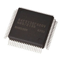
Renesas H8S/2300 Series Hardware Manual (875 pages)
16-Bit Single-Chip Microcomputer
Brand:
Renesas
| Category:
Computer Hardware
| Size: 5.48 MB
Table of Contents
General Precautions on Handling of Product
5
Preface
7
List of Registers
8
Register Bits
16
Table of Contents
21
Section 1 Overview
53
Features
53
Figure 1.1 Internal Block Diagram of H8S/2367, H8S/2365, and H8S/2363
55
Block Diagram
55
Figure
55
Figure 1.2 Internal Block Diagram of H8S/2366
56
Pin Description
57
Pin Arrangement
57
Figure 1.3 Pin Arrangement of H8S/2367, H8S/2365, and H8S/2363
57
Figure 1.4 Pin Arrangement of H8S/2366
58
Figure 1.5 Pin Arrangement of H8S/2367, H8S/2365, and H8S/2363
59
Figure 1.6 Pin Arrangement of H8S/2366
60
Pin Arrangement in each Operating Mode
61
Table 1.1 Pin Arrangement in each Operating Mode
61
Manual
62
Pin Functions
66
Table 1.2 Pin Functions
66
Section 2 CPU
73
Features
73
Differences between H8S/2600 CPU and H8S/2000 CPU
74
Differences from H8/300 CPU
75
Differences from H8/300H CPU
75
CPU Operating Modes
76
Normal Mode
76
Advanced Mode
77
Figure 2.1 Exception Vector Table (Normal Mode)
77
Figure 2.2 Stack Structure in Normal Mode
77
Figure 2.3 Exception Vector Table (Advanced Mode)
78
Figure 2.4 Stack Structure in Advanced Mode
79
Figure 2.5 Memory Map
80
Address Space
80
Figure 2.6 CPU Internal Registers
81
Figure 2.7 Usage of General Registers
82
General Registers
82
Extended Control Register (EXR)
83
Program Counter (PC)
83
Stack
83
Condition-Code Register (CCR)
84
Initial Register Values
86
Register Configuration
81
Data Formats
86
Figure 2.9 General Register Data Formats (1)
86
General Register Data Formats
86
Figure 2.9 General Register Data Formats (2)
87
Figure 2.10 Memory Data Formats
88
Memory Data Formats
88
Table 2.1
89
Table 2.2 Operation Notation
90
Table of Instructions Classified by Function
90
Table 2.3 Data Transfer Instructions
91
Table 2.4 Arithmetic Operations Instructions
92
Table 2.5 Logic Operations Instructions
94
Table 2.6 Shift Instructions
94
Table 2.7 Bit Manipulation Instructions
95
Table 2.8 Branch Instructions
97
Table 2.9 System Control Instructions
98
Basic Instruction Formats
99
Table 2.10 Block Data Transfer Instructions
99
Instruction Set
89
Table 2.11 Addressing Modes
100
Absolute Address-@Aa:8, @Aa:16, @Aa:24, or @Aa:32
101
Register Direct-Rn
101
Register Indirect with Displacement-@(D:16, Ern) or @(D:32, Ern)
101
Register Indirect with Post-Increment or Pre-Decrement-@Ern+ or @-Ern
101
Register Indirect-@Ern
101
Immediate-#XX:8, #XX:16, or #XX:32
102
Memory Indirect-@@Aa:8
102
Program-Counter Relative-@(D:8, PC) or @(D:16, PC)
102
Table 2.12 Absolute Address Access Ranges
102
Effective Address Calculation
103
Figure 2.12 Branch Address Specification in Memory Indirect Addressing Mode
103
Table 2.13 Effective Address Calculation
104
Figure 2.11 Instruction Formats (Examples)
100
Addressing Modes and Effective Address Calculation
100
Processing States
106
Usage Note
107
Note on Bit Manipulation Instructions
107
Figure 2.13 State Transitions
107
Section 3 MCU Operating Modes
109
Operating Mode Selection
109
Register Descriptions
110
Mode Control Register (MDCR)
110
System Control Register (SYSCR)
110
Operating Mode Descriptions
112
Mode 1
112
Mode 2
112
Mode 3
112
Mode 4
112
Mode 7
113
Pin Functions
113
Table 3.2 Pin Functions in each Operating Mode
113
Memory Map in each Operating Mode
114
Figure 3.1 H8S/2367 Memory Map (1)
114
Figure 3.2 H8S/2367 Memory Map (2)
115
Figure 3.3 H8S/2366 Memory Map (1)
116
Figure 3.4 H8S/2366 Memory Map (2)
117
Figure 3.5 H8S/2365 Memory Map (1)
118
Figure 3.6 H8S/2365 Memory Map (2)
119
Figure 3.7 H8S/2363 Memory Map
120
Section 4 Exception Handling
121
Table 4.1 Exception Types and Priority
121
Exception Handling Types and Priority
121
Exception Sources and Exception Vector Table
121
Table 4.2 Exception Handling Vector Table
122
Reset
123
Reset Exception Handling
123
Figure 4.1 Reset Sequence (Advanced Mode with On-Chip ROM Enabled)
124
Interrupts after Reset
125
On-Chip Peripheral Functions after Reset Release
125
Figure 4.2 Reset Sequence (Advanced Mode with On-Chip ROM Disabled)
125
Table 4.3 Status of CCR and EXR after Trace Exception Handling
126
Traces
126
Interrupts
126
Table 4.4 Status of CCR and EXR after Trap Instruction Exception Handling
127
Trap Instruction
127
Stack Status after Exception Handling
128
Figure 4.3 Stack Status after Exception Handling
128
Usage Notes
129
Figure 4.4 Operation When SP Value Is Odd
129
Section 5 Interrupt Controller
131
Features
131
Figure 5.1 Block Diagram of Interrupt Controller
132
Table 5.1 Pin Configuration
133
Interrupt Control Register (INTCR)
134
Interrupt Priority Registers a to K (IPRA to IPRK)
134
IRQ Enable Register (IER)
136
IRQ Sense Control Register L (ISCRL)
137
IRQ Status Register (ISR)
140
IRQ Pin Select Register (ITSR)
141
Software Standby Release IRQ Enable Register (SSIER)
142
Input/Output Pins
133
Register Descriptions
133
Interrupt Sources
142
External Interrupts
142
Internal Interrupts
143
Figure 5.2 Block Diagram of Interrupts IRQ15 to IRQ0
143
Interrupt Exception Handling Vector Table
144
Table 5.2 Interrupt Sources, Vector Addresses, and Interrupt Priorities
145
Interrupt Control Modes and Interrupt Operation
149
Interrupt Control Mode 0
149
Table 5.3 Interrupt Control Modes
149
Figure 5.3 Flowchart of Procedure up to Interrupt Acceptance
150
Interrupt Control Mode 2
151
Interrupt Exception Handling Sequence
152
Figure 5.4 Flowchart of Procedure up to Interrupt Acceptance in Interrupt Control Mode 2
152
Figure 5.5 Interrupt Exception Handling
153
Interrupt Response Times
154
Table 5.4 Interrupt Response Times
154
Table 5.5 Number of States in Interrupt Handling Routine Execution Statuses
154
DTC and DMAC* Activation by Interrupt
155
Usage Notes
155
Contention between Interrupt Generation and Disabling
155
Instructions that Disable Interrupts
156
Times When Interrupts Are Disabled
156
Interrupts During Execution of EEPMOV Instruction
156
Figure 5.6 Contention between Interrupt Generation and Disabling
156
Change of IRQ Pin Select Register (ITSR) Setting
157
Note on IRQ Status Register (ISR)
157
Section 6 Bus Controller (BSC)
159
Features
159
Figure 6.1 Block Diagram of Bus Controller
160
Input/Output Pins
161
Table 6.1 Pin Configuration
161
Register Descriptions
162
Bus Width Control Register (ABWCR)
163
Access State Control Register (ASTCR)
163
Wait Control Registers AH, AL, BH, and BL (WTCRAH, WTCRAL, WTCRBH, and WTCRBL)
164
Read Strobe Timing Control Register (RDNCR)
169
Figure 6.2 Read Strobe Negation Timing (Example of 3-State Access Space)
169
CS Assertion Period Control Registers H, L (CSACRH, CSACRL)
170
Figure 6.3 CS and Address Assertion Period Extension (Example of 3-State Access Space and Rdnn = 0)
171
Area 0 Burst ROM Interface Control Register (BROMCRH) Area 1 Burst ROM Interface Control Register (BROMCRL)
172
Bus Control Register (BCR)
173
DRAM Control Register (DRAMCR)
175
Figure 6.4 RAS Signal Assertion Timing
179
DRAM Access Control Register (DRACCR)
180
Refresh Control Register (REFCR)
181
Refresh Timer Counter (RTCNT)
184
Refresh Time Constant Register (RTCOR)
184
Operation
184
Area Division
184
Figure 6.5 Area Divisions
185
Bus Specifications
186
Table 6.2 Bus Specifications for each Area (Basic Bus Interface)
187
Memory Interfaces
188
Chip Select Signals
189
Figure 6.6 Csn Signal Output Timing (N = 0 to 7)
189
Basic Bus Interface
190
Data Size and Data Alignment
190
Figure 6.7 Access Sizes and Data Alignment Control (8-Bit Access Space)
190
Valid Strobes
191
Figure 6.8 Access Sizes and Data Alignment Control (16-Bit Access Space)
191
Table 6.3 Data Buses Used and Valid Strobes
191
Basic Timing
192
Figure 6.9 Bus Timing for 8-Bit, 2-State Access Space
192
Figure 6.10 Bus Timing for 8-Bit, 3-State Access Space
193
Figure 6.11 Bus Timing for 16-Bit, 2-State Access Space (Even Address Byte Access)
194
Figure 6.12 Bus Timing for 16-Bit, 2-State Access Space (Odd Address Byte Access)
195
Figure 6.13 Bus Timing for 16-Bit, 2-State Access Space (Word Access)
196
Figure 6.14 Bus Timing for 16-Bit, 3-State Access Space (Even Address Byte Access)
197
Figure 6.15 Bus Timing for 16-Bit, 3-State Access Space (Odd Address Byte Access)
198
Figure 6.16 Bus Timing for 16-Bit, 3-State Access Space (Word Access)
199
Wait Control
200
Read Strobe (RD) Timing
201
Figure 6.17 Example of Wait State Insertion Timing
201
Extension of Chip Select (CS) Assertion Period
202
Figure 6.18 Example of Read Strobe Timing
202
Figure 6.19 Example of Timing When Chip Select Assertion Period Is Extended
203
DRAM Interface
204
Setting DRAM Space
204
Address Multiplexing
204
Table 6.4 Relation between Settings of Bits RMTS2 to RMTS0 and DRAM Space
204
Data Bus
205
Table 6.5 Relation between Settings of Bits MXC2 to MXC0 and Address Multiplexing
205
Pins Used for DRAM Interface
206
Table 6.6 DRAM Interface Pins
206
Basic Timing
207
Figure 6.20 DRAM Basic Access Timing (RAST = 0, CAST = 0)
207
Column Address Output Cycle Control
208
Row Address Output State Control
208
Figure 6.21 Example of Access Timing with 3-State Column Address Output Cycle (RAST = 0)
208
Figure 6.22 Example of Access Timing When RAS Signal Goes Low from Beginning of T State (CAST = 0)
209
Figure 6.23 Example of Timing with One Row Address Output Maintenance State (RAST = 0, CAST = 0)
210
Precharge State Control
211
Figure 6.24 Example of Timing with Two-State Precharge Cycle (RAST = 0, CAST = 0)
211
Wait Control
212
Figure 6.25 Example of Wait State Insertion Timing (2-State Column Address Output)
213
Figure 6.26 Example of Wait State Insertion Timing (3-State Column Address Output)
214
Byte Access Control
215
Figure 6.27 2-CAS Control Timing (Upper Byte Write Access: RAST = 0, CAST = 0)
215
Burst Operation
216
Figure 6.28 Example of 2-CAS DRAM Connection
216
Figure 6.29 Operation Timing in Fast Page Mode (RAST = 0, CAST = 0)
217
Figure 6.30 Operation Timing in Fast Page Mode (RAST = 0, CAST = 1)
218
Figure 6.31 Example of Operation Timing in RAS down Mode (RAST = 0, CAST = 0)
219
Refresh Control
220
Figure 6.32 Example of Operation Timing in RAS up Mode (RAST = 0, CAST = 0)
220
Figure 6.33 RTCNT Operation
221
Figure 6.34 Compare Match Timing
221
Figure 6.35 CBR Refresh Timing
222
Figure 6.36 CBR Refresh Timing (RCW1 = 0, RCW0 = 1, RLW1 = 0, RLW0 = 0)
222
Figure 6.37 Example of CBR Refresh Timing (CBRM = 1)
223
Figure 6.38 Self-Refresh Timing
224
DMAC Single Address Transfer Mode and DRAM Interface
225
Figure 6.39 Example of Timing When Precharge Time after Self-Refreshing Is Extended by 2 States
225
Figure 6.40 Example of DACK Output Timing When DDS = 1 (RAST = 0, CAST = 0)
226
Figure 6.41 Example of DACK Output Timing When DDS = 0 (RAST = 0, CAST = 1)
227
Burst ROM Interface
228
Basic Timing
228
Figure 6.42 Example of Burst ROM Access Timing (Astn = 1, 2-State Burst Cycle)
229
Wait Control
230
Write Access
230
Figure 6.43 Example of Burst ROM Access Timing (Astn = 0, 1-State Burst Cycle)
230
Idle Cycle
231
Operation
231
Figure 6.44 Example of Idle Cycle Operation (Consecutive Reads in Different Areas)
231
Figure 6.45 Example of Idle Cycle Operation (Write after Read)
232
Figure 6.46 Example of Idle Cycle Operation (Read after Write)
233
Figure 6.47 Relationship between Chip Select (CS) and Read (RD)
234
Figure 6.48 Example of DRAM Full Access after External Read (CAST = 0)
234
Figure 6.49 Example of Idle Cycle Operation in RAS down Mode (Consecutive Reads in Different Areas) (IDLC = 0, RAST = 0, CAST = 0)
235
Figure 6.50 Example of Idle Cycle Operation in RAS down Mode (Write after Read) (IDLC = 0, RAST = 0, CAST = 0)
235
Figure 6.51 Example of Idle Cycle Operation after DRAM Access (Consecutive Reads in Different Areas) (IDLC = 0, RAST = 0, CAST = 0)
236
Figure 6.52 Example of Idle Cycle Operation after DRAM Access (Write after Read) (IDLC = 0, RAST = 0, CAST = 0)
237
Figure 6.53 Example of Idle Cycle Operation after DRAM Write Access (IDLC = 0, ICIS1 = 0, RAST = 0, CAST = 0)
238
Table 6.7 Idle Cycles in Mixed Accesses to Normal Space and DRAM
239
Figure 6.54 Example of Timing for Idle Cycle Insertion in Case of Consecutive Read
240
Pin States in Idle Cycle
241
Write Data Buffer Function
241
Table 6.8 Pin States in Idle Cycle
241
Bus Release
242
Operation
242
Figure 6.55 Example of Timing When Write Data Buffer Function Is Used
242
Pin States in External Bus Released State
244
Table 6.9 Pin States in Bus Released State
244
Transition Timing
245
Figure 6.56 Bus Released State Transition Timing
245
Bus Arbitration
246
Operation
246
Bus Transfer Timing
247
Bus Controller Operation in Reset
248
Usage Notes
248
External Bus Release Function and All-Module-Clocks-Stopped Mode
248
External Bus Release Function and Software Standby
248
External Bus Release Function and CBR Refreshing
248
BREQO Output Timing
249
Section 7 DMA Controller (DMAC)
251
Features
251
Figure 7.1 Block Diagram of DMAC
252
Register Descriptions
253
Table 7.1 Pin Configuration
253
Memory Address Registers (MARA and MARB)
254
Table 7.2 Short Address Mode and Full Address Mode (Channel 0)
254
Execute Transfer Count Registers (ETCRA and ETCRB)
255
I/O Address Registers (IOARA and IOARB)
255
DMA Control Registers (DMACRA and DMACRB)
256
DMA Band Control Registers H and L (DMABCRH and DMABCRL)
263
DMA Write Enable Register (DMAWER)
275
Figure 7.2 Areas for Register Re-Setting by DTC (Channel 0A)
276
DMA Terminal Control Register (DMATCR)
277
Input/Output Pins
253
Activation Sources
278
Activation by Internal Interrupt Request
278
Table 7.3 DMAC Activation Sources
278
Activation by External Request
279
Activation by Auto-Request
279
Operation
280
Transfer Modes
280
Table 7.4 DMAC Transfer Modes
280
Sequential Mode
282
Table 7.5 Register Functions in Sequential Mode
282
Figure 7.3 Operation in Sequential Mode
283
Idle Mode
284
Figure 7.4 Example of Sequential Mode Setting Procedure
284
Figure 7.5 Operation in Idle Mode
285
Table 7.6 Register Functions in Idle Mode
285
Repeat Mode
286
Figure 7.6 Example of Idle Mode Setting Procedure
286
Table 7.7 Register Functions in Repeat Mode
287
Figure 7.7 Operation in Repeat Mode
288
Single Address Mode
289
Figure 7.8 Example of Repeat Mode Setting Procedure
289
Table 7.8 Register Functions in Single Address Mode
290
Figure 7.9 Operation in Single Address Mode (When Sequential Mode Is Specified)
291
Normal Mode
292
Figure 7.10 Example of Single Address Mode Setting Procedure (When Sequential Mode Is Specified)
292
Table 7.9 Register Functions in Normal Mode
293
Figure 7.11 Operation in Normal Mode
294
Block Transfer Mode
295
Figure 7.12 Example of Normal Mode Setting Procedure
295
Table 7.10 Register Functions in Block Transfer Mode
296
Figure 7.13 Operation in Block Transfer Mode (BLKDIR = 0)
297
Figure 7.14 Operation in Block Transfer Mode (BLKDIR = 1)
298
Figure 7.15 Operation Flow in Block Transfer Mode
299
Figure 7.16 Example of Block Transfer Mode Setting Procedure
300
Basic Bus Cycles
301
DMA Transfer (Dual Address Mode) Bus Cycles
301
Figure 7.17 Example of DMA Transfer Bus Timing
301
Figure 7.18 Example of Short Address Mode Transfer
302
Figure 7.19 Example of Full Address Mode Transfer (Cycle Steal)
303
Figure 7.20 Example of Full Address Mode Transfer (Burst Mode)
304
Figure 7.21 Example of Full Address Mode Transfer (Block Transfer Mode)
305
Figure 7.22 Example of DREQ Pin Falling Edge Activated Normal Mode Transfer
306
Figure 7.23 Example of DREQ Pin Falling Edge Activated Block Transfer Mode Transfer
307
Figure 7.24 Example of DREQ Pin Low Level Activated Normal Mode Transfer
308
DMA Transfer (Single Address Mode) Bus Cycles
309
Figure 7.25 Example of DREQ Pin Low Level Activated Block Transfer Mode Transfer
309
Figure 7.26 Example of Single Address Mode Transfer (Byte Read)
310
Figure 7.27 Example of Single Address Mode (Word Read) Transfer
310
Figure 7.28 Example of Single Address Mode Transfer (Byte Write)
311
Figure 7.29 Example of Single Address Mode Transfer (Word Write)
312
Figure 7.30 Example of DREQ Pin Falling Edge Activated Single Address Mode Transfer
313
Figure 7.31 Example of DREQ Pin Low Level Activated Single Address Mode Transfer
314
Write Data Buffer Function
315
Figure 7.32 Example of Dual Address Transfer Using Write Data Buffer Function
315
Multi-Channel Operation
316
Figure 7.33 Example of Single Address Transfer Using Write Data Buffer Function
316
Table 7.11 DMAC Channel Priority Order
316
Relation between DMAC and External Bus Requests and Refresh Cycles
317
Figure 7.34 Example of Multi-Channel Transfer
317
DMAC and NMI Interrupts
318
Forced Termination of DMAC Operation
318
Figure 7.35 Example of Procedure for Continuing Transfer on Channel Interrupted
318
Clearing Full Address Mode
319
Figure 7.36 Example of Procedure for Forcibly Terminating DMAC Operation
319
Table 7.12 Interrupt Sources and Priority Order
320
Figure 7.37 Example of Procedure for Clearing Full Address Mode
320
Interrupt Sources
320
Usage Notes
321
DMAC Register Access During Operation
321
Figure 7.38 Block Diagram of Transfer End/Transfer Break Interrupt
321
Figure 7.39 DMAC Register Update Timing
322
Figure 7.40 Contention between DMAC Register Update and CPU Read
322
Module Stop
323
Write Data Buffer Function
323
TEND Output
323
Activation by Falling Edge on DREQ Pin
324
Figure 7.41 Example in Which Low Level Is Not Output at TEND Pin
324
Activation Source Acceptance
325
Internal Interrupt after End of Transfer
325
Channel Re-Setting
325
Section 8 Data Transfer Controller (DTC)
327
Features
327
Figure 8.1 Block Diagram of DTC
328
DTC Mode Register a (MRA)
329
DTC Destination Address Register (DAR)
330
DTC Mode Register B (MRB)
330
DTC Source Address Register (SAR)
330
DTC Transfer Count Register a (CRA)
330
DTC Enable Registers a to G (DTCERA to DTCERG)
331
DTC Transfer Count Register B (CRB)
331
DTC Vector Register (DTVECR)
331
Register Descriptions
328
Activation Sources
332
Location of Register Information and DTC Vector Table
333
Table 8.1 Relationship between Activation Sources and DTCER Clearing
333
Figure 8.2 Block Diagram of DTC Activation Source Control
333
Figure 8.3 Correspondence between DTC Vector Address and Register Information
334
Figure 8.4 Correspondence between DTC Vector Address and Register Information
334
Table 8.2 Interrupt Sources, DTC Vector Addresses, and Corresponding Dtces
335
Operation
336
Figure 8.5 Flowchart of DTC Operation
337
Normal Mode
338
Table 8.3 Chain Transfer Conditions
338
Table 8.4 Register Function in Normal Mode
338
Figure 8.6 Memory Mapping in Normal Mode
339
Repeat Mode
339
Table 8.5 Register Function in Repeat Mode
339
Block Transfer Mode
340
Figure 8.7 Memory Mapping in Repeat Mode
340
Table 8.6 Register Function in Block Transfer Mode
340
Chain Transfer
341
Figure 8.8 Memory Mapping in Block Transfer Mode
341
Figure 8.9 Operation of Chain Transfer
342
Interrupts
342
Figure 8.10 DTC Operation Timing (Example in Normal Mode or Repeat Mode)
343
Figure 8.11 DTC Operation Timing (Example of Block Transfer Mode, with Block Size of 2)
343
Figure 8.12 DTC Operation Timing (Example of Chain Transfer)
343
Operation Timing
343
Number of DTC Execution States
344
Table 8.7 DTC Execution Status
344
Table 8.8 Number of States Required for each Execution Status
344
Procedures for Using DTC
345
Activation by Interrupt
345
Activation by Software
345
Examples of Use of the DTC
345
Normal Mode
345
Chain Transfer
346
Chain Transfer When Counter = 0
347
Software Activation
348
Figure 8.13 Chain Transfer When Counter = 0
348
Usage Notes
349
Module Stop Mode Setting
349
On-Chip RAM
349
DTCE Bit Setting
349
DMAC Transfer End Interrupt
349
Chain Transfer
349
Section 9 I/O Ports
351
Table 9.1 Port Functions
352
Port 1
355
Port 1 Data Direction Register (P1DDR)
355
Port 1 Data Register (P1DR)
356
Port 1 Register (PORT1)
356
Pin Functions
357
Port 2
365
Port 2 Data Direction Register (P2DDR)
365
Port 2 Data Register (P2DR)
365
Port 2 Register (PORT2)
366
Pin Functions
367
Port 3
375
Port 3 Data Direction Register (P3DDR)
375
Port 3 Data Register (P3DR)
376
Port 3 Register (PORT3)
376
Port 3 Open Drain Control Register (P3ODR)
377
Port Function Control Register 2 (PFCR2)
378
Pin Functions
379
Port 4
382
Port 4 Register (PORT4)
382
Pin Functions
383
Port 5
385
Port 5 Data Direction Register (P5DDR)
385
Port 5 Data Register (P5DR)
385
Port 5 Register (PORT5)
386
Pin Functions
386
Port 8
388
Port 8 Data Direction Register (P8DDR)
388
Port 8 Data Register (P8DR)
389
Port 8 Register (PORT8)
389
Pin Functions
390
Port 9
391
Port 9 Register (PORT9)
391
Pin Functions
391
Port a
392
Port a Data Direction Register (PADDR)
393
Port a Data Register (PADR)
394
Port a Register (PORTA)
394
Port a MOS Pull-Up Control Register (PAPCR)
395
Port a Open Drain Control Register (PAODR)
395
Port Function Control Register 0 (PFCR0)
396
Port Function Control Register 1 (PFCR1)
396
Pin Functions
397
Port a MOS Input Pull-Up States
399
Table 9.2 MOS Input Pull-Up States (Port A)
399
Port B
400
Port B Data Direction Register (PBDDR)
400
Port B Data Register (PBDR)
401
Port B Register (PORTB)
401
Port B MOS Pull-Up Control Register (PBPCR)
402
Pin Functions
402
Port B MOS Input Pull-Up States
403
Table 9.3 MOS Input Pull-Up States (Port B)
403
Port C
404
Port C Data Direction Register (PCDDR)
404
Port C Data Register (PCDR)
405
Port C Register (PORTC)
405
Port C MOS Pull-Up Control Register (PCPCR)
406
Pin Functions
406
Port C MOS Input Pull-Up States
407
Table 9.4 MOS Input Pull-Up States (Port C)
407
Port D
408
Port D Data Direction Register (PDDDR)
408
Port D Data Register (PDDR)
408
Port D Register (PORTD)
409
Port D Pull-Up Control Register (PDPCR)
409
Pin Functions
410
Port D MOS Input Pull-Up States
410
Table 9.5 MOS Input Pull-Up States (Port D)
410
Port E
411
Port E Data Direction Register (PEDDR)
411
Port E Data Register (PEDR)
412
Port E Register (PORTE)
412
Port E Pull-Up Control Register (PEPCR)
413
Pin Functions
413
Port E MOS Input Pull-Up States
414
Port F
414
Table 9.6 MOS Input Pull-Up States (Port E)
414
Port F Data Direction Register (PFDDR)
415
Port F Data Register (PFDR)
416
Port F Register (PORTF)
416
Pin Functions
417
Port G
420
Port G Data Direction Register
420
Port G Data Register
422
Port G Register (PORTG)
422
Pin Functions
423
Section 10 16-Bit Timer Pulse Unit (TPU)
425
Features
425
Table 10.1 TPU Functions
426
Figure 10.1 Block Diagram of TPU
428
Table 10.2 Pin Configuration
429
Input/Output Pins
429
Register Descriptions
430
Timer Control Register (TCR)
432
Table 10.3 CCLR2 to CCLR0 (Channels 0 and 3)
433
Table 10.4 CCLR2 to CCLR0 (Channels 1, 2, 4, and 5)
433
Table 10.5 TPSC2 to TPSC0 (Channel 0)
434
Table 10.6 TPSC2 to TPSC0 (Channel 1)
434
Table 10.7 TPSC2 to TPSC0 (Channel 2)
435
Table 10.8 TPSC2 to TPSC0 (Channel 3)
435
Table 10.9 TPSC2 to TPSC0 (Channel 4)
436
Table 10.10 TPSC2 to TPSC0 (Channel 5)
436
Timer Mode Register (TMDR)
437
Timer I/O Control Register (TIOR)
438
Table 10.11 MD3 to MD0
438
Table 10.12 TIORH_0
440
Table 10.13 TIORL_0
441
Table 10.14 TIOR_1
442
Table 10.15 TIOR_2
443
Table 10.16 TIORH_3
444
Table 10.17 TIORL_3
445
Table 10.18 TIOR_4
446
Table 10.19 TIOR_5
447
Table 10.20 TIORH_0
448
Table 10.21 TIORL_0
449
Table 10.22 TIOR_1
450
Table 10.23 TIOR_2
451
Table 10.24 TIORH_3
452
Table 10.25 TIORL_3
453
Table 10.26 TIOR_4
454
Table 10.27 TIOR_5
455
Timer Interrupt Enable Register (TIER)
456
Timer Status Register (TSR)
458
Timer Counter (TCNT)
460
Timer General Register (TGR)
461
Timer Start Register (TSTR)
461
Timer Synchronous Register (TSYR)
462
Advertisement
Renesas H8S/2300 Series Hardware Manual (1047 pages)
16-Bit Single-Chip Microcomputer
Brand:
Renesas
| Category:
Computer Hardware
| Size: 4.54 MB
Table of Contents
Table of Contents
13
Section 1 Overview
29
Overview
29
Block Diagram
34
Pin Description
35
Pin Arrangement
35
Pin Functions in each Operating Mode
39
Pin Functions
43
Section 2 CPU
49
Overview
49
Features
49
Differences between H8S/2600 CPU and H8S/2000 CPU
50
Differences from H8/300 CPU
50
Differences from H8/300H CPU
51
CPU Operating Modes
51
Advanced Mode
51
Address Space
54
Register Configuration
55
Overview
55
General Registers
55
Control Registers
56
Initial Register Values
57
Data Formats
58
General Register Data Formats
58
Memory Data Formats
60
Instruction Set
61
Overview
61
Instructions and Addressing Modes
62
Table of Instructions Classified by Function
63
Basic Instruction Formats
69
Addressing Modes and Effective Address Calculation
69
Addressing Mode
69
Effective Address Calculation
72
Processing States
75
Overview
75
Reset State
76
Exception-Handling State
76
Program Execution State
78
Bus-Released State
78
Power-Down State
78
Basic Timing
79
Overview
79
On-Chip Memory (ROM, RAM)
79
On-Chip Supporting Module Access Timing
80
External Address Space Access Timing
81
Usage Note
81
TAS Instruction
81
Section 3 MCU Operating Modes
83
Overview
83
Operating Mode Selection (H8S/2357 F-ZTAT Only)
83
Operating Mode Selection (ZTAT, Masked ROM, Romless Version, and H8S/2398 F-ZTAT)
84
Register Configuration
85
Register Descriptions
85
Mode Control Register (MDCR)
85
System Control Register (SYSCR)
85
System Control Register 2 (SYSCR2) (F-ZTAT Version Only)
86
Operating Mode Descriptions
88
Mode 1
88
Mode 2 (H8S/2398 F-ZTAT Only)
88
Mode 3 (H8S/2398 F-ZTAT Only)
88
Mode 4 (On-Chip ROM Disabled Expansion Mode)
88
Mode 5 (On-Chip ROM Disabled Expansion Mode)
88
Mode 6 (On-Chip ROM Enabled Expansion Mode)
88
Mode 7 (Single-Chip Mode)
89
Modes 8 and 9
89
Mode 10 (H8S/2357 F-ZTAT Only)
89
Mode 11 (H8S/2357 F-ZTAT Only)
89
Modes 12 and 13 (H8S/2357 F-ZTAT Only)
89
Mode 14 (H8S/2357 F-ZTAT Only)
89
Mode 15 (H8S/2357 F-ZTAT Only)
89
Pin Functions in each Operating Mode
90
Memory Map in each Operating Mode
90
Section 4 Exception Handling
99
Overview
99
Exception Handling Types and Priority
99
Exception Handling Operation
100
Exception Vector Table
100
Reset
102
Overview
102
Reset Types
102
Reset Sequence
103
Interrupts after Reset
104
State of On-Chip Supporting Modules after Reset Release
104
Traces
104
Interrupts
105
Trap Instruction
106
Stack Status after Exception Handling
106
Notes on Use of the Stack
107
Section 5 Interrupt Controller
109
Overview
109
Features
109
Block Diagram
110
Pin Configuration
110
Register Configuration
111
Register Descriptions
111
System Control Register (SYSCR)
111
Interrupt Priority Registers a to K (IPRA to IPRK)
112
IRQ Enable Register (IER)
113
IRQ Sense Control Registers H and L (ISCRH, ISCRL)
114
IRQ Status Register (ISR)
114
Interrupt Sources
115
External Interrupts
115
Internal Interrupts
116
Interrupt Exception Handling Vector Table
116
Interrupt Operation
119
Interrupt Control Modes and Interrupt Operation
119
Interrupt Control Mode 0
121
Interrupt Control Mode 2
123
Interrupt Exception Handling Sequence
125
Interrupt Response Times
126
Usage Notes
127
Contention between Interrupt Generation and Disabling
127
Instructions that Disable Interrupts
127
Times When Interrupts Are Disabled
128
Interrupts During Execution of EEPMOV Instruction
128
DTC and DMAC Activation by Interrupt
128
Overview
128
Block Diagram
129
Operation
129
Note on Use
130
Section 6 Bus Controller
131
Overview
131
Features
131
Block Diagram
133
Pin Configuration
134
Register Configuration
135
Register Descriptions
136
Bus Width Control Register (ABWCR)
136
Access State Control Register (ASTCR)
137
Wait Control Registers H and L (WCRH, WCRL)
138
Bus Control Register H (BCRH)
141
Bus Control Register L (BCRL)
142
Memory Control Register (MCR)
144
DRAM Control Register (DRAMCR)
146
Refresh Timer/Counter (RTCNT)
147
Refresh Time Constant Register (RTCOR)
148
Overview of Bus Control
149
Area Partitioning
149
Bus Specifications
150
Memory Interfaces
151
Advanced Mode
151
Chip Select Signals
152
Basic Bus Interface
153
Overview
153
Data Size and Data Alignment
153
Valid Strobes
155
Basic Timing
156
Wait Control
164
DRAM Interface
166
Overview
166
Setting DRAM Space
166
Address Multiplexing
166
Data Bus
166
Pins Used for DRAM Interface
167
Basic Timing
168
Precharge State Control
169
Wait Control
169
Byte Access Control
171
Burst Operation
172
Refresh Control
175
DMAC Single Address Mode and DRAM Interface
177
When DDS = 1
177
When DDS = 0
178
Burst ROM Interface
178
Overview
178
Basic Timing
179
Wait Control
180
Idle Cycle
181
Operation
181
Usage Notes
183
Pin States in Idle Cycle
185
Write Data Buffer Function
186
Bus Release
187
Overview
187
Operation
187
Pin States in External Bus Released State
188
Transition Timing
189
Usage Note
189
Bus Arbitration
190
Overview
190
Operation
190
Bus Transfer Timing
191
External Bus Release Usage Note
191
Resets and the Bus Controller
192
Section 7 DMA Controller
193
Overview
193
Features
193
Block Diagram
194
Overview of Functions
195
Pin Configuration
197
Register Configuration
198
Register Descriptions (1) (Short Address Mode)
199
Memory Address Registers (MAR)
200
I/O Address Register (IOAR)
200
Execute Transfer Count Register (ETCR)
201
DMA Control Register (DMACR)
202
DMA Band Control Register (DMABCR)
205
Register Descriptions (2) (Full Address Mode)
209
Memory Address Register (MAR)
209
I/O Address Register (IOAR)
209
Execute Transfer Count Register (ETCR)
209
DMA Control Register (DMACR)
211
DMA Band Control Register (DMABCR)
214
Register Descriptions (3)
218
DMA Write Enable Register (DMAWER)
218
DMA Terminal Control Register (DMATCR)
220
Module Stop Control Register (MSTPCR)
221
Operation
222
Transfer Modes
222
Sequential Mode
224
Idle Mode
227
Repeat Mode
229
Single Address Mode
232
Normal Mode
235
Block Transfer Mode
238
DMAC Activation Sources
243
Basic DMAC Bus Cycles
245
DMAC Bus Cycles (Dual Address Mode)
246
DMAC Bus Cycles (Single Address Mode)
254
Write Data Buffer Function
258
DMAC Multi-Channel Operation
259
Relation between External Bus Requests, Refresh Cycles, the DTC, and the DMAC
260
NMI Interrupts and DMAC
261
Forced Termination of DMAC Operation
262
Clearing Full Address Mode
263
Interrupts
264
Usage Notes
265
Section 8 Data Transfer Controller
269
Overview
269
Features
269
Block Diagram
270
Register Configuration
271
Register Descriptions
272
DTC Mode Register a (MRA)
272
DTC Mode Register B (MRB)
273
DTC Source Address Register (SAR)
274
DTC Destination Address Register (DAR)
274
DTC Transfer Count Register a (CRA)
274
DTC Transfer Count Register B (CRB)
274
DTC Enable Registers (DTCER)
275
DTC Vector Register (DTVECR)
275
Module Stop Control Register (MSTPCR)
276
Operation
277
Overview
277
Activation Sources
279
DTC Vector Table
280
Location of Register Information in Address Space
283
Normal Mode
284
Repeat Mode
285
Block Transfer Mode
286
Chain Transfer
287
Operation Timing
288
Number of DTC Execution States
289
Procedures for Using DTC
290
Examples of Use of the D7TC
290
Interrupts
292
Usage Notes
292
Section 9 I/O Ports
293
Overview
293
Port1
297
Overview
297
Register Configuration
297
Pin Functions
299
Port2
307
Overview
307
Register Configuration
307
Pin Functions
309
Port 3
317
Overview
317
Register Configuration
317
Pin Functions
319
Port 4
321
Overview
321
Register Configuration
321
Pin Functions
321
Port 5
322
Overview
322
Register Configuration
322
Pin Functions
324
Port 6
325
Overview
325
Register Configuration
325
Pin Functions
327
Port a
329
Overview
329
Register Configuration
330
Pin Functions
332
MOS Input Pull-Up Function (On-Chip ROM Version Only)
334
Port B
335
Overview
335
Register Configuration (On-Chip ROM Version Only)
336
Pin Functions
338
MOS Input Pull-Up Function (On-Chip ROM Version Only)
339
Port C
340
Overview
340
Register Configuration (On-Chip ROM Version Only)
341
Pin Functions
343
MOS Input Pull-Up Function (On-Chip ROM Version Only)
344
Port D
345
Overview
345
Register Configuration (On-Chip ROM Version Only)
346
Pin Functions
348
MOS Input Pull-Up Function (On-Chip ROM Version Only)
349
Port E
350
Overview
350
Register Configuration
351
Pin Functions
353
MOS Input Pull-Up Function (On-Chip ROM Version Only)
354
Port F
355
Overview
355
Register Configuration
356
Pin Functions
358
Port G
360
Overview
360
Register Configuration
360
Pin Functions
363
Section 10 16-Bit Timer Pulse Unit (TPU)
365
Overview
365
Features
365
Block Diagram
369
Pin Configuration
370
Register Configuration
371
Register Descriptions
373
Timer Control Register (TCR)
373
Timer Mode Register (TMDR)
377
Timer I/O Control Register (TIOR)
379
Timer Interrupt Enable Register (TIER)
389
Timer Status Register (TSR)
391
Timer Counter (TCNT)
394
Timer General Register (TGR)
394
Timer Start Register (TSTR)
394
Timer Synchro Register (TSYR)
395
Module Stop Control Register (MSTPCR)
396
Interface to Bus Master
397
16-Bit Registers
397
8-Bit Registers
398
Operation
399
Overview
399
Basic Functions
400
Synchronous Operation
405
Buffer Operation
407
Cascaded Operation
410
PWM Modes
411
Phase Counting Mode
416
Interrupts
422
Interrupt Sources and Priorities
422
DTC/DMAC Activation
424
A/D Converter Activation
424
Operation Timing
425
Input/Output Timing
425
Interrupt Signal Timing
429
Usage Notes
432
Advertisement
Related Products
Renesas H8S/2378 Series
Renesas H8S/2328 Series
Renesas H8S/2345 Series
Renesas H8S/2338 Series
Renesas H8S/2319 series
Renesas H8S/2318 series
Renesas H8S/2368 Series
Renesas F-ZTAT H8S/2357F
Renesas H8S/2357 Series
Renesas ZTAT H8S/2398F
Renesas Categories
Computer Hardware
Motherboard
Microcontrollers
Adapter
Switch
More Renesas Manuals
Login
Sign In
OR
Sign in with Facebook
Sign in with Google
Upload manual
Upload from disk
Upload from URL