Analog Devices ADSP-21261 SHARC Processor Manuals
Manuals and User Guides for Analog Devices ADSP-21261 SHARC Processor. We have 2 Analog Devices ADSP-21261 SHARC Processor manuals available for free PDF download: Hardware Reference Manual, Getting Started Manual
Analog Devices ADSP-21261 SHARC Hardware Reference Manual (846 pages)
Brand: Analog Devices
|
Category: Computer Hardware
|
Size: 11 MB
Table of Contents
-
Preface
31 -
Introduction
41 -
-
-
-
Bus Conflicts117
-
Block Conflicts119
-
Using the Cache120
-
-
-
Delayed Branches125
-
Core Stalls133
-
Execution Stalls135
-
DAG Stalls136
-
Memory Stalls136
-
DMA Stalls136
-
-
-
Summary173
-
-
Using DAG Status187
-
DAG Operations187
-
Memory
205-
Internal Memory206
-
DSP Architecture206
-
-
Buses207
-
-
Accessing Memory226
-
Access Word Size227
-
-
-
-
-
Boundary Scan282
-
References289
-
I/O Processor
292-
Address Register302
-
Parallel Port
323 -
Serial Ports
351-
-
I 2 S Mode368
-
-
Word Length389
-
Endian Format390
-
Data Type391
-
Companding392
-
-
-
-
-
SPI Enable444
-
-
-
Spi Dma448
-
DMA Chaining461
-
SPI Word Lengths465
-
Packing467
-
SPI Interrupts468
-
SPI Registers470
-
-
Serial Inputs493
-
-
Masking498
-
Packing Unit498
-
Packing Mode 11499
-
Packing Mode 01500
-
Packing Mode 00501
-
-
PDAP Strobe503
-
-
-
-
-
Clock Outputs557
-
Phase Shift561
-
Pulse Width563
-
Bypass Mode564
-
-
-
-
Timer Interrupts574
-
-
Enabling a Timer575
-
15 System Design
591-
Pin Descriptions592
-
Booting609
-
SPI Port Booting612
-
-
-
-
-
-
SPI Registers714
-
Shift Registers722
-
-
-
-
DAI Registers783
-
-
Interrupt Vector
797
Advertisement
Analog Devices ADSP-21261 SHARC Getting Started Manual (114 pages)
SHARC Series
Brand: Analog Devices
|
Category: Computer Hardware
|
Size: 2 MB
Table of Contents
-
Preface
9 -
-
-
-
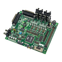
EZ-KIT Lite42
-
EZ-Board43
-
EZ-Boards66
-
Debug Agent76
-
Scenario 190
-
Scenario 291
-
-
-
-
-
Visualdsp++ Help106
-
Engineerzone107
-
Myanalog.com108
-
Advertisement
Related Products
- Analog Devices ADSP-21262 SHARC
- Analog Devices ADSP-21266 SHARC
- Analog Devices ADSP-21267 SHARC
- Analog Devices ADSP-2181
- Analog Devices ADSP-2183
- Analog Devices EZ-KIT Lite ADSP-21364
- Analog Devices EZ-KIT LITE ADSP-2191
- Analog Devices SHARC ADSP-21367
- Analog Devices SHARC ADSP-21368
- Analog Devices SHARC ADSP-21363