Sign In
Upload
Manuals
Brands
Analog Devices Manuals
Computer Hardware
SHARC ADSP-21367
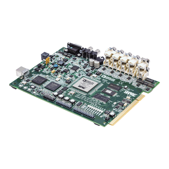
Analog Devices SHARC ADSP-21367 Manuals
Manuals and User Guides for Analog Devices SHARC ADSP-21367. We have
3
Analog Devices SHARC ADSP-21367 manuals available for free PDF download: Hardware Reference Manual, Getting Started Manual, Manual
Analog Devices SHARC ADSP-21367 Hardware Reference Manual (894 pages)
Brand:
Analog Devices
| Category:
Computer Hardware
| Size: 4 MB
Table of Contents
Table of Contents
3
Preface
31
Purpose of this Manual
31
Intended Audience
31
Manual Contents
32
What's New in this Manual
34
Technical or Customer Support
35
Supported Processors
36
Product Information
36
Myanalog.com
37
Processor Product Information
37
Related Documents
38
Online Technical Documentation
39
Printed Manuals
41
Conventions
43
Introduction
45
Design Advantages
45
Architectural Overview
50
Processor Core
51
Processor Peripherals
51
I/O Processor
51
Digital Audio Interface (DAI)
53
Digital Peripheral Interface (DPI)
54
Development Tools
54
Differences from Previous Processors
55
I/O Architecture Enhancements
55
Instruction Set Enhancements
56
General Procedure for Configuring DMA
58
Core Access to IOP Registers
59
Configuring Iop/Core Interaction
62
Interrupt-Driven I/O
62
Interrupt Latency in Interrupt-Driven Transfers
67
Polling/Status-Driven I/O
68
DMA Controller Operation
69
Chaining DMA Processes
70
Transfer Control Block Chain Loading (TCB)
72
Setting up DMA Channel Allocation and Priorities
74
Managing DMA Channel Priority
75
DMA Bus Arbitration
76
Setting up DMA Parameter Registers
80
DMA Transfer Direction
80
Data Buffer Registers
81
Port, Buffer, and DMA Control Registers
82
Addressing
85
External Port DMA
91
Setting up and Starting Chained DMA
92
Delay Line DMA
94
Serial Port DMA
96
Setting up and Starting Chained DMA
96
Inserting a TCB in an Active Chain
97
Serial Peripheral Interface DMA
98
Setting up and Starting Chained DMA over the SPI
98
Uart Dma
100
Notes on Using DMA with the UART
103
Memory-To-Memory DMA
104
Summary
104
Programming Example
105
External Port
109
External Memory Interface
110
External Memory Interface on the ADSP-2137X Processors
111
Direct Execution of Instructions from External Memory
111
Throughput and Instruction Execution Rate
111
Location of Interrupt Vector Table (IVT)
112
Instruction Cache
113
Instruction Storage and Packing
117
Register Configurations for External Memory Execution
123
EMI Registers and Signals
124
External Port Arbitration Logic
126
Channel Freezing
126
Managing Data Paths
126
External Memory Interface Pins
127
Asynchronous Memory Interface
128
AMI Timing Control
129
Wait States
129
Bus Idle Cycles
130
Bus Hold Cycles
131
Setting AMI Modes
132
External Memory Reads
133
Data Packing
133
External Memory Writes
134
Data Packing
135
Read/Write Throughput
136
External Access Addressing
136
External Port DMA
138
Booting through the AMI
138
SDRAM Controller
138
Definition of Terms
139
Timing External Memory Accesses
144
Parallel Connection of Sdrams
147
SDRAM Control Register (SDCTL)
147
SDRAM Control Status Register (SDSTAT)
157
SDRAM Refresh Rate Control Register (SDRRC)
157
SDRAM Initialization
159
SDRAM Address Mapping
159
SDRAM Controller Address Mapping
166
SDC Operation
166
Single Bank Operation
168
Multibank Operation (ADSP-2137X Processors)
168
Data Mask (DQM)
169
SDC Configuration
169
SDC Commands
171
Load Mode Register
172
Single Bank Activation
173
Multibank Activation (ADSP-2137X Processors)
174
Single Precharge (ADSP-2137X Processors)
174
Precharge All
174
Read/Write
175
Read/Write (ADSP-2137X Processors)
177
Burst Stop (ADSP-2137X Processors)
177
Auto-Refresh
178
Self-Refresh Mode
178
No Operation/Command Inhibit
179
Changing System Clock During Runtime
181
SDRAM Timing
182
SDRAM Read Optimization
183
External Memory Access Restrictions
186
Shared Memory Interface
187
Shared Memory Bus Arbitration
187
Bus Arbitration Protocol
190
Bus Arbitration Priority (RPBA)
194
Bus Mastership Time-Out
195
Bus Synchronization after Reset
196
Bus Synchronization Notes
199
Bus Lock and Semaphores
200
Shared Memory Interface Status
201
Shared Memory and the SDRAM Controller
202
Shared Memory Booting
202
Digital Audio/Digital Peripheral Interfaces
203
Structure of the Interfaces
204
DAI/DPI System Design
205
Signal Routing Units
210
Connecting Peripherals
210
Pin Interface
212
Pin Buffers as Signal Output Pins
213
Pin Buffers as Signal Input Pins
214
Bidirectional Pin Buffers
215
Making Connections in the Srus
217
DAI/SRU1 Connection Groups
220
Group a Connections-Clock Signals
221
Group B Connections-Data Signals
227
Group C Connections-Frame Sync Signals
233
Group D Connections-Pin Signal Assignments
238
Group E Connections-Interrupts and Miscellaneous Signals
245
Group F-Pin Enable Signals
249
DPI/SRU2 Connection Groups
253
Group a Connections-Input Routing Signals
254
Group B Connections-Pin Assignment Signals
258
Group C Connections-Pin Enable Signals
262
DAI GPIO and Flags
266
DPI GPIO and Flags
267
Miscellaneous Signals
267
DAI/DPI Interrupt Controller
267
Relationship to the Core
267
DAI Interrupts
268
DPI Interrupts
269
High and Low Priority Latches
271
Rising and Falling Edge Masks
272
Configuring the SPI
274
Choosing the Pin Enable for the SPI Clock
274
Configuring the Two Wire Interface
275
Using the SRU() Macro to Configure the DAI
278
Serial Ports
281
Features
282
Operation Modes
283
Serial Port Signals
285
Serial Port Signal Sensitivity
289
SPORT Operation Modes
290
Standard DSP Serial Mode
291
Standard DSP Serial Mode Control Bits
293
Clocking Options
293
Frame Sync Options
293
Data Formatting
294
Data Transfers
295
Status Information
295
Left-Justified Sample Pair Mode
296
Setting the Internal Serial Clock and Frame Sync Rates
297
Left-Justified Sample Pair Mode Control Bits
297
Setting Word Length (SLEN)
297
Enabling SPORT Master Mode (MSTR)
298
Selecting Transmit and Receive Channel Order (FRFS)
298
Selecting Frame Sync Options (DIFS)
298
Enabling SPORT DMA (SDEN)
299
I2S Mode
300
Setting the Internal Serial Clock and Frame Sync Rates
301
I2S Mode Control Bits
301
Setting Word Length (SLEN)
302
Enabling SPORT Master Mode (MSTR)
303
Selecting Transmit and Receive Channel Order (FRFS)
303
Selecting Frame Sync Options (DIFS)
303
Enabling SPORT DMA (SDEN)
304
Multichannel Operation
305
Frame Syncs in Multichannel Mode
308
Multichannel Mode Control Bits
309
Packed I2S Mode
313
SPORT Loopback
315
Clock Signal Options
316
Frame Sync Options
317
Framed Versus Unframed Frame Syncs
317
Internal Versus External Frame Syncs
318
Active Low Versus Active High Frame Syncs
319
Sampling Edge for Data and Frame Syncs
319
Early Versus Late Frame Syncs
320
Data-Independent Frame Syncs
321
Frame Sync Error Detection
322
Data Word Formats
323
Word Length
323
Endian Format
325
Data Packing and Unpacking
325
Data Type
326
Companding
327
SPORT Control Registers and Data Buffers
329
Serial Port Control Registers (Spctlx)
339
Transmit and Receive Data Buffers (Txspxa/B, Rxspxa/B)
347
Clock and Frame Sync Frequency Registers (DIVX)
349
SPORT Reset
351
SPORT Interrupts
352
Moving Data between Sports and Internal Memory
353
DMA Block Transfers
353
Setting up DMA on SPORT Channels
355
SPORT DMA Parameter Registers
356
SPORT DMA Chaining
361
Single Word Transfers
361
SPORT Programming Examples
362
Serial Peripheral Interface Ports
373
Functional Description
374
SPI Interface Signals
376
SPI Clock Signal (SPICLK)
376
SPICLK Timing
377
SPI Flag Signals (SPIFLG3-0)
378
Master out Slave in (MOSI)
379
Master in Slave out (MISO)
379
SPI General Operations
380
SPI Enable
381
Open Drain Mode (OPD)
381
Master Mode Operation
382
Slave Mode Operation
383
Multimaster Operation
384
SPI Data Transfer Operations
385
SPI Operation Using the Core
385
SPI Operation Using DMA
386
Master Mode DMA Operation
387
Slave Mode DMA Operation
391
Changing SPI Configuration
393
Switching from Transmit to Receive DMA
395
Switching from Receive to Transmit DMA
396
DMA Error Interrupts
397
DMA Chaining
399
SPI Transfer Formats
399
Beginning and Ending an SPI Transfer
401
SPI Word Lengths
403
16-Bit Word Lengths
404
Packing
404
SPI Interrupts
405
Error Signals and Flags
407
Mode Fault Error (MME)
407
Transmission Error Bit (TUNF)
409
Reception Error Bit (ROVF)
409
Transmit Collision Error Bit (TXCOL)
409
Programming Notes
410
Routing SPI Signals Using the DPI
410
Programming Examples
410
Input Data Port
419
Serial Inputs
421
Parallel Data Acquisition Port (PDAP)
421
Masking
427
Packing Mode 11
428
Packing Mode 10
429
Packing Mode 01
429
Packing Mode 00
430
Clocking Edge Selection
430
Hold Input
430
PDAP Strobe
432
FIFO Control and Status
433
FIFO to Memory Data Transfer
434
IDP Transfers Using the Core
435
Starting an Interrupt-Driven Transfer
436
IDP Transfers Using DMA
438
Simple DMA
438
Ping-Pong DMA
440
DMA Transfer Notes
443
DMA Channel Parameter Registers
445
IDP (DAI) Interrupt Service Routines for Dmas
446
FIFO Overflow
448
Input Data Port Programming Example
449
Pulse Width Modulation
453
PWM Implementation
453
Edge-Aligned Mode
454
Center-Aligned Mode
455
Switching Frequencies
457
Dead Time
458
Duty Cycles
459
Duty Cycles and Dead Time
460
Over Modulation
464
Update Modes
467
Single Update
467
Configurable Polarity
467
PWM Pins and Signals
468
Crossover
468
PWM Accuracy
469
PWM Registers
470
Duty Cycles
471
Output Enable
472
Programming Example
473
AES3/SPDIF Stream Format
478
Subframe Format
479
Channel Coding
481
Preambles
482
S/PDIF Transmitter
483
Channel Status
485
SRU1 Signals for the S/PDIF Transmitter
486
Modes of Operation
488
Standalone Mode
489
Structure of the Serial Input Data
490
S/PDIF Receiver
492
S/PDIF Receiver Registers
493
SRU1 Receiver Signals
494
Phase-Locked Loop
495
Channel Status Decoding
495
Compressed or Non-Linear Audio Data
496
Emphasized Audio Data
497
Single-Channel, Double-Sampling Frequency Mode
497
Error Handling
498
Interrupts
500
DAI Programming Examples
500
Control Register
500
SRU1 Programming for Input and Output Streams
501
Control Register Programming and Enable
501
S/PDIF Receiver Programming Guidelines
501
Control Register
501
SRU1 Programming
502
Control Register Programming
502
Receiver Locking
502
Status Bits
502
Interrupted Data Streams on the Receiver
503
Asynchronous Sample Rate Converter
505
Theory of Operation
506
Conceptual Model
508
Hardware Model
511
Sample Rate Converter Architecture
512
Group Delay
516
SRC Operation
516
Enabling the SRC
517
Serial Data Ports
517
Data Format
517
Time-Division Multiplex (TDM) Output Mode
519
TDM Input Mode
520
Matched-Phase Mode
520
Bypass Mode
522
De-Emphasis Filter
522
Mute Control
523
Soft Mute
524
Hard Mute
524
Auto Mute
524
SRC Registers
525
Programming the SRC Module
526
SRC Control Register Programming
526
SRU Programming
526
SRC Mute-Out Interrupt
527
Sample Rate Ratio
527
Programming Summary
527
11 Uart Port Controller
529
Serial Communications
530
UART Control and Status Registers
531
Uartxlcr Registers
531
Uartxlsr Register
532
Uartxthr Register
532
Uartxrbr Register
533
Uartxier Register
535
Uartxiir Register
537
Uartxdll and Uartxdlh Registers
539
Uartxscr Register
540
Uartxmode Register
541
I/O Mode
541
Packing Mode
543
Two Wire Interface Controller
545
Overview
545
Architecture
546
Register Descriptions
548
TWI Master Internal Time Register
548
TWIDIV Register
549
Slave Mode Control Register
549
Slave Mode Address Register
550
Slave Mode Status Register
550
Master Mode Control Register
550
Master Mode Address Register
550
Master Mode Status Register
551
FIFO Control Register
551
FIFO Status Register
551
Interrupt Source Register
551
Interrupt Enable Register
552
16-Bit Transmit FIFO Register
552
8-Bit Receive FIFO Register
553
16-Bit Receive FIFO Register
554
Data Transfer Mechanics
554
Clock Generation and Synchronization
555
Bus Arbitration
556
General Call Support
558
Fast Mode
558
Programming Examples
559
General Setup
559
Slave Mode
559
Master Mode Clock Setup
561
Master Mode Transmit
561
Master Mode Receive
562
Repeated Start Condition
563
Transmit/Receive Repeated Start Sequence
563
Receive/Transmit Repeated Start Sequence
565
Electrical Specifications
566
Precision Clock Generators
567
Clock Outputs
569
Frame Sync Outputs
570
Normal Mode
571
Bypass Mode
572
Frame Sync Output Synchronization with an External Clock
573
Frame Sync
574
Phase Shift
575
Phase Shift Settings
576
Pulse Width
576
Bypass Mode
578
Bypass as a Pass through
578
Bypass as a One-Shot
579
Programming Examples
580
PCG Setup for I2S or Left-Justified DAI
580
Clock and Frame Sync Divisors PCG Channel B
586
PCG Channel a and B Output Example
589
14 System Design
593
Processor Pin Descriptions
594
Pin Multiplexing
594
Choosing EP Data Mode
598
Interrupt and Timer Pins
600
Core-Based Flag Pins
600
Programming Flags
601
JTAG Interface Pins
604
Clock Derivation
605
Power Management Control Register
606
PLL Programming Examples
608
Phase-Locked Loop Startup
611
RESET and CLKIN
612
Running Reset (ADSP-2137X)
614
System Design Considerations
615
Running Reset Control Register (RUNRSTCTL)
617
Programming the RUNRSTCTL Register
618
Reset Generators
619
Timing Specifications
620
Input Synchronization Delay
624
Conditioning Input Signals
624
RESET Input Hysteresis
625
Designing for High Frequency Operation
625
Clock Specifications and Jitter
625
Other Recommendations and Suggestions
626
Decoupling Capacitors and Ground Planes
627
Oscilloscope Probes
627
Recommended Reading
628
Booting
629
External Port Booting
631
Booting through the AMI
631
Shared Memory Booting
632
SPI Port Booting
634
32-Bit SPI Host Boot
635
16-Bit SPI Host Boot
636
8-Bit SPI Host Boot
638
Slave Boot Mode
639
Master Boot
640
Booting from an SPI Flash
643
Booting from an SPI PROM (16-Bit Address)
644
Booting from an SPI Host Processor
644
Data Delays, Latencies, and Throughput
644
Execution Stalls
645
DAG Stalls
646
Memory Stalls
646
IOP Register Stalls
647
DMA Stalls
648
IOP Buffer Stalls
648
Register Reference
649
I/O Processor Registers
650
Notes on Reading Register Drawings
651
System Control Register (SYSCTL
653
System Status Register (SYSTAT
657
External Port Registers
658
External Port Control Register (EPCTL
658
External Port DMA Control Registers (Dmacx
662
AMI Control Registers (Amictlx
665
AMI Status Register (AMISTAT
668
SDRAM Control Register (SDCTL
669
SDRAM Control Status Register (SDSTAT
674
SDRAM Refresh Rate Control Register (SDRRC
674
Memory-To-Memory DMA Register
676
Serial Port Registers
677
SPORT Serial Control Registers (Spctlx
677
SPORT Multichannel Control Registers (Spmctlx
688
SPORT Transmit Buffer Registers (Txspx
691
SPORT Receive Buffer Registers (Rxspx
692
SPORT Divisor Registers (DIVX
692
SPORT Count Registers (Spcntx
693
SPORT Active Channel Select Registers (Spxcsy
694
SPORT Compand Registers (Spxccsy
695
SPORT Error Control Register (Sperrctlx
696
SPORT Error Status Register (SPERRSTAT
697
SPORT DMA Index Registers (Iispx
698
SPORT DMA Modifier Registers (Imspx
698
SPORT DMA Count Registers (Cspx
699
SPORT Chain Pointer Registers (Cpspx
699
Serial Peripheral Interface Registers
700
SPI Control Registers (SPICTL, SPICTLB
700
SPI Port Status (SPISTAT, SPISTATB) Registers
704
SPI Port Flags Registers (SPIFLG, SPIFLGB
706
SPI Receive Buffer Registers (RXSPI, RXSPIB
707
RXSPI Shadow Registers (RXSPI_SHADOW, RXSPIB_SHADOW
707
SPI Baud Rate Registers (SPIBAUD, SPIBAUDB
708
SPI DMA Registers
709
SPI DMA Configuration Registers
709
Spidmacb
709
SPI DMA Start Address Registers (IISPI, IISPIB
709
SPI DMA Address Modify Registers (IMSPI, IMSPIB
709
SPI DMA Word Count Registers (CSPI, CSPIB
709
SPI DMA Chain Pointer Registers (CPSPI, CPSPIB
709
Input Data Port Registers
713
Input Data Port Control Register 0 (IDP_CTL0
714
Input Data Port Control Register 1 (IDP_CTL1
716
Input Data Port FIFO Register (IDP_FIFO
717
Input Data Port DMA Control Registers
718
Idp_Dma_Ix
718
Idp_Dma_Mx
719
Idp_Dma_Cx
719
Input Data Port Ping-Pong DMA Registers
720
IDP Ping-Pong Index Registers (Idp_Dma_Ixa
720
IDP Ping-Pong Count Registers (Idp_Dma_Pcx
721
Parallel Data Acquisition Port Control Register (IDP_PP_CTL
722
Pulse Width Modulation Registers
726
PWM Global Status Register (PWMGSTAT
727
PWM Control Register (Pwmctlx
728
PWM Status Registers (Pwmstatx
729
PWM Period Registers (Pwmperiodx
729
PWM Output Disable Registers (Pwmsegx
730
PWM Polarity Select Registers (Pwmpolx
731
PWM Channel Duty Control Registers (Pwmax, Pwmbx
732
PWM Channel Low Duty Control Registers (Pwmalx, Pwmblx
732
PWM Dead Time Registers (Pwmdtx
733
Sony/Philips Digital Interface Registers
734
Transmitter Control Register (DITCTL
734
Left Channel Status for Subframe a Registers (Ditchanax
737
Right Channel Status for Subframe B Registers (Ditchanbx
738
User Bits Buffer Registers for Subframe a Registers (Ditusrbitax
738
User Bits Buffer Registers for Subframe B Registers (Ditusrbitbx
739
Receiver Control Register (DIRCTL
740
Receiver Status Register (DIRSTAT
742
Left Channel Status for Subframe a Register (DIRCHANL
744
Right Channel Status for Subframe B Register (DIRCHANR
744
Sample Rate Converter Registers
745
SRC Control Registers (Srcctlx
745
SRC Mute Register (SRCMUTE
755
SRC Ratio Registers (Srcratx
756
DAI/DPI Registers
757
Digital Audio Interface Status Register (DAI_STAT
757
DAI Resistor Pull-Up Enable Register (DAI_PIN_PULLUP
759
DAI Pin Buffer Status Register (DAI_PIN_STAT
760
DAI Interrupt Controller Registers
760
DPI Resistor Pull-Up Enable Register (DPI_PIN_PULLUP
763
DPI Pin Buffer Status Register (DPI_PIN_STAT
764
DPI Interrupt Controller Registers
764
UART Control and Status Registers
766
Line Control Registers (Uartxlcr
766
Line Status Registers (Uartxlsr
768
Transmit Hold Registers (Uartxthr
769
Receive Buffer Registers (Uartxrbr
770
Interrupt Enable Registers (Uartxier
771
Interrupt Identification Registers (Uartxiir
772
Divisor Latch Registers (Uartxdll, Uartxdlh
773
Scratch Registers (Uartxscr
774
Mode Registers (Uartxmode
774
UART DMA Registers
775
DMA Control Registers
776
DMA Status Registers
777
Two Wire Interface Registers
778
Master Internal Time Register (TWIMITR
779
Clock Divider Register (TWIDIV
780
Slave Mode Control Register (TWISCTL
781
Slave Address Register (TWISADDR
783
Slave Status Register (TWISSTAT
783
Master Control Register (TWIMCTL
784
Master Address Register (TWIMADDR
787
Master Status Register (TWIMSTAT
788
FIFO Control Register (TWIFIFOCTL
791
FIFO Status Register (TWIFIFOSTAT
793
Interrupt Source Register (TWIIRPTL
795
Interrupt Enable Register (TWIIMASK
798
8-Bit Transmit FIFO Register (TXTWI8
800
16-Bit Transmit FIFO Register (TXTWI16
801
8-Bit Receive FIFO Register (RXTWI8
802
16-Bit Receive FIFO Register (RXTWI16
802
Precision Clock Generator Registers
803
Control Registers (Pcg_Ctlxx
803
PCG Pulse Width Registers
806
PCG Frame Synchronization Registers (Pcg_Syncx
808
Peripheral Interrupt Priority Control Registers
812
Peripheral Interrupt Priority Control
812
Registers (Picrx
812
Peripheral Interrupt Priority0 Control Register (PICR0
815
Peripheral Interrupt Priority1 Control Register (PICR1
816
Peripheral Interrupt Priority2 Control Register (PICR2
817
Peripheral Interrupt Priority3 Control
818
Register (PICR3
818
Power Management Control Register (PMCTL
818
Hardware Breakpoint Control Register
823
Enhanced Emulation Status Register
827
Interrupt Vector Tables
831
Interrupt Priorities
834
Interrupt Registers
836
Interrupt Register (LIRPTL
836
Interrupt Latch Register (IRPTL
843
Interrupt Mask Register (IMASK
848
Interrupt Mask Pointer Register (IMASKP
852
Index
857
Advertisement
Analog Devices SHARC ADSP-21367 Getting Started Manual (114 pages)
SHARC Series
Brand:
Analog Devices
| Category:
Computer Hardware
| Size: 2 MB
Table of Contents
Copyright Information
2
Table of Contents
3
Preface
9
Purpose of this Manual
9
Intended Audience
9
Manual Contents
10
What's New in this Manual
10
Technical or Customer Support
10
Supported SHARC Processors
11
Product Information
12
Analog Devices Web Site
12
Visualdsp++ Online Documentation
13
Technical Library CD
13
Introduction to Sharc Processors
15
What Are SHARC Processors
15
SHARC Applications
16
Architecture Overview
17
Super Harvard Architecture
17
Common Architectural Features
18
Four Generations of SHARC Processors
19
What Are Sharc Processors
20
Processor Peripherals and Performance
22
Performance
22
The Evaluation Process
31
Evaluation Tools
31
Selecting Software Development Tools
32
Visualdsp++ from Analog Devices
32
Platform and Processor Support
34
Debug and Tune Your Application with Ease
36
Integrate into Your Existing Environment
38
Getting Help and Staying up to Date
39
Analog Devices Tools Product Line
40
Embedded Processors and Dsps
41
Software Modules
42
Selecting Hardware Development Tools
42
Evaluation Systems
42
EZ-KIT Lite
42
EZ-Board
43
ADSP-21489 EZ-KIT Lite from Analog Devices
44
ADSP-21479 EZ-KIT Lite from Analog Devices
46
ADSP-21469 EZ-KIT Lite from Analog Devices
48
ADSP-21375 EZ-KIT Lite from Analog Devices
51
ADSP-21371 EZ-KIT Lite from Analog Devices
54
ADSP-21369 EZ-KIT Lite from Analog Devices
57
ADSP-21364 EZ-KIT Lite from Analog Devices
60
ADSP-21262 EZ-KIT Lite from Analog Devices
63
EZ-Boards
66
ADSP-21489 EZ-Board from Analog Devices
67
ADSP-21479 EZ-Board from Analog Devices
70
ADSP-21469 EZ-Board from Analog Devices
73
Debug Agent
76
EZ-Extender Daughter Boards
77
SHARC USB EZ-Extender
77
SHARC EZ-Extender
79
SHARC Audio EZ-Extender
81
USB EZ-Extender for Blackfin and SHARC
83
JTAG Emulators
84
High Performance USB 2.0 JTAG Emulator
85
USB 1.1 JTAG Emulator
88
Scenario 1
90
Selecting the Right Combination of Tools
90
Scenario 2
91
Software Development on SHARC Processors
91
Support Options
93
Available Support
93
Analog Devices Web Site
93
Getting Started Information
94
Processor and Development Tools Selection Information
94
Applications Notes, EE-Notes, and Other Articles
95
Communities-Related Information
95
Platform-Related Information
95
Visual Learning and Development (VLD)
96
Workshops and Seminars
96
SHARC Processor Workshops
96
SHARC Processor Seminars
97
Processor Documentation
97
SHARC Processor Manuals
97
Hardware Reference Manuals
98
Programming Reference
98
Data Sheets
99
Anomalies Lists for Processors and Tools
99
BSDL Files
100
IBIS Models
100
CROSSCORE Tools Documentation
100
Visualdsp++ Documentation
101
Visualdsp++ Getting Started Guide
101
Visualdsp++ Assembler and Preprocessor Manual
102
Visualdsp++ C/C++ Compiler Library Manual for SHARC Processors
102
Visualdsp++ Runtime Library Manual for SHARC Processors
102
Visualdsp++ User's Guide
102
Visualdsp++ Kernel (VDK) User's Guide
103
Visualdsp++ Linker and Utilities Manual
103
Visualdsp++ Loader and Utilities Manual
103
Visualdsp++ Example Programs
104
Hardware Tools Documentation
105
SHARC EZ-KIT Lite Evaluation System Manual
105
SHARC EZ-Board Evaluation System Manual
106
SHARC EZ-Extender Manual
106
Visualdsp++ Help
106
Engineerzone
107
Find a Third Party-Faster Time to Market
107
Myanalog.com
108
Social Networking Web Sites
108
Analog Devices SHARC ADSP-21367 Manual (56 pages)
SHARC Processors
Brand:
Analog Devices
| Category:
Computer Hardware
| Size: 0 MB
Table of Contents
Key Features—Processor Core
2
Table of Contents
3
General Description
4
SHARC Family Core Architecture
4
Memory Architecture
5
External Memory
5
I/O Processor Features
7
System Design
9
Development Tools
10
Additional Information
11
Pin Function Descriptions
12
Data Modes
15
Boot Modes
15
Core Instruction Rate to CLKIN Ratio Modes
15
Specifications
16
Operating Conditions
16
Electrical Characteristics
16
Package Information
17
ESD Caution
17
Maximum Power Dissipation
17
Absolute Maximum Ratings
17
Timing Specifications
17
Verter—Serial Input Port
38
Output Drive Currents
46
Test Conditions
46
Capacitive Loading
46
Thermal Characteristics
48
256-Ball BGA_ED Pinout
49
208-Lead LQFP_EP Pinout
52
Package Dimensions
53
Surface-Mount Design
54
Automotive Products
55
Rev. D | Page 3 of 56 | November
56
Advertisement
Advertisement
Related Products
Analog Devices EZ-KIT Lite ADSP-21364
Analog Devices SHARC ADSP-21368
Analog Devices SHARC ADSP-21369
Analog Devices SHARC ADSP-21362
Analog Devices SHARC ADSP-21363
Analog Devices SHARC ADSP-21365
Analog Devices SHARC ADSP-21366
Analog Devices SHARC ADSP-21371
Analog Devices SHARC ADSP-2136 Series
Analog Devices SHARC ADSP-2147 Series
Analog Devices Categories
Motherboard
Computer Hardware
Controller
Media Converter
Extender
More Analog Devices Manuals
Login
Sign In
OR
Sign in with Facebook
Sign in with Google
Upload manual
Upload from disk
Upload from URL