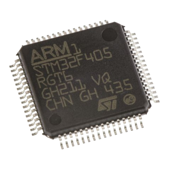
ST STM32F40 Series Reference Manual
Hide thumbs Also See for STM32F40 Series:
Table of Contents

Advertisement

Quick Links

STM32F40xxx, STM32F41xxx, STM32F42xxx, STM32F43xxx
Introduction
This reference manual targets application developers. It provides complete information on
how to use the STM32F405xx/07xx, STM32F415xx/17xx, STM32F42xxx and
STM32F43xxx microcontroller memory and peripherals.
The STM32F405xx/07xx, STM32F415xx/17xx, STM32F42xxx and STM32F43xxx constitute
a family of microcontrollers with different memory sizes, packages and peripherals.
For ordering information, mechanical and electrical device characteristics please refer to the
datasheets.
For information on the ARM Cortex™-M4F core, please refer to the Cortex™-M4F Technical
Reference Manual.
Related documents
Available from STMicroelectronics web site (http://www/st.com):
STM32F40x and STM32F41x datasheets
STM32F42x and STM32F43x databriefs
For information on the ARM Cortex™-M4 core with FPU, refer to the STM32F3xx/F4xxx
Cortex™-M4 programming manual (PM0214).
Table 1.
Microcontrollers
February 2013
Applicable products
Product family
Doc ID 018909 Rev 4
Reference manual
advanced ARM-based 32-bit MCUs
Part numbers and product categories
STM32F405xx, STM32F407xx, STM32F415xx, STM32F417xx,
STM32F427xx, STM32F437xx
RM0090
1/1422
www.st.com

Advertisement

Table of Contents
loading
Need help?

Need help?

Do you have a question about the STM32F40 Series and is the answer not in the manual?

Questions and answers

Summary of Contents for ST STM32F40 Series

  • Page 1: Table 1. Applicable Products

    For ordering information, mechanical and electrical device characteristics please refer to the datasheets. For information on the ARM Cortex™-M4F core, please refer to the Cortex™-M4F Technical Reference Manual. Related documents Available from STMicroelectronics web site (http://www/st.com): ■ STM32F40x and STM32F41x datasheets ■ STM32F42x and STM32F43x databriefs ■...
  • Page 2: Table Of Contents

    RM0090 Contents Contents Documentation conventions ....... . . 47 List of abbreviations for registers ....... 47 Glossary .
  • Page 3 Contents RM0090 3.5.3 Erase ........... 66 3.5.4 Programming .
  • Page 4 RM0090 Contents 5.1.3 Voltage regulator ......... . 92 Power supply supervisor .
  • Page 5 Contents RM0090 6.2.11 Internal/external clock measurement using TIM5/TIM11 ... 120 RCC registers ..........123 6.3.1 RCC clock control register (RCC_CR) .
  • Page 6 RM0090 Contents 6.3.25 RCC APB2 peripheral clock enabled in low power mode register for STM32F405xx/07xx and STM32F415xx/17xx for STM32F405xx/07xx and STM32F415xx/17xx(RCC_APB2LPENR) . . 171 6.3.26 RCC APB2 peripheral clock enabled in low power mode register for STM32F42xxx and STM32F43xxx (RCC_APB2LPENR) ..173 6.3.27 RCC Backup domain control register (RCC_BDCR) .
  • Page 7 Contents RM0090 7.4.4 GPIO port pull-up/pull-down register (GPIOx_PUPDR) (x = A..I/) ..........199 7.4.5 GPIO port input data register (GPIOx_IDR) (x = A..I) .
  • Page 8 RM0090 Contents 9.3.5 DMA streams ..........220 9.3.6 Source, destination and transfer modes .
  • Page 9 Contents RM0090 10.2.4 Functional description ........258 10.2.5 External interrupt/event line mapping .
  • Page 10 RM0090 Contents 11.9.3 Interleaved mode ......... 283 11.9.4 Alternate trigger mode .
  • Page 11 Contents RM0090 12.3.6 DAC trigger selection ........314 12.3.7 DMA request .
  • Page 12 RM0090 Contents 12.5.14 DAC status register (DAC_SR) ......328 12.5.15 DAC register map ........329 Digital camera interface (DCMI) .
  • Page 13 Contents RM0090 Advanced-control timers (TIM1&TIM8) ......353 14.1 TIM1&TIM8 introduction ........353 14.2 TIM1&TIM8 main features .
  • Page 14 RM0090 Contents 14.4.11 TIM1&TIM8 prescaler (TIMx_PSC) ......413 14.4.12 TIM1&TIM8 auto-reload register (TIMx_ARR) ....413 14.4.13 TIM1&TIM8 repetition counter register (TIMx_RCR) .
  • Page 15 Contents RM0090 15.4.5 TIMx status register (TIMx_SR) ......465 15.4.6 TIMx event generation register (TIMx_EGR) ....467 15.4.7 TIMx capture/compare mode register 1 (TIMx_CCMR1) .
  • Page 16 RM0090 Contents 16.5 TIM9 and TIM12 registers ........502 16.5.1 TIM9/12 control register 1 (TIMx_CR1) .
  • Page 17 Contents RM0090 17.3.4 Debug mode ..........530 17.4 TIM6&TIM7 registers .
  • Page 18 RM0090 Contents 19.6.4 WWDG register map ........547 Cryptographic processor (CRYP) .
  • Page 19 Contents RM0090 21.3.1 Operation ..........595 21.3.2 Error management .
  • Page 20 RM0090 Contents 23.3.1 Clock and prescalers ........627 23.3.2 Real-time clock and calendar .
  • Page 21 Contents RM0090 23.6.19 RTC alarm B sub second register (RTC_ALRMBSSR) ... . 661 23.6.20 RTC backup registers (RTC_BKPxR) ......662 23.6.21 RTC register map .
  • Page 22 RM0090 Contents Inter-integrated circuit (I C) interface ......708 25.1 C introduction ..........708 25.2 C main features .
  • Page 23 Contents RM0090 26.3.4 Fractional baud rate generation ......755 26.3.5 USART receiver tolerance to clock deviation ....764 26.3.6 Multiprocessor communication .
  • Page 24 RM0090 Contents 27.3.8 Disabling the SPI ......... 815 27.3.9 SPI communication using DMA (direct memory addressing) .
  • Page 25 Contents RM0090 28.4.3 Operating voltage range validation ......861 28.4.4 Card identification process ....... . . 862 28.4.5 Block write .
  • Page 26 RM0090 Contents 28.9.4 SDIO command register (SDIO_CMD) ......890 28.9.5 SDIO command response register (SDIO_RESPCMD) ... 891 28.9.6 SDIO response 1..4 register (SDIO_RESPx) .
  • Page 27 Contents RM0090 29.6 Ethernet functional description: DMA controller operation ... 944 29.6.1 Initialization of a transfer using DMA ......945 29.6.2 Host bus burst access .
  • Page 28 RM0090 Contents 30.6.1 SRP-capable host ........1032 30.6.2 USB host states .
  • Page 29 Contents RM0090 30.17.7 Worst case response time ....... . . 1151 30.17.8 OTG programming model .
  • Page 30 RM0090 Contents 31.12.1 CSR memory map ........1179 31.12.2 OTG_HS global registers .
  • Page 31 Contents RM0090 32.6.4 NAND Flash operations ........1361 32.6.5 NAND Flash pre-wait functionality .
  • Page 32 RM0090 Contents 33.13 DWT (data watchpoint trigger) ....... 1392 33.14 ITM (instrumentation trace macrocell) ......1392 33.14.1 General description .
  • Page 33 List of tables RM0090 List of tables Table 1. Applicable products ............1 Table 2.
  • Page 34 RM0090 List of tables Table 49. Analog watchdog channel selection ......... 269 Table 50.
  • Page 35 List of tables RM0090 Table 98. Interrupt control bits ........... . . 641 Table 99.
  • Page 36 RM0090 List of tables Table 140. AU_SIZE field ............874 Table 141.
  • Page 37 List of tables RM0090 Table 192. Nonmultiplexed I/Os PSRAM/SRAM ........1324 Table 193.
  • Page 38 RM0090 List of figures List of figures Figure 1. System architecture for STM32F405xx/07xx and STM32F415xx/17xx devices..50 Figure 2. System architecture for STM32F42xxx and STM32F43xxx devices ....50 Figure 3.
  • Page 39 List of figures RM0090 Figure 48. Alternate trigger: injected group of each ADC ....... . . 285 Figure 49.
  • Page 40 RM0090 List of figures Figure 98. Capture/compare channel 1 main circuit ........370 Figure 99.
  • Page 41 List of figures RM0090 Figure 150. Center-aligned PWM waveforms (ARR=8) ........444 Figure 151.
  • Page 42 RM0090 List of figures Figure 198. Independent watchdog block diagram ........537 Figure 199.
  • Page 43 List of figures RM0090 Figure 250. Start bit detection when oversampling by 16 or 8 ....... 750 Figure 251.
  • Page 44 RM0090 List of figures Figure 296. MSB Justified 24-bit frame length with CPOL = 0....... 825 Figure 297.
  • Page 45 List of figures RM0090 Figure 348. TxDMA operation in Default mode ......... . 949 Figure 349.
  • Page 46 RM0090 List of figures Figure 398. TRDT max timing case ..........1310 Figure 399.
  • Page 47: Documentation Conventions

    Documentation conventions RM0090 Documentation conventions The Cortex-M4 core with FPU will be referred to as Cortex-M4F throughout this document. List of abbreviations for registers The following abbreviations are used in register descriptions: read/write (rw) Software can read and write to these bits. read-only (r) Software can only read these bits.
  • Page 48: Glossary

    RM0090 Documentation conventions Glossary This section gives a brief definition of acronyms and abbreviations used in this document: ● The Cortex-M4 core with FPU will be referred to as Cortex-M4F throughout this document ● The CPU core integrates two debug ports: –...
  • Page 49: Memory And Bus Architecture

    Memory and bus architecture RM0090 Memory and bus architecture System architecture The main system consists of 32-bit multilayer AHB bus matrix that interconnects: ● Eight masters: – Cortex™-M4F core I-bus, D-bus and S-bus – DMA1 memory bus – DMA2 memory bus –...
  • Page 50: Figure 1. System Architecture For Stm32F405Xx/07Xx And Stm32F415Xx/17Xx Devices

    RM0090 Memory and bus architecture Figure 1. System architecture for STM32F405xx/07xx and STM32F415xx/17xx devices 64-Kbyte USB OTG Cortex-M4 DMA1 DMA2 Ethernet CCM data RAM ICODE Flash memory DCODE SRAM1 112 Kbyte SRAM2 16 Kbyte AHB1 APB1 peripherals AHB2 peripherals APB2 FSMC Static MemCtl Bus matrix-S...
  • Page 51: S0: I-Bus

    Memory and bus architecture RM0090 2.1.1 S0: I-bus This bus connects the Instruction bus of the Cortex™-M4F core to the BusMatrix. This bus is used by the core to fetch instructions. The target of this bus is a memory containing code (internal Flash memory/SRAM or external memories through the FSMC).
  • Page 52: Ahb/Apb Bridges (Apb)

    RM0090 Memory and bus architecture 2.1.9 AHB/APB bridges (APB) The two AHB/APB bridges, APB1 and APB2, provide full synchronous connections between the AHB and the two APB buses, allowing flexible selection of the peripheral frequency. Refer to the device datasheets for more details on APB1 and APB2 maximum frequencies, and to Table 2 on page 52 for the address mapping of AHB and APB peripherals.
  • Page 53 Memory and bus architecture RM0090 Table 2. STM32F4xx register boundary addresses (continued) Boundary address Peripheral Register map Section 31.12.6: OTG_HS register map on 0x4004 0000 - 0x4007 FFFF USB OTG HS page 1248 0x4002 9000 - 0x4002 93FF 0x4002 8C00 - 0x4002 8FFF Section 29.8.5: Ethernet register maps on 0x4002 8800 - 0x4002 8BFF ETHERNET MAC...
  • Page 54 RM0090 Memory and bus architecture Table 2. STM32F4xx register boundary addresses (continued) Boundary address Peripheral Register map 0x4001 3000 - 0x4001 33FF SPI1 Section 27.5.10: SPI register map on page 845 0x4001 2C00 - 0x4001 2FFF SDIO Section 28.9.16: SDIO register map on page 901 0x4001 2000 - 0x4001 23FF ADC1 - ADC2 - ADC3 Section 11.13.18: ADC register map on page 307...
  • Page 55: Embedded Sram

    Memory and bus architecture RM0090 2.3.1 Embedded SRAM The STM32F405xx/07xx and STM32F415xx/17xx feature 4 Kbytes of backup SRAM (see Section 5.1.2: Battery backup domain) plus 192 Kbytes of system SRAM. The STM32F42xxx and STM32F43xxx feature 4 Kbytes of backup SRAM (see Section 5.1.2: Battery backup domain) plus 256 Kbytes of system SRAM.
  • Page 56: Boot Configuration

    RM0090 Memory and bus architecture A mapping formula shows how to reference each word in the alias region to a corresponding bit in the bit-band region. The mapping formula is: bit_word_addr = bit_band_base + (byte_offset x 32) + (bit_number × 4) where: –...
  • Page 57: Table 4. Memory Mapping Vs. Boot Mode/Physical Remap

    CAN and USB OTG FS require an external clock (HSE) multiple of 1 MHz (ranging from 4 to 26 MHz). The embedded bootloader code is located in system memory. It is programmed by ST during production. For additional information, refer to application note AN2606.
  • Page 58 RM0090 Memory and bus architecture Table 4. Memory mapping vs. Boot mode/physical remap (continued) Boot/Remap in Boot/Remap in Boot/Remap in Addresses Remap in FSMC main Flash memory embedded SRAM System memory FSMC bank 1 0x0400 0000 - 0x07FF FFFF Reserved Reserved Reserved NOR/PSRAM 2...
  • Page 59: Embedded Flash Memory Interface

    Embedded Flash memory interface RM0090 Embedded Flash memory interface Introduction The Flash memory interface manages CPU AHB I-Code and D-Code accesses to the Flash memory. It implements the erase and program Flash memory operations and the read and write protection mechanisms. The Flash memory interface accelerates code execution with a system of instruction prefetch and cache lines.
  • Page 60: Embedded Flash Memory

    RM0090 Embedded Flash memory interface Embedded Flash memory The Flash memory has the following main features: ● Capacity up to 1 Mbyte for STM32F40x and STM32F41x and up to 2 Mbytes for STM32F42x and STM32F43x ● 128 bits wide data read ●...
  • Page 61: Read Interface

    Embedded Flash memory interface RM0090 Table 6. Flash memory organization (STM32F42x and STM32F43x) Block Name Block base addresses Size Sector 0 0x0800 0000 - 0x0800 3FFF 16 Kbyte Sector 1 0x0800 4000 - 0x0800 7FFF 16 Kbyte Sector 2 0x0800 8000 - 0x0800 BFFF 16 Kbyte Sector 3 0x0800 C000 - 0x0800 FFFF...
  • Page 62: Number Of Wait States According To Cpu Clock (Hclk) Frequency

    RM0090 Embedded Flash memory interface Note: On STM32F405xx/07xx and STM32F415xx/17xx devices: - when VOS = '0', the maximum value of f = 144 MHz. HCLK - when VOS = '1', the maximum value of f = 168 MHz. HCLK On STM32F42xxx and STM32F43xxx devices: - when VOS[1:0] = '0x01', the maximum value of f is 120 MHz.
  • Page 63: Adaptive Real-Time Memory Accelerator (Art Accelerator™)

    Embedded Flash memory interface RM0090 Decreasing the CPU frequency Modify the CPU clock source by writing the SW bits in the RCC_CFGR register If needed, modify the CPU clock prescaler by writing the HPRE bits in RCC_CFGR Check that the new CPU clock source or/and the new CPU clock prescaler value is/are taken into account by reading the clock source status (SWS bits) or/and the AHB prescaler value (HPRE bits), respectively, in the RCC_CFGR register Program the new number of wait states to the LATENCY bits in FLASH_ACR...
  • Page 64: Figure 4. Sequential 32-Bit Instruction Execution

    RM0090 Embedded Flash memory interface Figure 4. Sequential 32-bit instruction execution WAIT Without prefetch WAIT ins 1 ins 2 ins 3 ins 4 ins 5 ins 6 ins 7 ins 8 fetch fetch fetch fetch fetch fetch fetch fetch Read ins 1, 2, 3, 4 Gives ins 1, 2, 3, 4 Read ins 5, 6, 7, 8 Gives ins 5, 6, 7, 8 Wait data With prefetch...
  • Page 65: Erase And Program Operations

    Embedded Flash memory interface RM0090 Instruction cache memory To limit the time lost due to jumps, it is possible to retain 64 lines of 128 bits in an instruction cache memory. This feature can be enabled by setting the instruction cache enable (ICEN) bit in the FLASH_ACR register.
  • Page 66: Program/Erase Parallelism

    RM0090 Embedded Flash memory interface 3.5.2 Program/erase parallelism The Parallelism size is configured through the PSIZE field in the FLASH_CR register. It represents the number of bytes to be programmed each time a write operation occurs to the Flash memory. PSIZE is limited by the supply voltage and by whether the external V supply is used or not.
  • Page 67: Programming

    Embedded Flash memory interface RM0090 Mass Erase To perform Mass Erase, the following sequence is recommended: Check that no Flash memory operation is ongoing by checking the BSY bit in the FLASH_SR register Set the MER bit in the FLASH_CR register (on STM32F405xx/07xx and STM32F415xx/17xx devices) Set both the MER and MER1 bits in the FLASH_CR register (on STM32F42xxx and STM32F43xxx devices).
  • Page 68: Interrupts

    RM0090 Embedded Flash memory interface Programming and caches If a Flash memory write access concerns some data in the data cache, the Flash write access modifies the data in the Flash memory and the data in the cache. If an erase operation in Flash memory also concerns data in the data or instruction cache, you have to make sure that these data are rewritten before they are accessed during code execution.
  • Page 69: Table 11. Description Of The Option Bytes (Stm32F405Xx/07Xx And Stm32F415Xx/17Xx)

    Embedded Flash memory interface RM0090 Table 11. Description of the option bytes (STM32F405xx/07xx and STM32F415xx/17xx) Option bytes (word, address 0x1FFF C000) RDP: Read protection option byte. The read protection is used to protect the software code stored in Flash memory. 0xAA: Level 0, no protection Bits 15:8 0xCC: Level 2, chip protection (debug and boot from RAM features disabled)
  • Page 70: Table 12. Description Of The Option Bytes (Stm32F42Xxx And Stm32F43Xxx)

    RM0090 Embedded Flash memory interface Table 12. Description of the option bytes (STM32F42xxx and STM32F43xxx) Option bytes (word, address 0x1FFF C000) RDP: Read protection option byte. The read protection is used to protect the software code stored in Flash memory. 0xAA: Level 0, no protection Bit 15:8 0xCC: Level 2, chip protection (debug and boot from RAM features disabled)
  • Page 71: Programming User Option Bytes

    Embedded Flash memory interface RM0090 Table 12. Description of the option bytes (STM32F42xxx and STM32F43xxx) Option bytes (word, address 0x1FFE C008) Bit 15:12 0xF: not used nWRP: Flash memory write protection option bytes. Sectors 12 to 23 can be write protected. nWRPi: Bits 11: 0 0: Write protection active on sector i.
  • Page 72: Read Protection (Rdp)

    RM0090 Embedded Flash memory interface 3.6.3 Read protection (RDP) The user area in the Flash memory can be protected against read operations by an entrusted code. Three read protection levels are defined: ● Level 0: no read protection When the read protection level is set to Level 0 by writing 0xAA into the read protection option byte (RDP), all read/write operations (if no write protection is set) from/to the Flash memory or the backup SRAM are possible in all boot configurations (Flash user boot, debug or boot from RAM).
  • Page 73: Write Protections

    Embedded Flash memory interface RM0090 Table 13. Access versus read protection level Debug features, Boot from RAM or Booting from Flash memory Protection from System memory bootloader Memory area Level Read Write Erase Read Write Erase Level 1 Main Flash Memory and Backup SRAM Level 2 Level 1...
  • Page 74: One-Time Programmable Bytes

    RM0090 Embedded Flash memory interface sector cannot be erased or programmed. Consequently, a mass erase cannot be performed if one of the sectors is write-protected. If an erase/program operation to a write-protected part of the Flash memory is attempted (sector protected by write protection bit, OTP part locked or part of the Flash memory that can never be written like the ICP), the write protection error flag (WRPERR) is set in the FLASH_SR register.
  • Page 75: Flash Interface Registers

    Embedded Flash memory interface RM0090 Table 14. OTP area organization (continued) Block [128:96] [95:64] [63:32] [31:0] Address byte 0 OTP15 OTP15 OTP15 OTP15 0x1FFF 79E0 OTP15 OTP15 OTP15 OTP15 0x1FFF 79F0 LOCKB15 ... LOCKB11 ... LOCKB7 ... LOCKB3 ... Lock block 0x1FFF 7A00 LOCKB12 LOCKB8...
  • Page 76 RM0090 Embedded Flash memory interface Bit 8 PRFTEN: Prefetch enable 0: Prefetch is disabled 1: Prefetch is enabled Bits 7:3 Reserved, must be kept cleared. Bits 2:0 LATENCY: Latency These bits represent the ratio of the CPU clock period to the Flash memory access time. 000: Zero wait state 001: One wait state 010: Two wait states...
  • Page 77: Flash Key Register (Flash_Keyr)

    Embedded Flash memory interface RM0090 3.8.2 Flash key register (FLASH_KEYR) The Flash key register is used to allow access to the Flash control register and so, to allow program and erase operations. Address offset: 0x04 Reset value: 0x0000 0000 Access: no wait state, word access KEY[31:16] KEY[15:0] Bits 31:0 FKEYR: FPEC key...
  • Page 78: Flash Status Register (Flash_Sr)

    RM0090 Embedded Flash memory interface 3.8.4 Flash status register (FLASH_SR) The Flash status register gives information on ongoing program and erase operations. Address offset: 0x0C Reset value: 0x0000 0000 Access: no wait state, word, half-word and byte access Reserved PGSERR PGPERR PGAERR WRPERR OPERR Reserved Reserved...
  • Page 79: Flash Control Register (Flash_Cr) For

    Embedded Flash memory interface RM0090 Bits 3:2 Reserved, must be kept cleared. Bit 1 OPERR: Operation error Set by hardware when a flash operation (programming / erase /read) request is detected and can not be run because of parallelism, alignment, or write protection error. This bit is set only if error interrupts are enabled (ERRIE = 1).
  • Page 80: Stm32F42Xxx And Stm32F43Xxx

    RM0090 Embedded Flash memory interface Bits 15:10 Reserved, must be kept cleared. Bits 9:8 PSIZE: Program size These bits select the program parallelism. 00 program x8 01 program x16 10 program x32 11 program x64 Bits 6:3 SNB: Sector number These bits select the sector to erase.
  • Page 81 Embedded Flash memory interface RM0090 Bit 31 LOCK: Lock Write to 1 only. When it is set, this bit indicates that the FLASH_CR register is locked. It is cleared by hardware after detecting the unlock sequence. In the event of an unsuccessful unlock operation, this bit remains set until the next reset. Bits 31:26 Reserved, must be kept cleared.
  • Page 82: Flash Option Control Register (Flash_Optcr)

    RM0090 Embedded Flash memory interface Bit 2 MER: Mass Erase of bank 1 sectors Erase activated of bank 1 sectors. Bit 1 SER: Sector Erase Sector Erase activated. Bit 0 PG: Programming Flash programming activated. 3.8.7 Flash option control register (FLASH_OPTCR) The FLASH_OPTCR register is used to modify the user option bytes.
  • Page 83: Flash Option Control Register (Flash_Optcr1)

    Embedded Flash memory interface RM0090 Bits 3:2 BOR_LEV: BOR reset Level These bits contain the supply level threshold that activates/releases the reset. They can be written to program a new BOR level. By default, BOR is off. When the supply voltage (V drops below the selected BOR level, a device reset is generated.
  • Page 84: Flash Interface Register Map

    RM0090 Embedded Flash memory interface 3.8.9 Flash interface register map Table 15. Flash register map and reset values (STM32F405xx/07xx and STM32F415xx/17xx) Offset Register FLASH_ACR LATENCY 0x00 Reserved Reserved Reset value FLASH_KEY KEY[31:16] KEY[15:0] 0x04 Reset value FLASH_OPT OPTKEYR[31:16] OPTKEYR[15:0] KEYR 0x08 Reset value FLASH_SR...
  • Page 85 Embedded Flash memory interface RM0090 Table 16. Flash register map and reset values (STM32F42xxx and STM32F43xxx) (continued) Offset Register FLASH_OPTCR nWRP[11:0] RDP[7:0] 0x14 Reset value 1 0 1 FLASH_ nWRP[11:0] OPTCR1 0x18 Reserved Reset value 85/1422 Doc ID 018909 Rev 4...
  • Page 86: Crc Calculation Unit

    RM0090 CRC calculation unit CRC calculation unit This section applies to the whole STM32F4xx family, unless otherwise specified. CRC introduction The CRC (cyclic redundancy check) calculation unit is used to get a CRC code from a 32-bit data word and a fixed generator polynomial. Among other applications, CRC-based techniques are used to verify data transmission or storage integrity.
  • Page 87: Crc Registers

    CRC calculation unit RM0090 Each write operation into the data register creates a combination of the previous CRC value and the new one (CRC computation is done on the whole 32-bit data word, and not byte per byte). The write operation is stalled until the end of the CRC computation, thus allowing back-to- back write accesses or consecutive write and read accesses.
  • Page 88: Control Register (Crc_Cr)

    RM0090 CRC calculation unit Bits 7:0 General-purpose 8-bit data register bits Can be used as a temporary storage location for one byte. This register is not affected by CRC resets generated by the RESET bit in the CRC_CR register. 4.4.3 Control register (CRC_CR) Address offset: 0x08 Reset value: 0x0000 0000...
  • Page 89: Power Controller (Pwr)

    Power controller (PWR) RM0090 Power controller (PWR) This section applies to the whole STM32F4xx family, unless otherwise specified. Power supplies The device requires a 1.8-to-3.6 V operating voltage supply (V ). An embedded linear voltage regulator is used to supply the internal 1.2 V digital power. The real-time clock (RTC), the RTC backup registers, and the backup SRAM (BKP SRAM) can be powered from the V voltage when the main V...
  • Page 90: Independent A/D Converter Supply And Reference Voltage

    RM0090 Power controller (PWR) 5.1.1 Independent A/D converter supply and reference voltage To improve conversion accuracy, the ADC has an independent power supply which can be separately filtered and shielded from noise on the PCB. ● The ADC voltage supply input is available on a separate V pin.
  • Page 91 Power controller (PWR) RM0090 Note: Due to the fact that the switch only sinks a limited amount of current (3 mA), the use of GPIOs PI8 and PC13 to PC15 are restricted: only one I/O at a time can be used as an output, the speed has to be limited to 2 MHz with a maximum load of 30 pF and these I/Os must not be used as a current source (e.g.
  • Page 92: Voltage Regulator

    RM0090 Power controller (PWR) When the backup domain is supplied by V (analog switch connected to V ), the backup SRAM is powered from V which replaces the V power supply to save battery life. When the backup domain is supplied by V (analog switch connected to V because is not present), the backup SRAM is powered by a dedicated low power regulator.
  • Page 93 Power controller (PWR) RM0090 When activated by software, the voltage regulator is always enabled after Reset. It works in three different modes depending on the application modes. ● In Run mode, the regulator supplies full power to the 1.2 V domain (core, memories and digital peripherals).
  • Page 94: Power Supply Supervisor

    RM0090 Power controller (PWR) Power supply supervisor 5.2.1 Power-on reset (POR)/power-down reset (PDR) The device has an integrated POR/PDR circuitry that allows proper operation starting from to 1.8 V. The device remains in Reset mode when V is below a specified threshold, , without the need for an external reset circuit.
  • Page 95: Programmable Voltage Detector (Pvd)

    Power controller (PWR) RM0090 The BOR threshold hysteresis is ~100 mV (between the rising and the falling edge of the supply voltage). Figure 10. BOR thresholds VDD/VDDA 100 mV BOR threshold hysteresis Reset MS30432V1 5.2.3 Programmable voltage detector (PVD) You can use the PVD to monitor the V power supply by comparing it to a threshold selected by the PLS[2:0] bits in the PWR power control register (PWR_CR) for...
  • Page 96: Low-Power Modes

    RM0090 Power controller (PWR) Figure 11. PVD thresholds 100 mV PVD threshold hysteresis PVD output MS30433V2 Low-power modes By default, the microcontroller is in Run mode after a system or a power-on reset. In Run mode the CPU is clocked by HCLK and the program code is executed. Several low-power modes are available to save power when the CPU does not need to be kept running, for example when waiting for an external event.
  • Page 97: Slowing Down System Clocks

    Power controller (PWR) RM0090 Table 18. Low-power mode summary Effect on Effect on 1.2 V Mode name Entry Wakeup Voltage regulator domain clocks domain clocks Any interrupt CPU CLK OFF Sleep no effect on other (Sleep now or None clocks or analog Wakeup event Sleep-on-exit) clock sources...
  • Page 98: Sleep Mode

    RM0090 Power controller (PWR) Disabling the peripherals clocks in Sleep mode can be performed automatically by resetting the corresponding bit in RCC_AHBxLPENR and RCC_APBxLPENR registers. 5.3.3 Sleep mode Entering Sleep mode The Sleep mode is entered by executing the WFI (Wait For Interrupt) or WFE (Wait for Event) instructions.
  • Page 99: Stop Mode

    Power controller (PWR) RM0090 Table 20. Sleep-on-exit entry and exit Sleep-on-exit Description WFI (wait for interrupt) while: – SLEEPDEEP = 0 and Mode entry – SLEEPONEXIT = 1 Refer to the Cortex™-M4F System Control register. Interrupt: refer to Table 45: Vector table for STM32F405xx/07xx and Mode exit STM32F415xx/17xx Table 46: Vector table for STM32F42xxx and...
  • Page 100: Table 21. Stop Operating Modes

    RM0090 Power controller (PWR) If Flash memory programming is ongoing, the Stop mode entry is delayed until the memory access is finished. If an access to the APB domain is ongoing, The Stop mode entry is delayed until the APB access is finished.
  • Page 101: Standby Mode

    Power controller (PWR) RM0090 5.3.5 Standby mode The Standby mode allows to achieve the lowest power consumption. It is based on the Cortex™-M4F deepsleep mode, with the voltage regulator disabled. The 1.2 V domain is consequently powered off. The PLLs, the HSI oscillator and the HSE oscillator are also switched off.
  • Page 102: Programming The Rtc Alternate Functions To Wake Up The Device From The Stop And Standby Modes

    RM0090 Power controller (PWR) I/O states in Standby mode In Standby mode, all I/O pins are high impedance except for: ● Reset pad (still available) ● RTC_AF1 pin (PC13) if configured for tamper, time stamp, RTC Alarm out, or RTC clock calibration out ●...
  • Page 103 Power controller (PWR) RM0090 RTC alternate functions to wake up the device from the Stop mode ● To wake up the device from the Stop mode with an RTC alarm event, it is necessary to: Configure the EXTI Line 17 to be sensitive to rising edges (Interrupt or Event modes) Enable the RTC Alarm Interrupt in the RTC_CR register Configure the RTC to generate the RTC alarm...
  • Page 104 RM0090 Power controller (PWR) Safe RTC alternate function wakeup flag clearing sequence If the selected RTC alternate function is set before the PWR wakeup flag (WUTF) is cleared, it will not be detected on the next event as detection is made once on the rising edge. To avoid bouncing on the pins onto which the RTC alternate functions are mapped, and exit correctly from the Stop and Standby modes, it is recommended to follow the sequence below before entering the Standby mode:...
  • Page 105: Power Control Registers

    Power controller (PWR) RM0090 Power control registers 5.4.1 PWR power control register (PWR_CR) STM32F405xx/07xx and STM32F415xx/17xx Address offset: 0x00 Reset value: 0x0000 4000 (reset by wakeup from Standby mode) Reserved FPDS PLS[2:0] PVDE CSBF CWUF PDDS LPDS Res. Reserved rc_w1 rc_w1 Bits 31:15 Reserved, must be kept at reset value.
  • Page 106: Pwr Power Control Register (Pwr_Cr)

    RM0090 Power controller (PWR) Bit 4 PVDE: Power voltage detector enable This bit is set and cleared by software. 0: PVD disabled 1: PVD enabled Bit 3 CSBF: Clear standby flag This bit is always read as 0. 0: No effect 1: Clear the SBF Standby Flag (write).
  • Page 107 Power controller (PWR) RM0090 Bits 31:16 Reserved, must be kept at reset value. Bits15:14 VOS[1:0]: Regulator voltage scaling output selection These bits control the main internal voltage regulator output voltage to achieve a trade-off between performance and power consumption when the device does not operate at the maximum frequency (refer to the STM32F42xx and STM32F43xx datasheets for more details).
  • Page 108: Pwr Power Control/Status Register (Pwr_Csr)

    RM0090 Power controller (PWR) Bit 3 CSBF: Clear standby flag This bit is always read as 0. 0: No effect 1: Clear the SBF Standby Flag (write). Bit 2 CWUF: Clear wakeup flag This bit is always read as 0. 0: No effect 1: Clear the WUF Wakeup Flag after 2 System clock cycles Bit 1 PDDS: Power-down deepsleep...
  • Page 109: Pwr Register Map

    Power controller (PWR) RM0090 Bit 8 EWUP: Enable WKUP pin This bit is set and cleared by software. 0: WKUP pin is used for general purpose I/O. An event on the WKUP pin does not wakeup the device from Standby mode. 1: WKUP pin is used for wakeup from Standby mode and forced in input pull down configuration (rising edge on WKUP pin wakes-up the system from Standby mode).
  • Page 110: Table 25. Pwr - Register Map And Reset Values For Stm32F42Xxx And Stm32F43Xxx

    RM0090 Power controller (PWR) Table 25. PWR - register map and reset values for STM32F42xxx and STM32F43xxx Offset Register PWR_CR PLS[2:0] 0x000 Reserved Reserved Reset value PWR_CSR 0x004 Reserved Reserved Reserved Reset value Refer to Table 2 on page 52 for the register boundary addresses.
  • Page 111: Reset And Clock Control For (Rcc)

    Reset and clock control for (RCC) RM0090 Reset and clock control for (RCC) Reset There are three types of reset, defined as system Reset, power Reset and backup domain Reset. 6.1.1 System reset A system reset sets all registers to their reset values except the reset flags in the clock controller CSR register and the registers in the Backup domain (see Figure A system reset is generated when one of the following events occurs:...
  • Page 112: Power Reset

    In this case, whenever a Stop mode entry sequence is successfully executed, the device is reset instead of entering the Stop mode. For further information on the user option bytes, refer to the STM32F40x and STM32F41x Flash programming manual available from your ST sales office. 6.1.2 Power reset...
  • Page 113: Backup Domain Reset

    Reset and clock control for (RCC) RM0090 6.1.3 Backup domain reset The backup domain reset sets all RTC registers and the RCC_BDCR register to their reset values. The BKPSRAM is not affected by this reset. The only way of resetting the BKPSRAM is through the Flash interface by requesting a protection level change from 1 to A backup domain reset is generated when one of the following events occurs: Software reset, triggered by setting the BDRST bit in the...
  • Page 114: Figure 13. Clock Tree

    RM0090 Reset and clock control for (RCC) Figure 13. Clock tree Watchdog IWDGCLK enable to independent LSI RC watchdog 32 kHz RTCSEL[1:0] RTCCLK OSC32_IN enable to RTC LSE OS C 32.768 kHz OSC32_OUT SYSCLK MCO2 /1 to 5 HSE_RTC MCO1 /1 to 5 Peripheral Ethernet...
  • Page 115 Reset and clock control for (RCC) RM0090 The clock controller provides a high degree of flexibility to the application in the choice of the external crystal or the oscillator to run the core and peripherals at the highest frequency and, guarantee the appropriate frequency for peripherals that need a specific clock like Ethernet, USB OTG FS and HS, I2S and SDIO.
  • Page 116: Hse Clock

    RM0090 Reset and clock control for (RCC) 6.2.1 HSE clock The high speed external clock signal (HSE) can be generated from two possible clock sources: ● HSE external crystal/ceramic resonator ● HSE external user clock The resonator and the load capacitors have to be placed as close as possible to the oscillator pins in order to minimize output distortion and startup stabilization time.
  • Page 117: Hsi Clock

    Calibration RC oscillator frequencies can vary from one chip to another due to manufacturing process variations, this is why each device is factory calibrated by ST for 1% accuracy at T = 25 °C. After reset, the factory calibration value is loaded in the HSICAL[7:0] bits in the...
  • Page 118: Lse Clock

    RM0090 Reset and clock control for (RCC) 6.2.4 LSE clock The LSE crystal is a 32.768 kHz low-speed external (LSE) crystal or ceramic resonator. It has the advantage providing a low-power but highly accurate clock source to the real-time clock peripheral (RTC) for clock/calendar or other timing functions. The LSE crystal is switched on and off using the LSEON bit in RCC Backup domain control register...
  • Page 119: Rtc/Awu Clock

    Reset and clock control for (RCC) RM0090 CSSI), allowing the MCU to perform rescue operations. The CSSI is linked to the Cortex™- M4F NMI (non-maskable interrupt) exception vector. Note: When the CSS is enabled, if the HSE clock happens to fail, the CSS generates an interrupt, which causes the automatic generation of an NMI.
  • Page 120: Watchdog Clock

    RM0090 Reset and clock control for (RCC) 6.2.9 Watchdog clock If the independent watchdog (IWDG) is started by either hardware option or software access, the LSI oscillator is forced ON and cannot be disabled. After the LSI oscillator temporization, the clock is provided to the IWDG. 6.2.10 Clock-out capability Two microcontroller clock output (MCO) pins are available:...
  • Page 121: Figure 15. Frequency Measurement With Tim5 In Input Capture Mode

    Reset and clock control for (RCC) RM0090 with the same resolution, and trim the source to compensate for manufacturing-process and/or temperature- and voltage-related frequency deviations. The HSI oscillator has dedicated, user-accessible calibration bits for this purpose. The basic concept consists in providing a relative measurement (e.g. HSI/LSE ratio): the precision is therefore tightly linked to the ratio between the two clock sources.
  • Page 122: Figure 16. Frequency Measurement With Tim11 In Input Capture Mode

    RM0090 Reset and clock control for (RCC) Figure 16. Frequency measurement with TIM11 in Input capture mode TIM11 TI1_RMP[1:0] GPIO HSE_RTC(1 MHz) ai18433 Doc ID 018909 Rev 4 122/1422...
  • Page 123: Rcc Registers

    Reset and clock control for (RCC) RM0090 RCC registers Refer to Section 1.1: List of abbreviations for registers for a list of abbreviations used in register descriptions. 6.3.1 RCC clock control register (RCC_CR) Address offset: 0x00 Reset value: 0x0000 XX83 where X is undefined. Access: no wait state, word, half-word and byte access PLLI2S PLLI2S...
  • Page 124 RM0090 Reset and clock control for (RCC) Bit 18 HSEBYP: HSE clock bypass Set and cleared by software to bypass the oscillator with an external clock. The external clock must be enabled with the HSEON bit, to be used by the device. The HSEBYP bit can be written only if the HSE oscillator is disabled.
  • Page 125: Rcc Pll Configuration Register (Rcc_Pllcfgr)

    Reset and clock control for (RCC) RM0090 6.3.2 RCC PLL configuration register (RCC_PLLCFGR) Address offset: 0x04 Reset value: 0x2400 3010 Access: no wait state, word, half-word and byte access. This register is used to configure the PLL clock outputs according to the formulas: ●...
  • Page 126 RM0090 Reset and clock control for (RCC) Bits 17:16 PLLP: Main PLL (PLL) division factor for main system clock Set and cleared by software to control the frequency of the general PLL output clock. These bits can be written only if PLL is disabled. Caution: The software has to set these bits correctly not to exceed 168 MHz on this domain.
  • Page 127: Rcc Clock Configuration Register (Rcc_Cfgr)

    Reset and clock control for (RCC) RM0090 6.3.3 RCC clock configuration register (RCC_CFGR) Address offset: 0x08 Reset value: 0x0000 0000 Access: 0 ≤ wait state ≤ 2, word, half-word and byte access 1 or 2 wait states inserted only if the access occurs during a clock source switch. I2SSC MCO2 MCO2 PRE[2:0]...
  • Page 128 RM0090 Reset and clock control for (RCC) Bits 22:21 MCO1: Microcontroller clock output 1 Set and cleared by software. Clock source selection may generate glitches on MCO1. It is highly recommended to configure these bits only after reset before enabling the external oscillators and PLL.
  • Page 129: Rcc Clock Interrupt Register (Rcc_Cir)

    Reset and clock control for (RCC) RM0090 Bits 7:4 HPRE: AHB prescaler Set and cleared by software to control AHB clock division factor. Caution: The clocks are divided with the new prescaler factor from 1 to 16 AHB cycles after HPRE write.
  • Page 130 RM0090 Reset and clock control for (RCC) Bits 31:24 Reserved, must be kept at reset value. Bit 23 CSSC: Clock security system interrupt clear This bit is set by software to clear the CSSF flag. 0: No effect 1: Clear CSSF flag Bits 22 Reserved, must be kept at reset value.
  • Page 131 Reset and clock control for (RCC) RM0090 Bit 10 HSIRDYIE: HSI ready interrupt enable Set and cleared by software to enable/disable interrupt caused by the HSI oscillator stabilization. 0: HSI ready interrupt disabled 1: HSI ready interrupt enabled Bit 9 LSERDYIE: LSE ready interrupt enable Set and cleared by software to enable/disable interrupt caused by the LSE oscillator stabilization.
  • Page 132: Rcc Ahb1 Peripheral Reset Register (Rcc_Ahb1Rstr)

    RM0090 Reset and clock control for (RCC) Bit 0 LSIRDYF: LSI ready interrupt flag Set by hardware when the internal low speed clock becomes stable and LSIRDYDIE is set. Cleared by software setting the LSIRDYC bit. 0: No clock ready interrupt caused by the LSI oscillator 1: Clock ready interrupt caused by the LSI oscillator 6.3.5 RCC AHB1 peripheral reset register (RCC_AHB1RSTR)
  • Page 133 Reset and clock control for (RCC) RM0090 Bit 8 GPIOIRST: IO port I reset Set and cleared by software. 0: does not reset IO port I 1: resets IO port I Bit 7 GPIOHRST: IO port H reset Set and cleared by software. 0: does not reset IO port H 1: resets IO port H Bits 6 GPIOGRST: IO port G reset...
  • Page 134: Rcc Ahb2 Peripheral Reset Register (Rcc_Ahb2Rstr)

    RM0090 Reset and clock control for (RCC) 6.3.6 RCC AHB2 peripheral reset register (RCC_AHB2RSTR) Address offset: 0x14 Reset value: 0x0000 0000 Access: no wait state, word, half-word and byte access Reserved OTGFS HASH CRYP DCMI Reserved Reserved Bits 31:8 Reserved, must be kept at reset value. Bit 7 OTGFSRST: USB OTG FS module reset Set and cleared by software.
  • Page 135: Rcc Ahb3 Peripheral Reset Register (Rcc_Ahb3Rstr)

    Reset and clock control for (RCC) RM0090 6.3.7 RCC AHB3 peripheral reset register (RCC_AHB3RSTR) Address offset: 0x18 Reset value: 0x0000 0000 Access: no wait state, word, half-word and byte access. Reserved FSMCRST Reserved Bits 31:1 Reserved, must be kept at reset value. Bit 0 FSMCRST: Flexible static memory controller module reset Set and cleared by software.
  • Page 136 RM0090 Reset and clock control for (RCC) Bit 27 Reserved, must be kept at reset value. Bit 26 CAN2RST: CAN2 reset Set and cleared by software. 0: does not reset CAN2 1: resets CAN2 Bit 25 CAN1RST: CAN1 reset Set and cleared by software. 0: does not reset CAN1 1: resets CAN1 Bit 24 Reserved, must be kept at reset value.
  • Page 137 Reset and clock control for (RCC) RM0090 Bit 14 SPI2RST: SPI2 reset Set and cleared by software. 0: does not reset SPI2 1: resets SPI2 Bits 13:12 Reserved, must be kept at reset value. Bit 11 WWDGRST: Window watchdog reset Set and cleared by software.
  • Page 138: Rcc Apb1 Peripheral Reset Register For

    RM0090 Reset and clock control for (RCC) 6.3.9 RCC APB1 peripheral reset register for STM32F42xxx and STM32F43xxx (RCC_APB1RSTR) Address offset: 0x20 Reset value: 0x0000 0000 Access: no wait state, word, half-word and byte access. UART8R UART7R CAN2 CAN1 I2C3 I2C2 I2C1 UART5 UART4...
  • Page 139 Reset and clock control for (RCC) RM0090 Bit 22 I2C2RST: I2C2 reset Set and cleared by software. 0: does not reset I2C2 1: resets I2C2 Bit 21 I2C1RST: I2C1 reset Set and cleared by software. 0: does not reset I2C1 1: resets I2C1 Bit 20 UART5RST: UART5 reset Set and cleared by software.
  • Page 140 RM0090 Reset and clock control for (RCC) Bit 7 TIM13RST: TIM13 reset Set and cleared by software. 0: does not reset TIM13 1: resets TIM13 Bit 6 TIM12RST: TIM12 reset Set and cleared by software. 0: does not reset TIM12 1: resets TIM12 Bit 5 TIM7RST: TIM7 reset Set and cleared by software.
  • Page 141: For Stm32F405Xx/07Xx And Stm32F415Xx/17Xx

    Reset and clock control for (RCC) RM0090 6.3.10 RCC APB2 peripheral reset register (RCC_APB2RSTR) for STM32F405xx/07xx and STM32F415xx/17xx Address offset: 0x24 Reset value: 0x0000 0000 Access: no wait state, word, half-word and byte access. TIM11 TIM10 TIM9 Reserved SPI1 SDIO USART6 USART1 TIM8...
  • Page 142 RM0090 Reset and clock control for (RCC) Bit 8 ADCRST: ADC interface reset (common to all ADCs) Set and cleared by software. 0: does not reset the ADC interface 1: resets the ADC interface Bits 7:6 Reserved, must be kept at reset value. Bit 5 USART6RST: USART6 reset Set and cleared by software.
  • Page 143: Rcc Apb2 Peripheral Reset Register For Stm32F42Xxx And Stm32F43Xxx (Rcc_Apb2Rstr)

    Reset and clock control for (RCC) RM0090 6.3.11 RCC APB2 peripheral reset register for STM32F42xxx and STM32F43xxx (RCC_APB2RSTR) Address offset: 0x24 Reset value: 0x0000 0000 Access: no wait state, word, half-word and byte access. TIM11 TIM10 TIM9 SPI6 SPI5 Reserved Res.
  • Page 144 RM0090 Reset and clock control for (RCC) Bit 12 SPI1RST: SPI1 reset Set and cleared by software. 0: does not reset SPI1 1: resets SPI1 Bit 11 SDIORST: SDIO reset Set and cleared by software. 0: does not reset the SDIO module 1: resets the SDIO module Bits 10:9 Reserved, must be kept at reset value.
  • Page 145: Rcc Ahb1 Peripheral Clock Enable Register (Rcc_Ahb1Enr)

    Reset and clock control for (RCC) RM0090 6.3.12 RCC AHB1 peripheral clock enable register (RCC_AHB1ENR) Address offset: 0x30 Reset value: 0x0010 0000 Access: no wait state, word, half-word and byte access. ETHMA OTGHS OTGHS ETHMA ETHMA ETHMA CCMDATA BKPSR CPTPE DMA2EN DMA1EN Res.
  • Page 146 RM0090 Reset and clock control for (RCC) Bit 21 DMA1EN: DMA1 clock enable Set and cleared by software. 0: DMA1 clock disabled 1: DMA1 clock enabled Bit 20 CCMDATARAMEN: CCM data RAM clock enable Set and cleared by software. 0: CCM data RAM clock disabled 1: CCM data RAM clock enabled Bits 19 Reserved, must be kept at reset value.
  • Page 147: Rcc Ahb2 Peripheral Clock Enable Register (Rcc_Ahb2Enr)

    Reset and clock control for (RCC) RM0090 Bit 2 GPIOCEN: IO port C clock enable Set and cleared by software. 0: IO port C clock disabled 1: IO port C clock enabled Bit 1 GPIOBEN: IO port B clock enable Set and cleared by software.
  • Page 148: Rcc Ahb3 Peripheral Clock Enable Register (Rcc_Ahb3Enr)

    RM0090 Reset and clock control for (RCC) Bit 4 CRYPEN: Cryptographic modules clock enable Set and cleared by software. 0: cryptographic module clock disabled 1: cryptographic module clock enabled Bit 3:1 Reserved, must be kept at reset value. Bit 0 DCMIEN: Camera interface enable Set and cleared by software.
  • Page 149 Reset and clock control for (RCC) RM0090 Bits 31:30 Reserved, must be kept at reset value. Bit 29 DACEN: DAC interface clock enable Set and cleared by software. 0: DAC interface clock disabled 1: DAC interface clock enable Bit 28 PWREN: Power interface clock enable Set and cleared by software.
  • Page 150 RM0090 Reset and clock control for (RCC) Bit 17 USART2EN: USART2 clock enable Set and cleared by software. 0: USART2 clock disabled 1: USART2 clock enabled Bit 16 Reserved, must be kept at reset value. Bit 15 SPI3EN: SPI3 clock enable Set and cleared by software.
  • Page 151: Rcc Apb1 Peripheral Clock Enable Register For Stm32F42Xxx And Stm32F43Xxx(Rcc_Apb1Enr)

    Reset and clock control for (RCC) RM0090 Bit 2 TIM4EN: TIM4 clock enable Set and cleared by software. 0: TIM4 clock disabled 1: TIM4 clock enabled Bit 1 TIM3EN: TIM3 clock enable Set and cleared by software. 0: TIM3 clock disabled 1: TIM3 clock enabled Bit 0 TIM2EN: TIM2 clock enable Set and cleared by software.
  • Page 152 RM0090 Reset and clock control for (RCC) Bit 26 CAN2EN: CAN 2 clock enable Set and cleared by software. 0: CAN 2 clock disabled 1: CAN 2 clock enabled Bit 25 CAN1EN: CAN 1 clock enable Set and cleared by software. 0: CAN 1 clock disabled 1: CAN 1 clock enabled Bit 24 Reserved, must be kept at reset value.
  • Page 153 Reset and clock control for (RCC) RM0090 Bits 13:12 Reserved, must be kept at reset value. Bit 11 WWDGEN: Window watchdog clock enable Set and cleared by software. 0: Window watchdog clock disabled 1: Window watchdog clock enabled Bit 10:9 Reserved, must be kept at reset value. Bit 8 TIM14EN: TIM14 clock enable Set and cleared by software.
  • Page 154: Rcc Apb2 Peripheral Clock Enable Register (Rcc_Apb2Enr)

    RM0090 Reset and clock control for (RCC) 6.3.17 RCC APB2 peripheral clock enable register (RCC_APB2ENR) for STM32F405xx/07xx and STM32F415xx/17xx Address offset: 0x44 Reset value: 0x0000 0000 Access: no wait state, word, half-word and byte access. TIM11 TIM10 TIM9 Reserved SPI1 SDIO ADC3 ADC2...
  • Page 155 Reset and clock control for (RCC) RM0090 Bit 9 ADC2EN: ADC2 clock enable Set and cleared by software. 0: ADC2 clock disabled 1: ADC2 clock disabled Bit 8 ADC1EN: ADC1 clock enable Set and cleared by software. 0: ADC1 clock disabled 1: ADC1 clock disabled Bits 7:6 Reserved, must be kept at reset value.
  • Page 156: Rcc Apb2 Peripheral Clock Enable Register For Stm32F42Xxx And Stm32F43Xxx(Rcc_Apb2Enr)

    RM0090 Reset and clock control for (RCC) 6.3.18 RCC APB2 peripheral clock enable register for STM32F42xxx and STM32F43xxx(RCC_APB2ENR) Address offset: 0x44 Reset value: 0x0000 0000 Access: no wait state, word, half-word and byte access. TIM11 TIM10 TIM9 SPI6EN SPI5EN Reserved Res.
  • Page 157 Reset and clock control for (RCC) RM0090 Bit 12 SPI1EN: SPI1 clock enable Set and cleared by software. 0: SPI1 clock disabled 1: SPI1 clock enabled Bit 11 SDIOEN: SDIO clock enable Set and cleared by software. 0: SDIO module clock disabled 1: SDIO module clock enabled Bit 10 ADC3EN: ADC3 clock enable Set and cleared by software.
  • Page 158: Rcc Ahb1 Peripheral Clock Enable In Low Power Mode Register For Stm32F405Xx/07Xx And Stm32F415Xx/17Xx (Rcc_Ahb1Lpenr)

    RM0090 Reset and clock control for (RCC) 6.3.19 RCC AHB1 peripheral clock enable in low power mode register for STM32F405xx/07xx and STM32F415xx/17xx (RCC_AHB1LPENR) Address offset: 0x50 Reset value: 0x7E67 91FF Access: no wait state, word, half-word and byte access. BKPSRA OTGHS OTGHS ETHPTP...
  • Page 159 Reset and clock control for (RCC) RM0090 Bit 21 DMA1LPEN: DMA1 clock enable during Sleep mode Set and cleared by software. 0: DMA1 clock disabled during Sleep mode 1: DMA1 clock enabled during Sleep mode Bits 20:19 Reserved, must be kept at reset value. Bit 18 BKPSRAMLPEN: Backup SRAM interface clock enable during Sleep mode Set and cleared by software.
  • Page 160 RM0090 Reset and clock control for (RCC) Bit 4 GPIOELPEN: IO port E clock enable during Sleep mode Set and cleared by software. 0: IO port E clock disabled during Sleep mode 1: IO port E clock enabled during Sleep mode Bit 3 GPIODLPEN: IO port D clock enable during Sleep mode Set and cleared by software.
  • Page 161: Rcc Ahb1 Peripheral Clock Enable In Low Power Mode Register For Stm32F42Xxx And Stm32F43Xxx (Rcc_Ahb1Lpenr)

    Reset and clock control for (RCC) RM0090 6.3.20 RCC AHB1 peripheral clock enable in low power mode register for STM32F42xxx and STM32F43xxx (RCC_AHB1LPENR) Address offset: 0x50 Reset value: 0x7E67 91FF Access: no wait state, word, half-word and byte access. BKPSRA OTGHS OTGHS ETHPTP...
  • Page 162 RM0090 Reset and clock control for (RCC) Bit 21 DMA1LPEN: DMA1 clock enable during Sleep mode Set and cleared by software. 0: DMA1 clock disabled during Sleep mode 1: DMA1 clock enabled during Sleep mode Bit 20 Reserved, must be kept at reset value. Bit 19 SRAM3LPEN: SRAM3 interface clock enable during Sleep mode Set and cleared by software.
  • Page 163: Rcc Ahb2 Peripheral Clock Enable In Low Power Mode Register (Rcc_Ahb2Lpenr)

    Reset and clock control for (RCC) RM0090 Bit 5 GPIOFLPEN: IO port F clock enable during Sleep mode Set and cleared by software. 0: IO port F clock disabled during Sleep mode 1: IO port F clock enabled during Sleep mode Bit 4 GPIOELPEN: IO port E clock enable during Sleep mode Set and cleared by software.
  • Page 164: Rcc Ahb3 Peripheral Clock Enable In Low Power Mode Register (Rcc_Ahb3Lpenr)

    RM0090 Reset and clock control for (RCC) Bits 31:8 Reserved, must be kept at reset value. Bit 7 OTGFSLPEN: USB OTG FS clock enable during Sleep mode Set and cleared by software. 0: USB OTG FS clock disabled during Sleep mode 1: USB OTG FS clock enabled during Sleep mode Bit 6 RNGLPEN: Random number generator clock enable during Sleep mode Set and cleared by software.
  • Page 165: Rcc Apb1 Peripheral Clock Enable In Low Power Mode Register For Stm32F405Xx/07Xx And Stm32F415Xx/17Xx (Rcc_Apb1Lpenr)

    Reset and clock control for (RCC) RM0090 6.3.23 RCC APB1 peripheral clock enable in low power mode register for STM32F405xx/07xx and STM32F415xx/17xx (RCC_APB1LPENR) Address offset: 0x60 Reset value: 0x36FE C9FF Access: no wait state, word, half-word and byte access. CAN2 CAN1 I2C3 I2C2...
  • Page 166 RM0090 Reset and clock control for (RCC) Bit 21 I2C1LPEN: I2C1 clock enable during Sleep mode Set and cleared by software. 0: I2C1 clock disabled during Sleep mode 1: I2C1 clock enabled during Sleep mode Bit 20 UART5LPEN: UART5 clock enable during Sleep mode Set and cleared by software.
  • Page 167 Reset and clock control for (RCC) RM0090 Bit 6 TIM12LPEN: TIM12 clock enable during Sleep mode Set and cleared by software. 0: TIM12 clock disabled during Sleep mode 1: TIM12 clock enabled during Sleep mode Bit 5 TIM7LPEN: TIM7 clock enable during Sleep mode Set and cleared by software.
  • Page 168: Rcc Apb1 Peripheral Clock Enable In Low Power Mode Register For Stm32F42Xxx And Stm32F43Xxx (Rcc_Apb1Lpenr)

    RM0090 Reset and clock control for (RCC) 6.3.24 RCC APB1 peripheral clock enable in low power mode register for STM32F42xxx and STM32F43xxx (RCC_APB1LPENR) Address offset: 0x60 Reset value: 0x36FE C9FF Access: no wait state, word, half-word and byte access. UART8 UART7 CAN2 CAN1...
  • Page 169 Reset and clock control for (RCC) RM0090 Bit 22 I2C2LPEN: I2C2 clock enable during Sleep mode Set and cleared by software. 0: I2C2 clock disabled during Sleep mode 1: I2C2 clock enabled during Sleep mode Bit 21 I2C1LPEN: I2C1 clock enable during Sleep mode Set and cleared by software.
  • Page 170 RM0090 Reset and clock control for (RCC) Bit 7 TIM13LPEN: TIM13 clock enable during Sleep mode Set and cleared by software. 0: TIM13 clock disabled during Sleep mode 1: TIM13 clock enabled during Sleep mode Bit 6 TIM12LPEN: TIM12 clock enable during Sleep mode Set and cleared by software.
  • Page 171: Rcc Apb2 Peripheral Clock Enabled In Low Power Mode Register For Stm32F405Xx/07Xx And Stm32F415Xx/17Xx For Stm32F405Xx/07Xx And Stm32F415Xx/17Xx(Rcc_Apb2Lpenr)

    Reset and clock control for (RCC) RM0090 6.3.25 RCC APB2 peripheral clock enabled in low power mode register for STM32F405xx/07xx and STM32F415xx/17xx for STM32F405xx/07xx and STM32F415xx/17xx(RCC_APB2LPENR) Address offset: 0x64 Reset value: 0x0007 5F33 Access: no wait state, word, half-word and byte access. TIM11 TIM10 TIM9...
  • Page 172 RM0090 Reset and clock control for (RCC) Bit 10 ADC3LPEN: ADC 3 clock enable during Sleep mode Set and cleared by software. 0: ADC 3 clock disabled during Sleep mode 1: ADC 3 clock disabled during Sleep mode Bit 9 ADC2LPEN: ADC2 clock enable during Sleep mode Set and cleared by software.
  • Page 173: Rcc Apb2 Peripheral Clock Enabled In Low Power Mode Register For Stm32F42Xxx And Stm32F43Xxx (Rcc_Apb2Lpenr)

    Reset and clock control for (RCC) RM0090 6.3.26 RCC APB2 peripheral clock enabled in low power mode register for STM32F42xxx and STM32F43xxx (RCC_APB2LPENR) Address offset: 0x64 Reset value: 0x0007 5F33 Access: no wait state, word, half-word and byte access. SPI6 SPI5 TIM11 TIM10...
  • Page 174 RM0090 Reset and clock control for (RCC) Bit 13 SPI4LPEN: SPI4 clock enable during Sleep mode Set and cleared by software. 0: SPI4 clock disabled during Sleep mode 1: SPI4 clock enabled during Sleep mode Bit 12 SPI1LPEN: SPI1 clock enable during Sleep mode Set and cleared by software.
  • Page 175: Rcc Backup Domain Control Register (Rcc_Bdcr)

    Reset and clock control for (RCC) RM0090 6.3.27 RCC Backup domain control register (RCC_BDCR) Address offset: 0x70 Reset value: 0x0000 0000, reset by Backup domain reset. Access: 0 ≤ wait state ≤ 3, word, half-word and byte access Wait states are inserted in case of successive accesses to this register. The LSEON, LSEBYP, RTCSEL and RTCEN bits in the RCC Backup domain control register (RCC_BDCR)
  • Page 176: Rcc Clock Control & Status Register (Rcc_Csr)

    RM0090 Reset and clock control for (RCC) Bit 1 LSERDY: External low-speed oscillator ready Set and cleared by hardware to indicate when the external 32 kHz oscillator is stable. After the LSEON bit is cleared, LSERDY goes low after 6 external low-speed oscillator clock cycles.
  • Page 177 Reset and clock control for (RCC) RM0090 Bit 27 PORRSTF: POR/PDR reset flag Set by hardware when a POR/PDR reset occurs. Cleared by writing to the RMVF bit. 0: No POR/PDR reset occurred 1: POR/PDR reset occurred Bit 26 PINRSTF: PIN reset flag Set by hardware when a reset from the NRST pin occurs.
  • Page 178: Rcc Spread Spectrum Clock Generation Register (Rcc_Sscgr)

    RM0090 Reset and clock control for (RCC) 6.3.29 RCC spread spectrum clock generation register (RCC_SSCGR) Address offset: 0x80 Reset value: 0x0000 0000 Access: no wait state, word, half-word and byte access. The spread spectrum clock generation is available only for the main PLL. The RCC_SSCGR register must be written either before the main PLL is enabled or after the main PLL disabled.
  • Page 179: Rcc Plli2S Configuration Register (Rcc_Plli2Scfgr)

    Reset and clock control for (RCC) RM0090 6.3.30 RCC PLLI2S configuration register (RCC_PLLI2SCFGR) Address offset: 0x84 Reset value: 0x2000 3000 Access: no wait state, word, half-word and byte access. This register is used to configure the PLLI2S clock outputs according to the formulas: ●...
  • Page 180: Rcc Dedicated Clocks Configuration Register (Rcc_Dckcfgr)

    RM0090 Reset and clock control for (RCC) Bits 27:15 Reserved, must be kept at reset value. Bits 14:6 PLLI2SN: PLLI2S multiplication factor for VCO Set and cleared by software to control the multiplication factor of the VCO. These bits can be written only when the PLLI2S is disabled.
  • Page 181: Rcc Register Map

    Reset and clock control for (RCC) RM0090 6.3.32 RCC register map Table 26 gives the register map and reset values. Table 26. RCC register map and reset values for STM32F405xx/07xx and STM32F415xx/17xx Addr. Register offset name 0x00 RCC_CR Reserved Reserved RCC_PLLCF 0x04 Reserved...
  • Page 182 RM0090 Reset and clock control for (RCC) Table 26. RCC register map and reset values for STM32F405xx/07xx and STM32F415xx/17xx Addr. Register offset name RCC_APB1E 0x40 RCC_APB2E 0x44 Reserved 0x48 Reserved Reserved 0x4C Reserved Reserved RCC_AHB1L 0x50 PENR RCC_AHB2L 0x54 Reserved PENR RCC_AHB3L 0x58...
  • Page 183: Table 27. Rcc Register Map And Reset Values For Stm32F42Xxx And Stm32F43Xxx

    Reset and clock control for (RCC) RM0090 Table 27. RCC register map and reset values for STM32F42xxx and STM32F43xxx Addr. Register offset name 0x00 RCC_CR Reserved Reserved RCC_PLLCF 0x04 Reserved Reserved 0x08 RCC_CFGR 0x0C RCC_CIR Reserved RCC_AHB1R 0x10 Reserved RCC_AHB2R 0x14 Reserved RCC_AHB3R...
  • Page 184 RM0090 Reset and clock control for (RCC) Table 27. RCC register map and reset values for STM32F42xxx and STM32F43xxx (continued) Addr. Register offset name RCC_APB2E 0x44 Reserved 0x48 Reserved Reserved 0x4C Reserved Reserved RCC_AHB1L 0x50 PENR RCC_AHB2L 0x54 Reserved PENR RCC_AHB3L 0x58 Reserved...
  • Page 185: General-Purpose I/Os (Gpio)

    General-purpose I/Os (GPIO) RM0090 General-purpose I/Os (GPIO) This section applies to the whole STM32F4xx family, unless otherwise specified. GPIO introduction Each general-purpose I/O port has four 32-bit configuration registers (GPIOx_MODER, GPIOx_OTYPER, GPIOx_OSPEEDR and GPIOx_PUPDR), two 32-bit data registers (GPIOx_IDR and GPIOx_ODR), a 32-bit set/reset register (GPIOx_BSRR), a 32-bit locking register (GPIOx_LCKR) and two 32-bit alternate function selection register (GPIOx_AFRH and GPIOx_AFRL).
  • Page 186: Figure 17. Basic Structure Of A Five-Volt Tolerant I/O Port Bit

    RM0090 General-purpose I/Os (GPIO) Each I/O port bit is freely programmable, however the I/O port registers have to be accessed as 32-bit words, half-words or bytes. The purpose of the GPIOx_BSRR register is to allow atomic read/modify accesses to any of the GPIO registers. In this way, there is no risk of an IRQ occurring between the read and the modify access.
  • Page 187: General-Purpose I/O (Gpio)

    General-purpose I/Os (GPIO) RM0090 Table 28. Port bit configuration table (continued) MODER(i) OSPEEDR(i) PUPDR(i) OTYPER(i) I/O configuration [1:0] [B:A] [1:0] PP + PU PP + PD Reserved SPEED [B:A] OD + PU OD + PD Reserved Input Floating Input Input Reserved (input floating) Input/output Analog...
  • Page 188: I/O Pin Multiplexer And Mapping

    RM0090 General-purpose I/Os (GPIO) 7.3.2 I/O pin multiplexer and mapping The microcontroller I/O pins are connected to onboard peripherals/modules through a multiplexer that allows only one peripheral’s alternate function (AF) connected to an I/O pin at a time. In this way, there can be no conflict between peripherals sharing the same I/O pin. Each I/O pin has a multiplexer with sixteen alternate function inputs (AF0 to AF15) that can be configured through the GPIOx_AFRL (for pin 0 to 7) and GPIOx_AFRH (for pin 8 to 15) registers:...
  • Page 189: Table 29. Flexible Swj-Dp Pin Assignment

    General-purpose I/Os (GPIO) RM0090 Table 29. Flexible SWJ-DP pin assignment SWJ I/O pin assigned PA13 / PA14 / Available debug ports PA15 / PB3 / PB4/ JTMS/ JTCK/ JTDI JTDO NJTRST SWDIO SWCLK Full SWJ (JTAG-DP + SW-DP) - Reset state Full SWJ (JTAG-DP + SW-DP) but without NJTRST JTAG-DP Disabled and SW-DP Enabled...
  • Page 190: Figure 18. Selecting An Alternate Function On Stm32F405Xx/07Xx And Stm32F415Xx/17Xx

    RM0090 General-purpose I/Os (GPIO) Figure 18. Selecting an alternate function on STM32F405xx/07xx and STM32F415xx/17xx For pins 0 to 7, the GPIOx_AFRL[31:0] register selects the dedicated alternate function AF0 (system) AF1 (TIM1/TIM2) AF2 (TIM3..5) AF3 (TIM8..11) AF4 (I2C1..3) AF5 (SPI1/SPI2) AF6 (SPI3) Pin x (x = 0..7) AF7 (USART1..3) AF8 (USART4..6)
  • Page 191: I/O Port Control Registers

    General-purpose I/Os (GPIO) RM0090 Figure 19. Selecting an alternate function on STM32F42xxx and STM32F43xxx For pins 0 to 7, the GPIOx_AFRL[31:0] register selects the dedicated alternate function AF0 (system) AF1 (TIM1/TIM2) AF2 (TIM3..5) AF3 (TIM8..11) AF4 (I2C1..3) AF5 (SPI1/2/4/5/6) AF6 (SPI3) Pin x (x = 0..7) AF7 (USART1..3) AF8 (USART4..8)
  • Page 192: I/O Port Data Registers

    RM0090 General-purpose I/Os (GPIO) GPIOx_OTYPER and GPIOx_OSPEEDR registers are used to select the output type (push- pull or open-drain) and speed (the I/O speed pins are directly connected to the corresponding GPIOx_OSPEEDR register bits whatever the I/O direction). The GPIOx_PUPDR register is used to select the pull-up/pull-down whatever the I/O direction. 7.3.4 I/O port data registers Each GPIO has two 16-bit memory-mapped data registers: input and output data registers...
  • Page 193: I/O Alternate Function Input/Output

    General-purpose I/Os (GPIO) RM0090 For more details please refer to LCKR register description in Section 7.4.8: GPIO port configuration lock register (GPIOx_LCKR) (x = A..I). 7.3.7 I/O alternate function input/output Two registers are provided to select one out of the sixteen alternate function inputs/outputs available for each I/O.
  • Page 194: Output Configuration

    RM0090 General-purpose I/Os (GPIO) Figure 20. Input floating/pull up/pull down configurations Read V DD V DD on/off TTL Schmitt protection trigger diode pull Write input driver I/O pin on/off output driver protection pull diode down V SS V SS Read/write ai15940b 7.3.10 Output configuration...
  • Page 195: Alternate Function Configuration

    General-purpose I/Os (GPIO) RM0090 Figure 21. Output configuration Read TTL Schmitt trigger on/off protection Write diode Input driver pull I/O pin Output driver on/off P-MOS protection pull down diode Output control Read/write N-MOS Push-pull or Open-drain ai15941b 7.3.11 Alternate function configuration When the I/O port is programmed as alternate function: ●...
  • Page 196: Analog Configuration

    RM0090 General-purpose I/Os (GPIO) 7.3.12 Analog configuration When the I/O port is programmed as analog configuration: ● The output buffer is disabled ● The Schmitt trigger input is deactivated, providing zero consumption for every analog value of the I/O pin. The output of the Schmitt trigger is forced to a constant value (0). ●...
  • Page 197: Selection Of Rtc_Af1 And Rtc_Af2 Alternate Functions

    General-purpose I/Os (GPIO) RM0090 7.3.15 Selection of RTC_AF1 and RTC_AF2 alternate functions The STM32F4xx feature two GPIO pins RTC_AF1 and RTC_AF2 that can be used for the detection of a tamper or time stamp event, or RTC_ALARM, or RTC_CALIB RTC outputs. ●...
  • Page 198: Gpio Registers

    RM0090 General-purpose I/Os (GPIO) Table 31. RTC_AF2 pin TSINSEL Time TAMP1INSEL ALARMOUTTYPE Tamper TIMESTAMP Pin configuration and function stamp TAMPER1 RTC_ALARM enabled enabled pin selection configuration selection TAMPER1 input floating Don’t care Don’t care TIMESTAMP and TAMPER1 input Don’t care floating TIMESTAMP input floating Don’t care...
  • Page 199: Gpio Port Output Type Register (Gpiox_Otyper)

    General-purpose I/Os (GPIO) RM0090 7.4.2 GPIO port output type register (GPIOx_OTYPER) (x = A..I) Address offset: 0x04 Reset value: 0x0000 0000 Reserved OT15 OT14 OT13 OT12 OT11 OT10 Bits 31:16 Reserved, must be kept at reset value. Bits 15:0 OTy[1:0]: Port x configuration bits (y = 0..15) These bits are written by software to configure the output type of the I/O port.
  • Page 200: Gpio Port Input Data Register (Gpiox_Idr) (X = A..i

    RM0090 General-purpose I/Os (GPIO) Reset values: ● 0x6400 0000 for port A ● 0x0000 0100 for port B ● 0x0000 0000 for other ports PUPDR15[1:0] PUPDR14[1:0] PUPDR13[1:0] PUPDR12[1:0] PUPDR11[1:0] PUPDR10[1:0] PUPDR9[1:0] PUPDR8[1:0] PUPDR7[1:0] PUPDR6[1:0] PUPDR5[1:0] PUPDR4[1:0] PUPDR3[1:0] PUPDR2[1:0] PUPDR1[1:0] PUPDR0[1:0] Bits 2y:2y+1 PUPDRy[1:0]: Port x configuration bits (y = 0..15) These bits are written by software to configure the I/O pull-up or pull-down 00: No pull-up, pull-down...
  • Page 201: Gpio Port Bit Set/Reset Register (Gpiox_Bsrr) (X = A..i

    General-purpose I/Os (GPIO) RM0090 Bits 31:16 Reserved, must be kept at reset value. Bits 15:0 ODRy[15:0]: Port output data (y = 0..15) These bits can be read and written by software. Note: For atomic bit set/reset, the ODR bits can be individually set and reset by writing to the GPIOx_BSRR register (x = A..I/).
  • Page 202: Gpio Alternate Function Low Register (Gpiox_Afrl) (X = A..i

    RM0090 General-purpose I/Os (GPIO) LCKK Reserved LCK15 LCK14 LCK13 LCK12 LCK11 LCK10 LCK9 LCK8 LCK7 LCK6 LCK5 LCK4 LCK3 LCK2 LCK1 LCK0 Bits 31:17 Reserved, must be kept at reset value. Bit 16 LCKK[16]: Lock key This bit can be read any time. It can only be modified using the lock key write sequence. 0: Port configuration lock key not active 1: Port configuration lock key active.
  • Page 203: (X = A

    General-purpose I/Os (GPIO) RM0090 Bits 31:0 AFRLy: Alternate function selection for port x bit y (y = 0..7) These bits are written by software to configure alternate function I/Os AFRLy selection: 0000: AF0 1000: AF8 0001: AF1 1001: AF9 0010: AF2 1010: AF10 0011: AF3 1011: AF11...
  • Page 204 RM0090 General-purpose I/Os (GPIO) Table 32. GPIO register map and reset values (continued) Offset Register GPIOB_MODER 0x00 Reset value GPIOx_MODER (where x = C..I/) 0x00 Reset value GPIOx_OTYPER (where x = A..I/) 0x04 Reserved Reset value GPIOx_OSPEED ER (where x = 0x08 A..I/ except B) Reset value...
  • Page 205 General-purpose I/Os (GPIO) RM0090 Table 32. GPIO register map and reset values (continued) Offset Register GPIOx_LCKR (where x = A..I/) 0x1C Reserved Reset value GPIOx_AFRL AFRL7[3:0] AFRL6[3:0] AFRL5[3:0] AFRL4[3:0] AFRL3[3:0] AFRL2[3:0] AFRL1[3:0] AFRL0[3:0] (where x = A..I/) 0x20 Reset value GPIOx_AFRH AFRH15[3:0] AFRH14[3:0] AFRH13[3:0] AFRH12[3:0] AFRH11[3:0] AFRH10[3:0] AFRH9[3:0]...
  • Page 206: System Configuration Controller (Syscfg)

    RM0090 System configuration controller (SYSCFG) System configuration controller (SYSCFG) The system configuration controller is mainly used to remap the memory accessible in the code area, select the Ethernet PHY interface and manage the external interrupt line connection to the GPIOs. This section applies to the whole STM32F4xx family, unless otherwise specified.
  • Page 207: For Stm32F405Xx/07Xx And Stm32F415Xx/17Xx

    System configuration controller (SYSCFG) RM0090 Bits 31:2 Reserved, must be kept at reset value. Bits 1:0 MEM_MODE: Memory mapping selection Set and cleared by software. This bit controls the memory internal mapping at address 0x0000 0000. After reset these bits take the value selected by the Boot pins (except for FSMC).
  • Page 208: Syscfg External Interrupt Configuration Register 1

    RM0090 System configuration controller (SYSCFG) Bits 31:24 Reserved, must be kept at reset value. Bit 23 MII_RMII_SEL: Ethernet PHY interface selection Set and Cleared by software.These bits control the PHY interface for the Ethernet MAC. 0: MII interface is selected 1: RMII Why interface is selected Note: This configuration must be done while the MAC is under reset and before enabling the MAC clocks.
  • Page 209: Syscfg External Interrupt Configuration Register 2

    System configuration controller (SYSCFG) RM0090 8.2.5 SYSCFG external interrupt configuration register 2 (SYSCFG_EXTICR2) Address offset: 0x0C Reset value: 0x0000 Reserved EXTI7[3:0] EXTI6[3:0] EXTI5[3:0] EXTI4[3:0] Bits 31:16 Reserved, must be kept at reset value. Bits 15:0 EXTIx[3:0]: EXTI x configuration (x = 4 to 7) These bits are written by software to select the source input for the EXTIx external interrupt.
  • Page 210: Syscfg External Interrupt Configuration Register 4

    RM0090 System configuration controller (SYSCFG) Bits 31:16 Reserved, must be kept at reset value. Bits 15:0 EXTIx[3:0]: EXTI x configuration (x = 8 to 11) These bits are written by software to select the source input for the EXTIx external interrupt. 0000: PA[x] pin 0001: PB[x] pin 0010: PC[x] pin...
  • Page 211: Syscfg Register Maps

    System configuration controller (SYSCFG) RM0090 CMP_ READY Reserved Reserved Bits 31:9 Reserved, must be kept at reset value. Bit 8 READY: Compensation cell ready flag 0: I/O compensation cell not ready 1: O compensation cell ready Bits 7:2 Reserved, must be kept at reset value. Bit 0 CMP_PD: Compensation cell power-down 0: I/O compensation cell power-down mode 1: I/O compensation cell enabled...
  • Page 212: Table 34. Syscfg Register Map And Reset Values (Stm32F42Xxx And Stm32F43Xxx)

    RM0090 System configuration controller (SYSCFG) Table 34. SYSCFG register map and reset values (STM32F42xxx and STM32F43xxx) Offset Register SYSCFG_MEMRM 0x00 Reserved Reset value SYSCFG_PMC 0x04 Reserved Reserved Reserved Reset value SYSCFG_EXTICR1 EXTI3[3:0] EXTI2[3:0] EXTI1[3:0] EXTI0[3:0] 0x08 Reserved Reset value SYSCFG_EXTICR2 EXTI7[3:0] EXTI6[3:0] EXTI5[3:0]...
  • Page 213: Dma Controller (Dma)

    DMA controller (DMA) RM0090 DMA controller (DMA) This section applies to the whole STM32F4xx family, unless otherwise specified. DMA introduction Direct memory access (DMA) is used in order to provide high-speed data transfer between peripherals and memory and between memory and memory. Data can be quickly moved by DMA without any CPU action.
  • Page 214 RM0090 DMA controller (DMA) FIFO to ensure an immediate data transfer as soon as a DMA request is triggered by a peripheral. ● Each stream can be configured by hardware to be: – a regular channel that supports peripheral-to-memory, memory-to-peripheral and memory-to-memory transfers –...
  • Page 215: Dma Functional Description

    DMA controller (DMA) RM0090 DMA functional description 9.3.1 General description Figure 24 shows the block diagram of a DMA. Figure 24. DMA block diagram DMA controller REQ_STR0_CH0 Memory port REQ_STR0_CH1 REQ_STR0_CH7 REQ_STR1_CH0 REQ_STR1_CH1 REQ_STREAM0 REQ_STREAM1 REQ_STR1_CH7 REQ_STREAM2 REQ_STREAM3 REQ_STREAM4 Arbiter REQ_STREAM5 REQ_STREAM6 REQ_STREAM7...
  • Page 216: Figure 25. System Implementation Of The Two Dma Controllers (Stm32F405Xx/07Xx And Stm32F415Xx/17Xx)

    RM0090 DMA controller (DMA) Figure 25. System implementation of the two DMA controllers (STM32F405xx/07xx and STM32F415xx/17xx) DCODE Bus matrix (AHB Flash ICODE multilayer) memory 112 KB SRAM 16 KB SRAM AHB1 peripherals DMA controller 2 AHB-APB APB2 APB2 bridge2 peripherals (dual AHB) AHB-APB APB1...
  • Page 217: Dma Transactions

    DMA controller (DMA) RM0090 Figure 26. System implementation of the two DMA controllers (STM32F42xxx and STM32F43xxx) Bus Matrix DCODE (AHB multilayer) Flash ICODE memory 112 KB SRAM 16 KB SRAM 64 KB SRAM AHB1 peripherals DMA controller 2 AHB-APB APB2 APB2 bridge2 peripherals...
  • Page 218: Channel Selection

    RM0090 DMA controller (DMA) After an event, the peripheral sends a request signal to the DMA controller. The DMA controller serves the request depending on the channel priorities. As soon as the DMA controller accesses the peripheral, an Acknowledge signal is sent to the peripheral by the DMA controller.
  • Page 219: Arbiter

    DMA controller (DMA) RM0090 Table 35. DMA1 request mapping (continued) Peripheral Stream 0 Stream 1 Stream 2 Stream 3 Stream 4 Stream 5 Stream 6 Stream 7 requests TIM5_CH3 TIM5_CH4 TIM5_CH4 Channel 6 TIM5_CH1 TIM5_CH2 TIM5_UP TIM5_UP TIM5_TRIG TIM5_TRIG Channel 7 TIM6_UP I2C2_RX USART3_TX...
  • Page 220: Dma Streams

    RM0090 DMA controller (DMA) 9.3.5 DMA streams Each of the 8 DMA controller streams provides a unidirectional transfer link between a source and a destination. Each stream can be configured to perform: ● Regular type transactions: memory-to-peripherals, peripherals-to-memory or memory- to-memory transfers ●...
  • Page 221: Figure 28. Peripheral-To-Memory Mode

    DMA controller (DMA) RM0090 In direct mode (when the DMDIS value in the DMA_SxFCR register is ‘0’), the threshold level of the FIFO is not used: after each single data transfer from the peripheral to the FIFO, the corresponding data are immediately drained and stored into the destination. The stream has access to the AHB source or destination port only if the arbitration of the corresponding stream is won.
  • Page 222: Figure 29. Memory-To-Peripheral Mode

    RM0090 DMA controller (DMA) Figure 29. Memory-to-peripheral mode DMA_SxM0AR DMA controller DMA_SxM1AR Memory bus AHB memory port Memory source FIFO Arbiter level REQ_STREAMx FIFO AHB peripheral Peripheral bus port Peripheral destination DMA_SxPAR Peripheral DMA request ai15949 1. For double-buffer mode. Memory-to-memory mode The DMA channels can also work without being triggered by a request from a peripheral.
  • Page 223: Pointer Incrementation

    DMA controller (DMA) RM0090 Figure 30. Memory-to-memory mode DMA_SxM0AR DMA controller DMA_SxM1AR AHB memory Memory bus port Memory 2 destination Arbiter FIFO FIFO level FIFO Stream enable AHB peripheral Peripheral bus port Memory 1 source DMA_SxPAR ai15950 1. For double-buffer mode. 9.3.7 Pointer incrementation Peripheral and memory pointers can optionally be automatically post-incremented or kept...
  • Page 224: Circular Mode

    RM0090 DMA controller (DMA) 9.3.8 Circular mode The Circular mode is available to handle circular buffers and continuous data flows (e.g. ADC scan mode). This feature can be enabled using the CIRC bit in the DMA_SxCR register. When the circular mode is activated, the number of data items to be transferred is automatically reloaded with the initial value programmed during the stream configuration phase, and the DMA requests continue to be served.
  • Page 225: Programmable Data Width, Packing/Unpacking, Endianess

    DMA controller (DMA) RM0090 memory 0 to 1 (or from 1 to 0) depending on the value of CT in the DMA_SxCR register in accordance with one of the two above conditions. For all the other modes (except the Double buffer mode), the memory address registers are write-protected as soon as the stream is enabled.
  • Page 226: Table 39. Packing/Unpacking & Endian Behavior (Bit Pinc = Minc = 1)

    RM0090 DMA controller (DMA) Table 39. Packing/unpacking & endian behavior (bit PINC = MINC = 1) Number Peripheral port address / byte lane Peripher of data Memory Memory port memory peripheral items to transfer address / byte port transfer PINCOS = 1 PINCOS = 0 port width transfer...
  • Page 227: Single And Burst Transfers

    DMA controller (DMA) RM0090 9.3.11 Single and burst transfers The DMA controller can generate single transfers or incremental burst transfers of 4, 8 or 16 beats. The size of the burst is configured by software independently for the two AHB ports by using the MBURST[1:0] and PBURST[1:0] bits in the DMA_SxCR register.
  • Page 228: Figure 31. Fifo Structure

    RM0090 DMA controller (DMA) The structure of the FIFO differs depending on the source and destination data widths, and is described in Figure 31: FIFO structure. Figure 31. FIFO structure 4 words Empty Full byte lane 3 B 11 Source: byte Destination: word byte lane 2 B15 B14 B13 B12 B11 B10 B9 B8 B7 B6 B5 B4 B3 B2 B1 B0...
  • Page 229: Table 41. Fifo Threshold Configurations

    DMA controller (DMA) RM0090 Table 41. FIFO threshold configurations (continued) MSIZE FIFO level MBURST = INCR4 MBURST = INCR8 MBURST = INCR16 forbidden 1 burst of 4 beats forbidden Half-word forbidden Full 2 bursts of 4 beats 1 burst of 8 beats forbidden forbidden Word...
  • Page 230: Dma Transfer Completion

    RM0090 DMA controller (DMA) undesired value. The software may read the DMA_SxNDTR register to determine the memory area that contains the good data (start address and last address). If the number of remaining data items in the FIFO is lower than a burst size (if the MBURST bits in DMA_SxCR register are set to configure the stream to manage burst on the AHB memory port), single transactions will be generated to complete the FIFO flush.
  • Page 231: Dma Transfer Suspension

    DMA controller (DMA) RM0090 9.3.14 DMA transfer suspension At any time, a DMA transfer can be suspended to be restarted later on or to be definitively disabled before the end of the DMA transfer. There are two cases: ● The stream disables the transfer with no later-on restart from the point where it was stopped.
  • Page 232: Summary Of The Possible Dma Configurations

    RM0090 DMA controller (DMA) be forced by hardware to 0xFFFF as soon as the stream is enabled, to respect the following schemes: ● Anticipated stream interruption: EN bit in DMA_SxCR register is reset to 0 by the software to stop the stream before the last data hardware signal (single or burst) is sent by the peripheral.
  • Page 233: Stream Configuration Procedure

    DMA controller (DMA) RM0090 9.3.17 Stream configuration procedure The following sequence should be followed to configure a DMA stream x (where x is the stream number): If the stream is enabled, disable it by resetting the EN bit in the DMA_SxCR register, then read this bit in order to confirm that there is no ongoing stream operation.
  • Page 234: Error Management

    RM0090 DMA controller (DMA) 9.3.18 Error management The DMA controller can detect the following errors: ● Transfer error: the transfer error interrupt flag (TEIFx) is set when: – A bus error occurs during a DMA read or a write access –...
  • Page 235: Dma Interrupts

    DMA controller (DMA) RM0090 DMA interrupts For each DMA stream, an interrupt can be produced on the following events: ● Half-transfer reached ● Transfer complete ● Transfer error ● Fifo error (overrun, underrun or FIFO level error) ● Direct mode error Separate interrupt enable control bits are available for flexibility as shown in Table Table 43.
  • Page 236: Dma High Interrupt Status Register (Dma_Hisr)

    RM0090 DMA controller (DMA) Bits 26, 20, 10, 4 HTIFx: Stream x half transfer interrupt flag (x=3..0) This bit is set by hardware. It is cleared by software writing 1 to the corresponding bit in the DMA_LIFCR register. 0: No half transfer event on stream x 1: A half transfer event occurred on stream x Bits 25, 19, 9, 3 TEIFx: Stream x transfer error interrupt flag (x=3..0) This bit is set by hardware.
  • Page 237: Dma Low Interrupt Flag Clear Register (Dma_Lifcr)

    DMA controller (DMA) RM0090 Bits 25, 19, 9, 3 TEIFx: Stream x transfer error interrupt flag (x=7..4) This bit is set by hardware. It is cleared by software writing 1 to the corresponding bit in the DMA_HIFCR register. 0: No transfer error on stream x 1: A transfer error occurred on stream x Bits 24, 18, 8, 2 DMEIFx: Stream x direct mode error interrupt flag (x=7..4) This bit is set by hardware.
  • Page 238 RM0090 DMA controller (DMA) CTCIF7 CHTIF7 CTEIF7 CDMEIF7 CFEIF7 CTCIF6 CHTIF6 CTEIF6 CDMEIF6 CFEIF6 Reserved Reserved Reserved CTCIF5 CHTIF5 CTEIF5 CDMEIF5 CFEIF5 CTCIF4 CHTIF4 CTEIF4 CDMEIF4 CFEIF4 Reserved Reserved Reserved Bits 31:28, 15:12 Reserved, must be kept at reset value. Bits 27, 21, 11, 5 CTCIFx: Stream x clear transfer complete interrupt flag (x = 7..4) Writing 1 to this bit clears the corresponding TCIFx flag in the DMA_HISR register Bits 26, 20, 10, 4 CHTIFx: Stream x clear half transfer interrupt flag (x = 7..4)
  • Page 239: Dma Stream X Configuration Register (Dma_Sxcr) (X = 0

    DMA controller (DMA) RM0090 9.5.5 DMA stream x configuration register (DMA_SxCR) (x = 0..7) This register is used to configure the concerned stream. Address offset: 0x10 + 0x18 × stream number Reset value: 0x0000 0000 DBM or CHSEL[3:0] MBURST [1:0] PBURST[1:0] PL[1:0] Reserv...
  • Page 240 RM0090 DMA controller (DMA) Bits 18 DBM: Double buffer mode This bits is set and cleared by software. 0: No buffer switching at the end of transfer 1: Memory target switched at the end of the DMA transfer This bit is protected and can be written only if EN is ‘0’. Bits 17:16 PL[1:0]: Priority level These bits are set and cleared by software.
  • Page 241 DMA controller (DMA) RM0090 Bits 8 CIRC: Circular mode This bit is set and cleared by software and can be cleared by hardware. 0: Circular mode disabled 1: Circular mode enabled When the peripheral is the flow controller (bit PFCTRL=1) and the stream is enabled (bit EN=1), then this bit is automatically forced by hardware to 0.
  • Page 242: Dma Stream X Number Of Data Register (Dma_Sxndtr) (X = 0

    RM0090 DMA controller (DMA) Bits 0 EN: Stream enable / flag stream ready when read low This bit is set and cleared by software. 0: Stream disabled 1: Stream enabled This bit may be cleared by hardware: – on a DMA end of transfer (stream ready to be configured) –...
  • Page 243: Dma Stream X Memory 0 Address Register (Dma_Sxm0Ar) (X = 0

    DMA controller (DMA) RM0090 PAR[15:0] Bits 31:0 PAR[31:0]: Peripheral address Base address of the peripheral data register from/to which the data will be read/written. These bits are write-protected and can be written only when bit EN = '0' in the DMA_SxCR register. 9.5.8 DMA stream x memory 0 address register (DMA_SxM0AR) (x = 0..7) Address offset: 0x1C + 0x18 ×...
  • Page 244: Dma Stream X Fifo Control Register (Dma_Sxfcr) (X = 0

    RM0090 DMA controller (DMA) 9.5.10 DMA stream x FIFO control register (DMA_SxFCR) (x = 0..7) Address offset: 0x24 + 0x24 × stream number Reset value: 0x0000 0021 Reserved FEIE FS[2:0] DMDIS FTH[1:0] Reser Reserved Bits 31:8 Reserved, must be kept at reset value. Bits 7 FEIE: FIFO error interrupt enable This bit is set and cleared by software.
  • Page 245: Dma Register Map

    DMA controller (DMA) RM0090 9.5.11 DMA register map Table 44 summarizes the DMA registers. Table 44. DMA register map and reset values Offset Register DMA_LISR 0x0000 Reserved Reserved Reset value DMA_HISR 0x0004 Reserved Reserved Reset value DMA_LIFCR 0x0008 Reserved Reserved Reset value DMA_HIFCR 0x000C...
  • Page 246 RM0090 DMA controller (DMA) Table 44. DMA register map and reset values (continued) Offset Register DMA_S1M0AR M0A[31:0] 0x0034 Reset value DMA_S1M1AR M1A[31:0] 0x0038 Reset value DMA_S1FCR FS[2:0] [1:0] 0x003C Reserved Reset value DMA_S2CR 0x0040 Reserved Reset value DMA_S2NDTR NDT[15:.] 0x0044 Reserved Reset value DMA_S2PAR...
  • Page 247 DMA controller (DMA) RM0090 Table 44. DMA register map and reset values (continued) Offset Register DMA_S4CR 0x0070 Reserved Reset value DMA_S4NDTR NDT[15:.] 0x0074 Reserved Reset value DMA_S4PAR PA[31:0] 0x0078 Reset value DMA_S4M0AR M0A[31:0] 0x007C Reset value DMA_S4M1AR M1A[31:0] 0x0080 Reset value DMA_S4FCR FS[2:0] [1:0]...
  • Page 248 RM0090 DMA controller (DMA) Table 44. DMA register map and reset values (continued) Offset Register DMA_S7CR 0x00B8 Reserved Reset value DMA_S7NDTR NDT[15:.] 0x00BC Reserved Reset value DMA_S7PAR PA[31:0] 0x00C0 Reset value DMA_S7M0AR M0A[31:0] 0x00C4 Reset value DMA_S7M1AR M1A[31:0] 0x00C8 Reset value DMA_S7FCR FS[2:0] [1:0]...
  • Page 249: Interrupts And Events

    Interrupts and events RM0090 Interrupts and events This Section applies to the whole STM32F4xx family, unless otherwise specified. 10.1 Nested vectored interrupt controller (NVIC) 10.1.1 NVIC features The nested vector interrupt controller NVIC includes the following features: ● 82 maskable interrupt channels for STM32F405xx/07xx and STM32F415xx/17xx, and up to 86 maskable interrupt channels for STM32F42xxx and STM32F43xxx (not including the 16 interrupt lines of Cortex™-M4F) ●...
  • Page 250: Table 45. Vector Table For Stm32F405Xx/07Xx And Stm32F415Xx/17Xx

    RM0090 Interrupts and events Table 45. Vector table for STM32F405xx/07xx and STM32F415xx/17xx Type of Acronym Description Address priority Reserved 0x0000 0000 fixed Reset Reset 0x0000 0004 Non maskable interrupt. The RCC fixed Clock Security System (CSS) is linked 0x0000 0008 to the NMI vector.
  • Page 251 Interrupts and events RM0090 Table 45. Vector table for STM32F405xx/07xx and STM32F415xx/17xx (continued) Type of Acronym Description Address priority settable DMA1_Stream5 DMA1 Stream5 global interrupt 0x0000 0080 settable DMA1_Stream6 DMA1 Stream6 global interrupt 0x0000 0084 ADC1, ADC2 and ADC3 global settable 0x0000 0088 interrupts...
  • Page 252 RM0090 Interrupts and events Table 45. Vector table for STM32F405xx/07xx and STM32F415xx/17xx (continued) Type of Acronym Description Address priority TIM8 Update interrupt and TIM13 settable TIM8_UP_TIM13 0x0000 00F0 global interrupt TIM8 Trigger and Commutation settable TIM8_TRG_COM_TIM14 0x0000 00F4 interrupts and TIM14 global interrupt settable TIM8_CC TIM8 Capture Compare interrupt...
  • Page 253: Table 46. Vector Table For Stm32F42Xxx And Stm32F43Xxx

    Interrupts and events RM0090 Table 45. Vector table for STM32F405xx/07xx and STM32F415xx/17xx (continued) Type of Acronym Description Address priority USB On The Go HS End Point 1 Out settable OTG_HS_EP1_OUT 0x0000 0168 global interrupt USB On The Go HS End Point 1 In settable OTG_HS_EP1_IN 0x0000 016C...
  • Page 254 RM0090 Interrupts and events Table 46. Vector table for STM32F42xxx and STM32F43xxx Type of Acronym Description Address priority RTC Wakeup interrupt through the EXTI settable RTC_WKUP 0x0000 004C line settable FLASH Flash global interrupt 0x0000 0050 settable RCC global interrupt 0x0000 0054 settable EXTI0...
  • Page 255 Interrupts and events RM0090 Table 46. Vector table for STM32F42xxx and STM32F43xxx Type of Acronym Description Address priority settable I2C2_EV C2 event interrupt 0x0000 00C4 settable I2C2_ER C2 error interrupt 0x0000 00C8 settable SPI1 SPI1 global interrupt 0x0000 00CC settable SPI2 SPI2 global interrupt 0x0000 00D0...
  • Page 256 RM0090 Interrupts and events Table 46. Vector table for STM32F42xxx and STM32F43xxx Type of Acronym Description Address priority Ethernet Wakeup through EXTI line settable ETH_WKUP 0x0000 0138 interrupt settable CAN2_TX CAN2 TX interrupts 0x0000 013C settable CAN2_RX0 CAN2 RX0 interrupts 0x0000 0140 settable CAN2_RX1...
  • Page 257: Exti Main Features

    Interrupts and events RM0090 10.2.1 EXTI main features The main features of the EXTI controller are the following: ● independent trigger and mask on each interrupt/event line ● dedicated status bit for each interrupt line ● generation of up to 23 software event/interrupt requests ●...
  • Page 258: Functional Description

    RM0090 Interrupts and events resumes from WFE, the peripheral interrupt pending bit and the peripheral NVIC IRQ channel pending bit (in the NVIC interrupt clear pending register) have to be cleared. ● or configuring an external or internal EXTI line in event mode. When the CPU resumes from WFE, it is not necessary to clear the peripheral interrupt pending bit or the NVIC IRQ channel pending bit as the pending bit corresponding to the event line is not set.
  • Page 259: External Interrupt/Event Line Mapping

    Interrupts and events RM0090 10.2.5 External interrupt/event line mapping Up to 140 GPIOs (STM32F405xx/07xx and STM32F415xx/17xx), are connected to the 16 external interrupt/event lines in the following manner: Figure 33. External interrupt/event GPIO mapping EXTI0[3:0] bits in the SYSCFG_EXTICR1 register EXTI0 EXTI1[3:0] bits in the SYSCFG_EXTICR1 register EXTI1...
  • Page 260: Exti Registers

    RM0090 Interrupts and events 10.3 registers EXTI Refer to Section 1.1 on page 47 for a list of abbreviations used in register descriptions. 10.3.1 Interrupt mask register (EXTI_IMR) Address offset: 0x00 Reset value: 0x0000 0000 MR22 MR21 MR20 MR19 MR18 MR17 MR16 Reserved...
  • Page 261: Falling Trigger Selection Register (Exti_Ftsr)

    Interrupts and events RM0090 TR15 TR14 TR13 TR12 TR11 TR10 Bits 31:23 Reserved, must be kept at reset value. Bits 22:0 TRx: Rising trigger event configuration bit of line x 0: Rising trigger disabled (for Event and Interrupt) for input line 1: Rising trigger enabled (for Event and Interrupt) for input line Note: The external wakeup lines are edge triggered, no glitch must be generated on these lines.
  • Page 262: Pending Register (Exti_Pr)

    RM0090 Interrupts and events SWIER SWIER SWIER SWIER SWIER SWIER SWIER SWIER SWIER SWIER SWIER SWIER SWIER SWIER SWIER SWIER Bits 31:23 Reserved, must be kept at reset value. Bits 22:0 SWIERx: Software Interrupt on line x Writing a 1 to this bit when it is at 0 sets the corresponding pending bit in EXTI_PR. If the interrupt is enabled on this line on the EXTI_IMR and EXTI_EMR, an interrupt request is generated.
  • Page 263 Interrupts and events RM0090 Table 47. External interrupt/event controller register map and reset values Offset Register EXTI_FTSR TR[22:0] 0x0C Reserved Reset value EXTI_SWIER SWIER[22:0] 0x10 Reserved Reset value EXTI_PR PR[22:0] 0x14 Reserved Reset value Refer to Table 2 on page 52 for the register boundary addresses.
  • Page 264: Analog-To-Digital Converter (Adc)

    RM0090 Analog-to-digital converter (ADC) Analog-to-digital converter (ADC) This section applies to the whole STM32F4xx family, unless otherwise specified. 11.1 ADC introduction The 12-bit ADC is a successive approximation analog-to-digital converter. It has up to 19 multiplexed channels allowing it to measure signals from 16 external sources, two internal sources, and the V channel.
  • Page 265: Figure 34. Single Adc Block Diagram

    Analog-to-digital converter (ADC) RM0090 Figure 34. Single ADC block diagram Interrupt Flags enable bits DMA overrun OVRIE End of conversion EOCIE ADC Interrupt to NVIC End of injected conversion JEOC JEOCIE Analog watchdog event AWDIE Analog watchdog Compare result Higher threshold (12 bits) Lower threshold (12 bits) Injected data registers V REF+...
  • Page 266: Adc On-Off Control

    RM0090 Analog-to-digital converter (ADC) Table 48. ADC pins Name Signal type Remarks Input, analog reference The higher/positive reference voltage for the ADC, ≤ ≤ REF+ positive 1.8 V REF+ Analog power supply equal to V ≤ ≤ Input, analog supply 2.4 V (3.6 V) for full speed ≤...
  • Page 267: Single Conversion Mode

    Analog-to-digital converter (ADC) RM0090 The total number of conversions in the injected group must be written in the L[1:0] bits in the ADC_JSQR register. If the ADC_SQRx or ADC_JSQR registers are modified during a conversion, the current conversion is reset and a new start pulse is sent to the ADC to convert the newly chosen group.
  • Page 268: Timing Diagram

    RM0090 Analog-to-digital converter (ADC) After each conversion: ● If a regular group of channels was converted: – The last converted data are stored into the 16-bit ADC_DR register – The EOC (end of conversion) flag is set – An interrupt is generated if the EOCIE bit is set Note: Injected channels cannot be converted continuously.
  • Page 269: Scan Mode

    Analog-to-digital converter (ADC) RM0090 Figure 36. Analog watchdog’s guarded area Analog voltage Higher threshold Guarde d area Lower threshold LT R ai16048 Table 49. Analog watchdog channel selection ADC_CR1 register control bits (x = don’t care) Channels guarded by the analog watchdog AWDSGL bit AWDEN bit...
  • Page 270: Injected Channel Management

    RM0090 Analog-to-digital converter (ADC) 11.3.9 Injected channel management Triggered injection To use triggered injection, the JAUTO bit must be cleared in the ADC_CR1 register. Start the conversion of a group of regular channels either by external trigger or by setting the SWSTART bit in the ADC_CR2 register. If an external injected trigger occurs or if the JSWSTART bit is set during the conversion of a regular group of channels, the current conversion is reset and the injected channel sequence switches to Scan-once mode.
  • Page 271: Discontinuous Mode

    Analog-to-digital converter (ADC) RM0090 STM32F41x datasheets. 11.3.10 Discontinuous mode Regular group This mode is enabled by setting the DISCEN bit in the ADC_CR1 register. It can be used to convert a short sequence of n conversions (n ≤ 8) that is part of the sequence of conversions selected in the ADC_SQRx registers.
  • Page 272: Data Alignment

    RM0090 Analog-to-digital converter (ADC) 11.4 Data alignment The ALIGN bit in the ADC_CR2 register selects the alignment of the data stored after conversion. Data can be right- or left-aligned as shown in Figure 38 Figure The converted data value from the injected group of channels is decreased by the user- defined offset written in the ADC_JOFRx registers so the result can be a negative value.
  • Page 273: Conversion On External Trigger And Trigger Polarity

    Analog-to-digital converter (ADC) RM0090 The total conversion time is calculated as follows: = Sampling time + 12 cycles conv Example: With ADCCLK = 30 MHz and sampling time = 3 cycles: = 3 + 12 = 15 cycles = 0.5 µs with APB2 at 60 MHz conv 11.6 Conversion on external trigger and trigger polarity...
  • Page 274: Table 51. External Trigger For Regular Channels

    RM0090 Analog-to-digital converter (ADC) Table 51. External trigger for regular channels Source Type EXTSEL[3:0] TIM1_CH1 event 0000 TIM1_CH2 event 0001 TIM1_CH3 event 0010 TIM2_CH2 event 0011 TIM2_CH3 event 0100 TIM2_CH4 event 0101 TIM2_TRGO event 0110 Internal signal from on-chip TIM3_CH1 event 0111 timers TIM3_TRGO event...
  • Page 275: Fast Conversion Mode

    Analog-to-digital converter (ADC) RM0090 Table 52. External trigger for injected channels Source Connection type JEXTSEL[3:0] TIM1_CH4 event 0000 TIM1_TRGO event 0001 TIM2_CH1 event 0010 TIM2_TRGO event 0011 TIM3_CH2 event 0100 TIM3_CH4 event 0101 TIM4_CH1 event 0110 Internal signal from on-chip TIM4_CH2 event 0111 timers...
  • Page 276: Data Management

    RM0090 Analog-to-digital converter (ADC) 11.8 Data management 11.8.1 Using the DMA Since converted regular channel values are stored into a unique data register, it is useful to use DMA for conversion of more than one regular channel. This avoids the loss of the data already stored in the ADC_DR register.
  • Page 277: Conversions Without Dma And Without Overrun Detection

    Analog-to-digital converter (ADC) RM0090 11.8.3 Conversions without DMA and without overrun detection It may be useful to let the ADC convert one or more channels without reading the data each time (if there is an analog watchdog for instance). For that, the DMA must be disabled (DMA = 0) and the EOC bit must be set at the end of a sequence only (EOCS = 0).
  • Page 278: Figure 41. Multi Adc Block Diagram

    RM0090 Analog-to-digital converter (ADC) Figure 41. Multi ADC block diagram Regular data register (12 bits) (16 bits) Injected data registers Regular (4 x 16 bits) channels ADC3 (Slave) Injected channels Regular data register (12 bits) (16 bits) Injected data registers Regular (4 x 16 bits) channels...
  • Page 279 Analog-to-digital converter (ADC) RM0090 ● DMA requests in Multi ADC mode: In Multi ADC mode the DMA may be configured to transfer converted data in three different modes. In all cases, the DMA streams to use are those connected to the ADC: –...
  • Page 280: Injected Simultaneous Mode

    RM0090 Analog-to-digital converter (ADC) – DMA mode 3: This mode is similar to the DMA mode 2. The only differences are that the on each DMA request (two data items are available) two bytes representing two ADC converted data items are transferred as a half-word. The data transfer order is similar to that of the DMA mode 2.
  • Page 281: Regular Simultaneous Mode

    Analog-to-digital converter (ADC) RM0090 Figure 42. Injected simultaneous mode on 4 channels: dual ADC mode CH15 ADC1 ADC2 CH15 CH14 CH13 CH12 Trigger End of conversion on ADC1 and ADC2 Sampling Conversion ai16054 Triple ADC mode At the end of conversion event on ADC1, ADC2 or ADC3: ●...
  • Page 282: Figure 44. Regular Simultaneous Mode On 16 Channels: Dual Adc Mode

    RM0090 Analog-to-digital converter (ADC) Dual ADC mode At the end of conversion event on ADC1 or ADC2: ● A 32-bit DMA transfer request is generated (if DMA[1:0] bits in the ADC_CCR register are equal to 0b10). This request transfers the ADC2 converted data stored in the upper half-word of the ADC_CDR 32-bit register to the SRAM and then the ADC1 converted data stored in the lower half-word of ADC_CCR to the SRAM.
  • Page 283: Interleaved Mode

    Analog-to-digital converter (ADC) RM0090 11.9.3 Interleaved mode This mode can be started only on a regular group (usually one channel). The external trigger source comes from the regular channel multiplexer of ADC1. Dual ADC mode After an external trigger occurs: ●...
  • Page 284: Alternate Trigger Mode

    RM0090 Analog-to-digital converter (ADC) a given time). In this case, the delay becomes the sampling time + 2 ADC clock cycles. For instance, if DELAY = 5 clock cycles and the sampling takes 15 clock cycles on the three ADCs, then 17 clock cycles will separate the conversions on ADC1, ADC2 and ADC3). If the CONT bit is set on ADC1, ADC2 and ADC3, the selected regular channels of all ADCs are continuously converted.
  • Page 285: Figure 48. Alternate Trigger: Injected Group Of Each Adc

    Analog-to-digital converter (ADC) RM0090 ADC has to perform an injected conversion. It is resumed when the injected conversion is finished. If the conversion sequence is interrupted (for instance when DMA end of transfer occurs), the multi-ADC sequencer must be reset by configuring it in independent mode first (bits DUAL[4:0] = 00000) before reprogramming the interleaved mode.
  • Page 286: Combined Regular/Injected Simultaneous Mode

    RM0090 Analog-to-digital converter (ADC) Figure 49. Alternate trigger: 4 injected channels (each ADC) in discontinuous mode 1st trigger 3rd trigger 5th trigger 7th trigger Sampling JEOC on ADC1 Conversion ADC1 ADC2 JEOC on ADC2 2nd trigger 4th trigger 6th trigger 8th trigger ai16060 Triple ADC mode...
  • Page 287: Combined Regular Simultaneous + Alternate Trigger Mode

    Analog-to-digital converter (ADC) RM0090 ADC with the shortest sequence may restart while the ADC with the longest sequence is completing the previous conversions. 11.9.6 Combined regular simultaneous + alternate trigger mode It is possible to interrupt the simultaneous conversion of a regular group to start the alternate trigger conversion of an injected group.
  • Page 288: Temperature Sensor

    RM0090 Analog-to-digital converter (ADC) Figure 52. Case of trigger occurring during injected conversion 1st trigger 3rd trigger ADC1 reg ADC1 inj ADC2 reg ADC2 inj 2nd trigger 2nd trigger ai16063 11.10 Temperature sensor The temperature sensor can be used to measure the ambient temperature (T ) of the device.
  • Page 289: Figure 53. Temperature Sensor And Vrefint Channel Block Diagram

    Analog-to-digital converter (ADC) RM0090 Figure 53. Temperature sensor and V channel block diagram REFINT TSVREFE control bit Temperature V SENSE ADC1_IN16/ sensor ADC1_IN18 (1) converted data ADC1 V REFINT Internal ADC1_IN17 power block MS31830V1 1. V is input to ADC1_IN16 for the STM23F40x and STM32F41x devices and to ADC1_IN18 for the SENSE STM23F42x and STM32F43x devices.
  • Page 290: Battery Charge Monitoring

    RM0090 Analog-to-digital converter (ADC) The internal temperature sensor is more suited for applications that detect temperature variations instead of absolute temperatures. If accurate temperature reading is required, an external temperature sensor should be used. 11.11 Battery charge monitoring The VBATE bit in the ADC_CCR register is used to switch to the battery voltage. As the voltage could be higher than V , to ensure the correct operation of the ADC, the pin is internally connected to a bridge divider.
  • Page 291: Adc Registers

    Analog-to-digital converter (ADC) RM0090 11.13 ADC registers Refer to Section 1.1 on page 47 for a list of abbreviations used in register descriptions. The peripheral registers must be written at word level (32 bits). Read accesses can be done by bytes (8 bits), half-words (16 bits) or words (32 bits). 11.13.1 ADC status register (ADC_SR) Address offset: 0x00...
  • Page 292: Adc Control Register 1 (Adc_Cr1)

    RM0090 Analog-to-digital converter (ADC) 11.13.2 ADC control register 1 (ADC_CR1) Address offset: 0x04 Reset value: 0x0000 0000 OVRIE AWDEN JAWDEN Reserved Reserved JDISCE DISC AWDSG DISCNUM[2:0] JAUTO SCAN JEOCIE AWDIE EOCIE AWDCH[4:0] Bits 31:27 Reserved, must be kept at reset value. Bit 26 OVRIE: Overrun interrupt enable This bit is set and cleared by software to enable/disable the Overrun interrupt.
  • Page 293 Analog-to-digital converter (ADC) RM0090 Bit 11 DISCEN: Discontinuous mode on regular channels This bit is set and cleared by software to enable/disable Discontinuous mode on regular channels. 0: Discontinuous mode on regular channels disabled 1: Discontinuous mode on regular channels enabled Bit 10 JAUTO: Automatic injected group conversion This bit is set and cleared by software to enable/disable automatic injected group conversion after regular group conversion.
  • Page 294: Adc Control Register 2 (Adc_Cr2)

    RM0090 Analog-to-digital converter (ADC) 11.13.3 ADC control register 2 (ADC_CR2) Address offset: 0x08 Reset value: 0x0000 0000 SWST JSWST EXTEN EXTSEL[3:0] JEXTEN JEXTSEL[3:0] reserved reserved ALIGN EOCS CONT ADON reserved Reserved Bit 31 Reserved, must be kept at reset value. Bit 30 SWSTART: Start conversion of regular channels This bit is set by software to start conversion and cleared by hardware as soon as the conversion starts.
  • Page 295 Analog-to-digital converter (ADC) RM0090 Bit 22 JSWSTART: Start conversion of injected channels This bit is set by software and cleared by hardware as soon as the conversion starts. 0: Reset state 1: Starts conversion of injected channels Note: This bit can be set only when ADON = 1 otherwise no conversion is launched. Bits 21:20 JEXTEN: External trigger enable for injected channels These bits are set and cleared by software to select the external trigger polarity and enable the trigger of an injected group.
  • Page 296 RM0090 Analog-to-digital converter (ADC) Bits 7:2 Reserved, must be kept at reset value. Bit 1 CONT: Continuous conversion This bit is set and cleared by software. If it is set, conversion takes place continuously until it is cleared. 0: Single conversion mode 1: Continuous conversion mode Bit 0 ADON: A/D Converter ON / OFF This bit is set and cleared by software.
  • Page 297: Adc Sample Time Register 1 (Adc_Smpr1)

    Analog-to-digital converter (ADC) RM0090 11.13.4 ADC sample time register 1 (ADC_SMPR1) Address offset: 0x0C Reset value: 0x0000 0000 SMP18[2:0] SMP17[2:0] SMP16[2:0] SMP15[2:1] Reserved SMP15_0 SMP14[2:0] SMP13[2:0] SMP12[2:0] SMP11[2:0] SMP10[2:0] Bits 31: 27 Reserved, must be kept at reset value. Bits 26:0 SMPx[2:0]: Channel x sampling time selection These bits are written by software to select the sampling time individually for each channel.
  • Page 298: Adc Injected Channel Data Offset Register X (Adc_Jofrx)(X=1

    RM0090 Analog-to-digital converter (ADC) 11.13.6 ADC injected channel data offset register x (ADC_JOFRx)(x=1..4) Address offset: 0x14-0x20 Reset value: 0x0000 0000 Reserved JOFFSETx[11:0] Reserved Bits 31:12 Reserved, must be kept at reset value. Bits 11:0 JOFFSETx[11:0]: Data offset for injected channel x These bits are written by software to define the offset to be subtracted from the raw converted data when converting injected channels.
  • Page 299: Adc Regular Sequence Register 1 (Adc_Sqr1)

    Analog-to-digital converter (ADC) RM0090 11.13.9 ADC regular sequence register 1 (ADC_SQR1) Address offset: 0x2C Reset value: 0x0000 0000 L[3:0] SQ16[4:1] Reserved SQ16_0 SQ15[4:0] SQ14[4:0] SQ13[4:0] Bits 31:24 Reserved, must be kept at reset value. Bits 23:20 L[3:0]: Regular channel sequence length These bits are written by software to define the total number of conversions in the regular channel conversion sequence.
  • Page 300: Adc Regular Sequence Register 3 (Adc_Sqr3)

    RM0090 Analog-to-digital converter (ADC) Bits 9:5 SQ8[4:0]: 8th conversion in regular sequence Bits 4:0 SQ7[4:0]: 7th conversion in regular sequence 11.13.11 ADC regular sequence register 3 (ADC_SQR3) Address offset: 0x34 Reset value: 0x0000 0000 SQ6[4:0] SQ5[4:0] SQ4[4:1] Reserved SQ4_0 SQ3[4:0] SQ2[4:0] SQ1[4:0] Bits 31:30 Reserved, must be kept at reset value.
  • Page 301: Adc Injected Data Register X (Adc_Jdrx) (X= 1

    Analog-to-digital converter (ADC) RM0090 Bits 19:15 JSQ4[4:0]: 4th conversion in injected sequence (when JL[1:0]=3, see note below) These bits are written by software with the channel number (0..18) assigned as the 4th in the sequence to be converted. Bits 14:10 JSQ3[4:0]: 3rd conversion in injected sequence (when JL[1:0]=3, see note below) Bits 9:5 JSQ2[4:0]: 2nd conversion in injected sequence (when JL[1:0]=3, see note below) Bits 4:0 JSQ1[4:0]: 1st conversion in injected sequence (when JL[1:0]=3, see note below) Note:...
  • Page 302 RM0090 Analog-to-digital converter (ADC) Bits 31:16 Reserved, must be kept at reset value. Bits 15:0 DATA[15:0]: Regular data These bits are read-only. They contain the conversion result from the regular channels. The data are left- or right-aligned as shown in Figure 38 Figure Doc ID 018909 Rev 4...
  • Page 303: Adc Common Status Register (Adc_Csr)

    Analog-to-digital converter (ADC) RM0090 11.13.15 ADC Common status register (ADC_CSR) Address offset: 0x00 (this offset address is relative to ADC1 base address + 0x300) Reset value: 0x0000 0000 This register provides an image of the status bits of the different ADCs. Nevertheless it is read-only and does not allow to clear the different status bits.
  • Page 304: Adc Common Control Register (Adc_Ccr)

    RM0090 Analog-to-digital converter (ADC) Bits 7:6 Reserved, must be kept at reset value. Bit 5 OVR1: Overrun flag of ADC1 This bit is a copy of the OVR bit in the ADC1_SR register. Bit 4 STRT1: Regular channel Start flag of ADC1 This bit is a copy of the STRT bit in the ADC1_SR register.
  • Page 305 Analog-to-digital converter (ADC) RM0090 Bits 17:16 ADCPRE: ADC prescaler Set and cleared by software to select the frequency of the clock to the ADC. The clock is common for all the ADCs. Note: 00: PCLK2 divided by 2 01: PCLK2 divided by 4 10: PCLK2 divided by 6 11: PCLK2 divided by 8 Bits 15:14 DMA: Direct memory access mode for multi ADC mode...
  • Page 306 RM0090 Analog-to-digital converter (ADC) Bit 11:8 DELAY: Delay between 2 sampling phases Set and cleared by software. These bits are used in dual or triple interleaved modes. 0000: 5 * T ADCCLK 0001: 6 * T ADCCLK 0010: 7 * T ADCCLK 1111: 20 * T ADCCLK...
  • Page 307: 11.13.17 Adc Common Regular Data Register For Dual And Triple Modes

    Analog-to-digital converter (ADC) RM0090 11.13.17 ADC common regular data register for dual and triple modes (ADC_CDR) Address offset: 0x08 (this offset address is relative to ADC1 base address + 0x300) Reset value: 0x0000 0000 DATA2[15:0] DATA1[15:0] Bits 31:16 DATA2[15:0]: 2nd data item of a pair of regular conversions –...
  • Page 308: Table 55. Adc Register Map And Reset Values For Each Adc

    RM0090 Analog-to-digital converter (ADC) Table 55. ADC register map and reset values for each ADC Offset Register ADC_SR 0x00 Reserved Reset value DISC ADC_CR1 AWDCH[4:0] NUM [2:0] 0x04 Reserved Reserved Reset value JEXTSEL ADC_CR2 EXTSEL [3:0] [3:0] 0x08 Reserved Reserved Reset value ADC_SMPR1 Sample time bits SMPx_x...
  • Page 309: Table 56. Adc Register Map And Reset Values (Common Adc Registers)

    Analog-to-digital converter (ADC) RM0090 Table 56. ADC register map and reset values (common ADC registers) Offset Register ADC_CSR Reser Reser 0x00 Reserved Reset value ADC3 ADC2 ADC1 ADC_CCR DELAY [3:0] MULTI [4:0] 0x04 Reserved Reserved Reserved Reset value ADC_CDR Regular DATA2[15:0] Regular DATA1[15:0] 0x08 Reset value...
  • Page 310: Digital-To-Analog Converter (Dac)

    RM0090 Digital-to-analog converter (DAC) Digital-to-analog converter (DAC) This section applies to the whole STM32F4xx family devices, unless otherwise specified. 12.1 DAC introduction The DAC module is a 12-bit, voltage output digital-to-analog converter. The DAC can be configured in 8- or 12-bit mode and may be used in conjunction with the DMA controller. In 12-bit mode, the data could be left- or right-aligned.
  • Page 311: Table 57. Dac Pins

    Digital-to-analog converter (DAC) RM0090 Figure 54. DAC channel block diagram DAC control register TSELx[2:0] bits SWTR IGx TIM2_T RGO DMAENx TIM4_T RGO TIM5_T RGO TIM6_T RGO TIM7_T RGO TIM8_T RGO EXTI_9 DM A req ue stx Control logicx TENx 12-bit DHRx MAMPx[3:0] bits trianglex...
  • Page 312: Dac Functional Description

    RM0090 Digital-to-analog converter (DAC) 12.3 DAC functional description 12.3.1 DAC channel enable Each DAC channel can be powered on by setting its corresponding ENx bit in the DAC_CR register. The DAC channel is then enabled after a startup time t WAKEUP Note: The ENx bit enables the analog DAC Channelx macrocell only.
  • Page 313: Dac Conversion

    Digital-to-analog converter (DAC) RM0090 ● Dual DAC channels, there are three possibilities: – 8-bit right alignment: data for DAC channel1 to be loaded into the DAC_DHR8RD [7:0] bits (stored into the DHR1[11:4] bits) and data for DAC channel2 to be loaded into the DAC_DHR8RD [15:8] bits (stored into the DHR2[11:4] bits) –...
  • Page 314: Dac Output Voltage

    RM0090 Digital-to-analog converter (DAC) 12.3.5 DAC output voltage Digital inputs are converted to output voltages on a linear conversion between 0 and V REF+ The analog output voltages on each DAC channel pin are determined by the following equation: × ------------- - DACoutput 4095...
  • Page 315: Noise Generation

    Digital-to-analog converter (DAC) RM0090 DMA underrun The DAC DMA request is not queued so that if a second external trigger arrives before the acknowledgement for the first external trigger is received (first request), then no new request is issued and the DMA channelx underrun flag DMAUDRx in the DAC_SR register is set, reporting the error condition.
  • Page 316: Triangle-Wave Generation

    RM0090 Digital-to-analog converter (DAC) Figure 59. DAC conversion (SW trigger enabled) with LFSR wave generation APB1_CLK 0x00 0xAAA 0xD55 SWTRIG ai14714 Note: The DAC trigger must be enabled for noise generation by setting the TENx bit in the DAC_CR register. 12.3.9 Triangle-wave generation It is possible to add a small-amplitude triangular waveform on a DC or slowly varying signal.
  • Page 317: Dual Dac Channel Conversion

    Digital-to-analog converter (DAC) RM0090 Figure 61. DAC conversion (SW trigger enabled) with triangle wave generation APB1_CLK 0xABE 0xABE 0xABF 0xAC0 SWTRIG ai14714 Note: The DAC trigger must be enabled for noise generation by setting the TENx bit in the DAC_CR register. The MAMPx[3:0] bits must be configured before enabling the DAC, otherwise they cannot be changed.
  • Page 318: Independent Trigger With Single Lfsr Generation

    RM0090 Digital-to-analog converter (DAC) 12.4.2 Independent trigger with single LFSR generation To configure the DAC in this conversion mode, the following sequence is required: ● Set the two DAC channel trigger enable bits TEN1 and TEN2 ● Configure different trigger sources by setting different values in the TSEL1[2:0] and TSEL2[2:0] bits ●...
  • Page 319: Independent Trigger With Different Triangle Generation

    Digital-to-analog converter (DAC) RM0090 DAC_DOR1 (three APB1 clock cycles later). The DAC channel1 triangle counter is then updated. When a DAC channel2 trigger arrives, the DAC channel2 triangle counter, with the same triangle amplitude, is added to the DHR2 register and the sum is transferred into DAC_DOR2 (three APB1 clock cycles later).
  • Page 320: Simultaneous Trigger With Single Lfsr Generation

    RM0090 Digital-to-analog converter (DAC) 12.4.8 Simultaneous trigger with single LFSR generation To configure the DAC in this conversion mode, the following sequence is required: ● Set the two DAC channel trigger enable bits TEN1 and TEN2 ● Configure the same trigger source for both DAC channels by setting the same value in the TSEL1[2:0] and TSEL2[2:0] bits ●...
  • Page 321: Simultaneous Trigger With Different Triangle Generation

    Digital-to-analog converter (DAC) RM0090 added to the DHR2 register and the sum is transferred into DAC_DOR2 (three APB1 clock cycles later). The DAC channel2 triangle counter is then updated. 12.4.11 Simultaneous trigger with different triangle generation To configure the DAC in this conversion mode, the following sequence is required: ●...
  • Page 322 RM0090 Digital-to-analog converter (DAC) Bit 27:24 MAMP2[3:0]: DAC channel2 mask/amplitude selector These bits are written by software to select mask in wave generation mode or amplitude in triangle generation mode. 0000: Unmask bit0 of LFSR/ triangle amplitude equal to 1 0001: Unmask bits[1:0] of LFSR/ triangle amplitude equal to 3 0010: Unmask bits[2:0] of LFSR/ triangle amplitude equal to 7 0011: Unmask bits[3:0] of LFSR/ triangle amplitude equal to 15...
  • Page 323 Digital-to-analog converter (DAC) RM0090 Bit 13 DMAUDRIE1: DAC channel1 DMA Underrun Interrupt enable This bit is set and cleared by software. 0: DAC channel1 DMA Underrun Interrupt disabled 1: DAC channel1 DMA Underrun Interrupt enabled Bit 12 DMAEN1: DAC channel1 DMA enable This bit is set and cleared by software.
  • Page 324: Dac Software Trigger Register (Dac_Swtrigr)

    RM0090 Digital-to-analog converter (DAC) Bit 1 BOFF1: DAC channel1 output buffer disable This bit is set and cleared by software to enable/disable DAC channel1 output buffer. 0: DAC channel1 output buffer enabled 1: DAC channel1 output buffer disabled Bit 0 EN1: DAC channel1 enable This bit is set and cleared by software to enable/disable DAC channel1.
  • Page 325: Dac Channel1 12-Bit Left Aligned Data Holding Register

    Digital-to-analog converter (DAC) RM0090 12.5.4 DAC channel1 12-bit left aligned data holding register (DAC_DHR12L1) Address offset: 0x0C Reset value: 0x0000 0000 Reserved DACC1DHR[11:0] Reserved Bits 31:16 Reserved, must be kept at reset value. Bit 15:4 DACC1DHR[11:0]: DAC channel1 12-bit left-aligned data These bits are written by software which specifies 12-bit data for DAC channel1.
  • Page 326: Dac Channel2 12-Bit Left Aligned Data Holding Register

    RM0090 Digital-to-analog converter (DAC) 12.5.7 DAC channel2 12-bit left aligned data holding register (DAC_DHR12L2) Address offset: 0x18 Reset value: 0x0000 0000 Reserved DACC2DHR[11:0] Reserved Bits 31:16 Reserved, must be kept at reset value. Bits 15:4 DACC2DHR[11:0]: DAC channel2 12-bit left-aligned data These bits are written by software which specify 12-bit data for DAC channel2.
  • Page 327: Dual Dac 12-Bit Left Aligned Data Holding Register

    Digital-to-analog converter (DAC) RM0090 Bits 31:28 Reserved, must be kept at reset value. Bits 27:16 DACC2DHR[11:0]: DAC channel2 12-bit right-aligned data These bits are written by software which specifies 12-bit data for DAC channel2. Bits 15:12 Reserved, must be kept at reset value. Bits 11:0 DACC1DHR[11:0]: DAC channel1 12-bit right-aligned data These bits are written by software which specifies 12-bit data for DAC channel1.
  • Page 328: Dac Channel1 Data Output Register (Dac_Dor1)

    RM0090 Digital-to-analog converter (DAC) 12.5.12 DAC channel1 data output register (DAC_DOR1) Address offset: 0x2C Reset value: 0x0000 0000 Reserved DACC1DOR[11:0] Reserved Bits 31:12 Reserved, must be kept at reset value. Bit 11:0 DACC1DOR[11:0]: DAC channel1 data output These bits are read-only, they contain data output for DAC channel1. 12.5.13 DAC channel2 data output register (DAC_DOR2) Address offset: 0x30...
  • Page 329: Dac Register Map

    Digital-to-analog converter (DAC) RM0090 Bits 31:30 Reserved, must be kept at reset value. Bit 29 DMAUDR2: DAC channel2 DMA underrun flag This bit is set by hardware and cleared by software (by writing it to 1). 0: No DMA underrun error condition occurred for DAC channel2 1: DMA underrun error condition occurred for DAC channel2 (the currently selected trigger is driving DAC channel2 conversion at a frequency higher than the DMA service capability rate) Bits 28:14 Reserved, must be kept at reset value.
  • Page 330: Digital Camera Interface (Dcmi)

    RM0090 Digital camera interface (DCMI) Digital camera interface (DCMI) This section applies to the whole STM32F4xx family devices, unless otherwise specified. 13.1 DCMI introduction The digital camera is a synchronous parallel interface able to receive a high-speed data flow from an external 8-, 10-, 12- or 14-bit CMOS camera module. It supports different data formats: YCbCr4:2:2/RGB565 progressive video and compressed data (JPEG).
  • Page 331: Dcmi Functional Overview

    Digital camera interface (DCMI) RM0090 13.5 DCMI functional overview The digital camera interface is a synchronous parallel interface that can receive high-speed (up to 54 Mbytes/s) data flows. It consists of up to 14 data lines (D13-D0) and a pixel clock line (PIXCLK).
  • Page 332: Dma Interface

    RM0090 Digital camera interface (DCMI) 13.5.1 DMA interface The DMA interface is active when the CAPTURE bit in the DCMI_CR register is set. A DMA request is generated each time the camera interface receives a complete 32-bit data block in its register. 13.5.2 DCMI physical interface The interface is composed of 11/13/15/17 inputs.
  • Page 333: Table 62. Positioning Of Captured Data Bytes In 32-Bit Words (8-Bit Width)

    Digital camera interface (DCMI) RM0090 8-bit data When EDM[1:0] in DCMI_CR are programmed to “00” the interface captures 8 LSB’s at its input (D[0:7]) and stores them as 8-bit data. The D[13:8] inputs are ignored. In this case, to capture a 32-bit word, the camera interface takes four pixel clock cycles. The first captured data byte is placed in the LSB position in the 32-bit word and the 4 captured data byte is placed in the MSB position in the 32-bit word.
  • Page 334: Synchronization

    RM0090 Digital camera interface (DCMI) word. The remaining most significant bits are cleared to zero. So, in this case a 32-bit data word is made up every two pixel clock cycles. The first captured data are placed in the LSB position in the 32-bit word and the 2 captured data are placed in the MSB position in the 32-bit word as shown in Table Table 65.
  • Page 335 Digital camera interface (DCMI) RM0090 Hardware synchronization mode In hardware synchronisation mode, the two synchronization signals (HSYNC/VSYNC) are used. Depending on the camera module/mode, data may be transmitted during horizontal/vertical synchronisation periods. The HSYNC/VSYNC signals act like blanking signals since all the data received during HSYNC/VSYNC active periods are ignored.
  • Page 336: Capture Modes

    RM0090 Digital camera interface (DCMI) This mode can be supported by programming the following codes: FS ≤ 0xFF ● FE ≤ 0xFF ● LS ≤ SAV (active) ● LE ≤ EAV (active) ● An embedded unmask code is also implemented for frame/line start and frame/line end codes.
  • Page 337: Crop Feature

    Digital camera interface (DCMI) RM0090 Continuous grab mode In this mode (CM bit = ‘0’ in DCMI_CR), once the CAPTURE bit has been set in DCMI_CR, the grabbing process starts on the next VSYNC or embedded frame start depending on the mode.
  • Page 338: Jpeg Format

    RM0090 Digital camera interface (DCMI) These registers specify the coordinates of the starting point of the capture window as a line number (in the frame, starting from 0) and a number of pixel clocks (on the line, starting from 0), and the size of the window as a line number and a number of pixel clocks. The CAPCNT value can only be a multiple of 4 (two least significant bits are forced to 0) to allow the correct transfer of data through the DMA.
  • Page 339: Data Format Description

    Digital camera interface (DCMI) RM0090 13.6 Data format description 13.6.1 Data formats Three types of data are supported: ● 8-bit progressive video: either monochrome or raw Bayer format ● YCbCr 4:2:2 progressive video ● RGB565 progressive video. A pixel coded in 16 bits (5 bits for blue, 5 bits for red, 6 bits for green) takes two clock cycles to be transferred.
  • Page 340: Ycbcr Format

    RM0090 Digital camera interface (DCMI) The RGB planar format is compatible with standard OS frame buffer display formats. Only 16 BPP (bits per pixel): RGB565 (2 pixels per 32-bit word) is supported. The 24 BPP (palletized format) and grayscale formats are not supported. Pixels are stored in a raster scan order, that is from top to bottom for pixel rows, and from left to right within a pixel row.
  • Page 341: Dcmi Register Description

    Digital camera interface (DCMI) RM0090 13.8 DCMI register description All DCMI registers have to be accessed as 32-bit words, otherwise a bus error occurs. 13.8.1 DCMI control register 1 (DCMI_CR) Address offset: 0x00 Reset value: 0x0000 0x0000 31 30 29 28 27 26 25 24 23 22 21 20 19 18 17 16 15 14 13 12 11 10 FCRC Reserved rw rw rw rw rw rw rw rw rw rw rw rw...
  • Page 342 RM0090 Digital camera interface (DCMI) Bit 4 ESS: Embedded synchronization select 0: Hardware synchronization data capture (frame/line start/stop) is synchronized with the HSYNC/VSYNC signals. 1: Embedded synchronization data capture is synchronized with synchronization codes embedded in the data flow. Note: Valid only for 8-bit parallel data. HSPOL/VSPOL are ignored when the ESS bit is set.
  • Page 343: Dcmi Status Register (Dcmi_Sr)

    Digital camera interface (DCMI) RM0090 13.8.2 DCMI status register (DCMI_SR) Address offset: 0x04 Reset value: 0x0000 0x0000 31 30 29 28 27 26 25 24 23 22 21 20 19 18 17 16 15 14 13 12 11 10 Reserved Bit 31:3 Reserved, must be kept at reset value.
  • Page 344: Dcmi Raw Interrupt Status Register (Dcmi_Ris)

    RM0090 Digital camera interface (DCMI) 13.8.3 DCMI raw interrupt status register (DCMI_RIS) Address offset: 0x08 Reset value: 0x0000 0x0000 31 30 29 28 27 26 25 24 23 22 21 20 19 18 17 16 15 14 13 12 11 10 DCMI_RIS gives the raw interrupt status and is accessible in read only.
  • Page 345: Dcmi Interrupt Enable Register (Dcmi_Ier)

    Digital camera interface (DCMI) RM0090 13.8.4 DCMI interrupt enable register (DCMI_IER) Address offset: 0x0C Reset value: 0x0000 0x0000 31 30 29 28 27 26 25 24 23 22 21 20 19 18 17 16 15 14 13 12 11 10 Reserved rw rw rw rw rw The DCMI_IER register is used to enable interrupts.
  • Page 346: Dcmi Masked Interrupt Status Register (Dcmi_Mis)

    RM0090 Digital camera interface (DCMI) 13.8.5 DCMI masked interrupt status register (DCMI_MIS) This DCMI_MIS register is a read-only register. When read, it returns the current masked status value (depending on the value in DCMI_IER) of the corresponding interrupt. A bit in this register is set if the corresponding enable bit in DCMI_IER is set and the corresponding bit in DCMI_RIS is set.
  • Page 347: Dcmi Interrupt Clear Register (Dcmi_Icr)

    Digital camera interface (DCMI) RM0090 13.8.6 DCMI interrupt clear register (DCMI_ICR) Address offset: 0x14 Reset value: 0x0000 0x0000 31 30 29 28 27 26 25 24 23 22 21 20 19 18 17 16 15 14 13 12 11 10 Reserved w w w w w The DCMI_ICR register is write-only.
  • Page 348: Dcmi Embedded Synchronization Unmask Register (Dcmi_Esur)

    RM0090 Digital camera interface (DCMI) Bit 31:24 FEC: Frame end delimiter code This byte specifies the code of the frame end delimiter. The code consists of 4 bytes in the form of 0xFF, 0x00, 0x00, FEC. If FEC is programmed to 0xFF, all the unused codes (0xFF0000XY) are interpreted as frame end delimiters.
  • Page 349 Digital camera interface (DCMI) RM0090 Bit 31:24 FEU: Frame end delimiter unmask This byte specifies the mask to be applied to the code of the frame end delimiter. 0: The corresponding bit in the FEC byte in DCMI_ESCR is masked while comparing the frame end delimiter with the received data.
  • Page 350: Dcmi Crop Window Start (Dcmi_Cwstrt)

    RM0090 Digital camera interface (DCMI) 13.8.9 DCMI crop window start (DCMI_CWSTRT) Address offset: 0x20 Reset value: 0x0000 0x0000 31 30 29 28 27 26 25 24 23 22 21 20 19 18 17 16 15 14 13 12 11 10 VST[12:0 HOFFCNT[13:0] Reserv...
  • Page 351: Dcmi Data Register (Dcmi_Dr)

    Digital camera interface (DCMI) RM0090 13.8.11 DCMI data register (DCMI_DR) Address offset: 0x28 Reset value: 0x0000 0x0000 31 30 29 28 27 26 25 24 23 22 21 20 19 18 17 16 15 14 13 12 11 10 Byte3 Byte2 Byte1 Byte0...
  • Page 352 RM0090 Digital camera interface (DCMI) Table 70. DCMI register map and reset values (continued) Offset Register DCMI_ESCR 0x18 Reset value DCMI_ESUR 0x1C Reset value DCMI_CWSTRT VST[12:0 HOFFCNT[13:0] 0x20 Reserved Reset value DCMI_CWSIZE VLINE13:0] CAPCNT[13:0] 0x24 Reset value DCMI_DR Byte3 Byte2 Byte1 Byte0 0x28...
  • Page 353: Advanced-Control Timers (Tim1&Tim8)

    Advanced-control timers (TIM1&TIM8) RM0090 Advanced-control timers (TIM1&TIM8) This section applies to the whole STM32F4xx family, unless otherwise specified. 14.1 TIM1&TIM8 introduction The advanced-control timers (TIM1&TIM8) consist of a 16-bit auto-reload counter driven by a programmable prescaler. It may be used for a variety of purposes, including measuring the pulse lengths of input signals (input capture) or generating output waveforms (output compare, PWM, complementary PWM with dead-time insertion).
  • Page 354 RM0090 Advanced-control timers (TIM1&TIM8) ● Interrupt/DMA generation on the following events: – Update: counter overflow/underflow, counter initialization (by software or internal/external trigger) – Trigger event (counter start, stop, initialization or count by internal/external trigger) – Input capture – Output compare –...
  • Page 355: Figure 71. Advanced-Control Timer Block Diagram

    Advanced-control timers (TIM1&TIM8) RM0090 Figure 71. Advanced-control timer block diagram Internal Clock (CK_INT) CK_TIM18 from RCC ETRF Trigger ETRP Controller Polarity Selection & Edge TRGO Input Filter TIMx_ETR Detector & Prescaler to other timers ITR0 to DAC/ADC ITR1 Slave Reset, Enable, Up/Down, Count ITR2 Mode TRGI...
  • Page 356: Tim1&Tim8 Functional Description

    RM0090 Advanced-control timers (TIM1&TIM8) 14.3 TIM1&TIM8 functional description 14.3.1 Time-base unit The main block of the programmable advanced-control timer is a 16-bit counter with its related auto-reload register. The counter can count up, down or both up and down. The counter clock can be divided by a prescaler.
  • Page 357: Counter Modes

    Advanced-control timers (TIM1&TIM8) RM0090 Figure 72. Counter timing diagram with prescaler division change from 1 to 2 CK_PSC Timer clock = CK_CNT Counter register F9 FA FB FC Update event (UEV) Prescaler control register Write a new value in TIMx_PSC Prescaler buffer Prescaler counter Figure 73.
  • Page 358: Figure 74. Counter Timing Diagram, Internal Clock Divided By 1

    RM0090 Advanced-control timers (TIM1&TIM8) preload registers. Then no update event occurs until the UDIS bit has been written to 0. However, the counter restarts from 0, as well as the counter of the prescaler (but the prescale rate does not change). In addition, if the URS bit (update request selection) in TIMx_CR1 register is set, setting the UG bit generates an update event UEV but without setting the UIF flag (thus no interrupt or DMA request is sent).
  • Page 359: Figure 76. Counter Timing Diagram, Internal Clock Divided By 4

    Advanced-control timers (TIM1&TIM8) RM0090 Figure 76. Counter timing diagram, internal clock divided by 4 CK_PSC CNT_EN Timer clock = CK_CNT Counter register 0035 0036 0000 0001 Counter overflow Update event (UEV) Update interrupt flag (UIF) Figure 77. Counter timing diagram, internal clock divided by N CK_PSC Timer clock = CK_CNT Counter register...
  • Page 360: Figure 79. Counter Timing Diagram, Update Event When Arpe=1

    RM0090 Advanced-control timers (TIM1&TIM8) Figure 79. Counter timing diagram, update event when ARPE=1 (TIMx_ARR preloaded) CK_PSC Timer clock = CK_CNT Counter register F1 F2 F3 F4 F5 01 02 03 04 05 06 07 Counter overflow Update event (UEV) Update interrupt flag (UIF) Auto-reload preload register Auto-reload shadow register Write a new value in TIMx_ARR...
  • Page 361: Figure 80. Counter Timing Diagram, Internal Clock Divided By 1

    Advanced-control timers (TIM1&TIM8) RM0090 The following figures show some examples of the counter behavior for different clock frequencies when TIMx_ARR=0x36. Figure 80. Counter timing diagram, internal clock divided by 1 CK_PSC CNT_EN Timer clock = CK_CNT Counter register 04 03 02 01 00 35 34 33 32 31 30 2F Counter underflow (cnt_udf) Update event (UEV)
  • Page 362: Figure 83. Counter Timing Diagram, Internal Clock Divided By N

    RM0090 Advanced-control timers (TIM1&TIM8) Figure 83. Counter timing diagram, internal clock divided by N CK_PSC Timer clock = CK_CNT Counter register Counter underflow Update event (UEV) Update interrupt flag (UIF) Figure 84. Counter timing diagram, update event when repetition counter is not used CK_PSC Timer clock = CK_CNT...
  • Page 363: Figure 85. Counter Timing Diagram, Internal Clock Divided By 1, Timx_Arr = 0X6

    Advanced-control timers (TIM1&TIM8) RM0090 The UEV update event can be disabled by software by setting the UDIS bit in the TIMx_CR1 register. This is to avoid updating the shadow registers while writing new values in the preload registers. Then no update event occurs until UDIS bit has been written to 0. However, the counter continues counting up and down, based on the current auto-reload value.
  • Page 364: Figure 86. Counter Timing Diagram, Internal Clock Divided By 2

    RM0090 Advanced-control timers (TIM1&TIM8) Figure 86. Counter timing diagram, internal clock divided by 2 CK_PSC CNT_EN Timer clock = CK_CNT Counter register 0003 0002 0001 0000 0001 0002 0003 Counter underflow Update event (UEV) Update interrupt flag (UIF) Figure 87. Counter timing diagram, internal clock divided by 4, TIMx_ARR=0x36 CK_PSC CNT_EN Timer clock = CK_CNT...
  • Page 365: Repetition Counter

    Advanced-control timers (TIM1&TIM8) RM0090 Figure 89. Counter timing diagram, update event with ARPE=1 (counter underflow) CK_PSC Timer clock = CK_CNT Counter register 05 04 03 02 01 01 02 03 04 05 06 07 Counter underflow Update event (UEV) Update interrupt flag (UIF) Auto-reload preload register Write a new value in TIMx_ARR Auto-reload active register...
  • Page 366: Figure 91. Update Rate Examples Depending On Mode And Timx_Rcr Register Settings

    RM0090 Advanced-control timers (TIM1&TIM8) The repetition counter is decremented: ● At each counter overflow in upcounting mode, ● At each counter underflow in downcounting mode, ● At each counter overflow and at each counter underflow in center-aligned mode. Although this limits the maximum number of repetition to 128 PWM cycles, it makes it possible to update the duty cycle twice per PWM period.
  • Page 367: Clock Selection

    Advanced-control timers (TIM1&TIM8) RM0090 14.3.4 Clock selection The counter clock can be provided by the following clock sources: ● Internal clock (CK_INT) ● External clock mode1: external input pin ● External clock mode2: external trigger input ETR ● Internal trigger inputs (ITRx): using one timer as prescaler for another timer, for example, you can configure Timer 1 to act as a prescaler for Timer 2.
  • Page 368: Figure 94. Control Circuit In External Clock Mode 1

    RM0090 Advanced-control timers (TIM1&TIM8) For example, to configure the upcounter to count in response to a rising edge on the TI2 input, use the following procedure: Configure channel 2 to detect rising edges on the TI2 input by writing CC2S = ‘01’ in the TIMx_CCMR1 register.
  • Page 369: Figure 95. External Trigger Input Block

    Advanced-control timers (TIM1&TIM8) RM0090 External clock source mode 2 This mode is selected by writing ECE=1 in the TIMx_SMCR register. The counter can count at each rising or falling edge on the external trigger input ETR. Figure 95 gives an overview of the external trigger input block. Figure 95.
  • Page 370: Capture/Compare Channels

    RM0090 Advanced-control timers (TIM1&TIM8) 14.3.5 Capture/compare channels Each Capture/Compare channel is built around a capture/compare register (including a shadow register), a input stage for capture (with digital filter, multiplexing and prescaler) and an output stage (with comparator and output control). Figure 97 Figure 100 give an overview of one Capture/Compare channel.
  • Page 371: Input Capture Mode

    Advanced-control timers (TIM1&TIM8) RM0090 Figure 99. Output stage of capture/compare channel (channel 1 to 3) To the master mode controller Output enable ‘0’ circuit OC1_DT CC1P CNT>CCR1 OC1REF Output mode Dead-time TIM1_CCER CNT=CCR1 controller generator OC1N_DT OC1N Output ‘0’ enable circuit CC1NE CC1E TIM1_CCER...
  • Page 372: Pwm Input Mode

    RM0090 Advanced-control timers (TIM1&TIM8) The following example shows how to capture the counter value in TIMx_CCR1 when TI1 input rises. To do this, use the following procedure: ● Select the active input: TIMx_CCR1 must be linked to the TI1 input, so write the CC1S bits to 01 in the TIMx_CCMR1 register.
  • Page 373: Forced Output Mode

    Advanced-control timers (TIM1&TIM8) RM0090 For example, you can measure the period (in TIMx_CCR1 register) and the duty cycle (in TIMx_CCR2 register) of the PWM applied on TI1 using the following procedure (depending on CK_INT frequency and prescaler value): ● Select the active input for TIMx_CCR1: write the CC1S bits to 01 in the TIMx_CCMR1 register (TI1 selected).
  • Page 374: Output Compare Mode

    RM0090 Advanced-control timers (TIM1&TIM8) Anyway, the comparison between the TIMx_CCRx shadow register and the counter is still performed and allows the flag to be set. Interrupt and DMA requests can be sent accordingly. This is described in the output compare mode section below. 14.3.9 Output compare mode This function is used to control an output waveform or indicating when a period of time has...
  • Page 375: Pwm Mode

    Advanced-control timers (TIM1&TIM8) RM0090 Figure 102. Output compare mode, toggle on OC1. Write B201h in the CC1R register TIM1_CNT 0039 003A B200 B201 003B TIM1_CCR1 003A B201 oc1ref=OC1 Match detected on CCR1 Interrupt generated if enabled 14.3.10 PWM mode Pulse Width Modulation mode allows you to generate a signal with a frequency determined by the value of the TIMx_ARR register and a duty cycle determined by the value of the TIMx_CCRx register.
  • Page 376: Figure 103. Edge-Aligned Pwm Waveforms (Arr=8)

    RM0090 Advanced-control timers (TIM1&TIM8) PWM edge-aligned mode ● Upcounting configuration Upcounting is active when the DIR bit in the TIMx_CR1 register is low. Refer to Section : Upcounting mode on page 357. In the following example, we consider PWM mode 1. The reference PWM signal OCxREF is high as long as TIMx_CNT <...
  • Page 377: Figure 104. Center-Aligned Pwm Waveforms (Arr=8)

    Advanced-control timers (TIM1&TIM8) RM0090 Figure 104. Center-aligned PWM waveforms (ARR=8) Counter register OCxREF CCRx = 4 CMS=01 CCxIF CMS=10 CMS=11 OCxREF CCRx = 7 CMS=10 or 11 CCxIF OCxREF CCRx = 8 CMS=01 CCxIF CMS=10 CMS=11 OCxREF CCRx > 8 CMS=01 CCxIF CMS=10...
  • Page 378: Complementary Outputs And Dead-Time Insertion

    RM0090 Advanced-control timers (TIM1&TIM8) 14.3.11 Complementary outputs and dead-time insertion The advanced-control timers (TIM1&TIM8) can output two complementary signals and manage the switching-off and the switching-on instants of the outputs. This time is generally known as dead-time and you have to adjust it depending on the devices you have connected to the outputs and their characteristics (intrinsic delays of level- shifters, delays due to power switches...) You can select the polarity of the outputs (main output OCx or complementary OCxN)
  • Page 379: Using The Break Function

    Advanced-control timers (TIM1&TIM8) RM0090 Figure 107. Dead-time waveforms with delay greater than the positive pulse. OCxREF OCxN delay The dead-time delay is the same for each of the channels and is programmable with the DTG bits in the TIMx_BDTR register. Refer to Section 14.4.18: TIM1&TIM8 break and dead- time register (TIMx_BDTR) on page 416 for delay calculation.
  • Page 380 RM0090 Advanced-control timers (TIM1&TIM8) must insert a delay (dummy instruction) before reading it correctly. This is because you write the asynchronous signal and read the synchronous signal. When a break occurs (selected level on the break input): ● The MOE bit is cleared asynchronously, putting the outputs in inactive state, idle state or in reset state (selected by the OSSI bit).
  • Page 381: Figure 108. Output Behavior In Response To A Break

    Advanced-control timers (TIM1&TIM8) RM0090 Figure 108. Output behavior in response to a break. BREAK (MOE OCxREF (OCxN not implemented, CCxP=0, OISx=1) (OCxN not implemented, CCxP=0, OISx=0) (OCxN not implemented, CCxP=1, OISx=1) (OCxN not implemented, CCxP=1, OISx=0) delay delay delay OCxN (CCxE=1, CCxP=0, OISx=0, CCxNE=1, CCxNP=0, OISxN=1) delay delay...
  • Page 382: Clearing The Ocxref Signal On An External Event

    RM0090 Advanced-control timers (TIM1&TIM8) 14.3.13 Clearing the OCxREF signal on an external event The OCxREF signal for a given channel can be driven Low by applying a High level to the ETRF input (OCxCE enable bit of the corresponding TIMx_CCMRx register set to ‘1’). The OCxREF signal remains Low until the next update event, UEV, occurs.
  • Page 383: 6-Step Pwm Generation

    Advanced-control timers (TIM1&TIM8) RM0090 14.3.14 6-step PWM generation When complementary outputs are used on a channel, preload bits are available on the OCxM, CCxE and CCxNE bits. The preload bits are transferred to the shadow bits at the COM commutation event. Thus you can program in advance the configuration for the next step and change the configuration of all the channels at the same time.
  • Page 384: One-Pulse Mode

    RM0090 Advanced-control timers (TIM1&TIM8) 14.3.15 One-pulse mode One-pulse mode (OPM) is a particular case of the previous modes. It allows the counter to be started in response to a stimulus and to generate a pulse with a programmable length after a programmable delay. Starting the counter can be controlled through the slave mode controller.
  • Page 385: Encoder Interface Mode

    Advanced-control timers (TIM1&TIM8) RM0090 The OPM waveform is defined by writing the compare registers (taking into account the clock frequency and the counter prescaler). ● The t is defined by the value written in the TIMx_CCR1 register. DELAY ● The t is defined by the difference between the auto-reload value and the compare PULSE value (TIMx_ARR - TIMx_CCR1).
  • Page 386: Table 71. Counting Direction Versus Encoder Signals

    RM0090 Advanced-control timers (TIM1&TIM8) configure TIMx_ARR before starting. in the same way, the capture, compare, prescaler, repetition counter, trigger output features continue to work as normal. Encoder mode and External clock mode 2 are not compatible and must not be selected together. In this mode, the counter is modified automatically following the speed and the direction of the incremental encoder and its content, therefore, always represents the encoder’s position.
  • Page 387: Figure 112. Example Of Counter Operation In Encoder Interface Mode

    Advanced-control timers (TIM1&TIM8) RM0090 Figure 112. Example of counter operation in encoder interface mode. forward jitter backward jitter forward Counter down Figure 113 gives an example of counter behavior when TI1FP1 polarity is inverted (same configuration as above except CC1P=’1’). Figure 113.
  • Page 388: Timer Input Xor Function

    RM0090 Advanced-control timers (TIM1&TIM8) 14.3.17 Timer input XOR function The TI1S bit in the TIMx_CR2 register, allows the input filter of channel 1 to be connected to the output of a XOR gate, combining the three input pins TIMx_CH1, TIMx_CH2 and TIMx_CH3.
  • Page 389: Figure 114. Example Of Hall Sensor Interface

    Advanced-control timers (TIM1&TIM8) RM0090 written after a COM event for the next step (this can be done in an interrupt subroutine generated by the rising edge of OC2REF). Figure 114 describes this example. Figure 114. Example of hall sensor interface TIH1 TIH2 TIH3...
  • Page 390: Timx And External Trigger Synchronization

    RM0090 Advanced-control timers (TIM1&TIM8) 14.3.19 TIMx and external trigger synchronization The TIMx timer can be synchronized with an external trigger in several modes: Reset mode, Gated mode and Trigger mode. Slave mode: Reset mode The counter and its prescaler can be reinitialized in response to an event on a trigger input. Moreover, if the URS bit from the TIMx_CR1 register is low, an update event UEV is generated.
  • Page 391: Figure 116. Control Circuit In Gated Mode

    Advanced-control timers (TIM1&TIM8) RM0090 Slave mode: Gated mode The counter can be enabled depending on the level of a selected input. In the following example, the upcounter counts only when TI1 input is low: ● Configure the channel 1 to detect low levels on TI1. Configure the input filter duration (in this example, we don’t need any filter, so we keep IC1F=0000).
  • Page 392: Figure 117. Control Circuit In Trigger Mode

    RM0090 Advanced-control timers (TIM1&TIM8) Slave mode: Trigger mode The counter can start in response to an event on a selected input. In the following example, the upcounter starts in response to a rising edge on TI2 input: ● Configure the channel 2 to detect rising edges on TI2. Configure the input filter duration (in this example, we don’t need any filter, so we keep IC2F=0000).
  • Page 393: Timer Synchronization

    Advanced-control timers (TIM1&TIM8) RM0090 Configure the channel 1 as follows, to detect rising edges on TI: – IC1F=0000: no filter. – The capture prescaler is not used for triggering and does not need to be configured. – CC1S=01 in TIMx_CCMR1 register to select only the input capture source –...
  • Page 394: Tim1&Tim8 Registers

    RM0090 Advanced-control timers (TIM1&TIM8) 14.4 TIM1&TIM8 registers Refer to Section 1.1 on page 47 for a list of abbreviations used in register descriptions. The peripheral registers must be written by half-words (16 bits) or words (32 bits). Read accesses can be done by bytes (8 bits), half-word (16 bits) or words (32 bits). 14.4.1 TIM1&TIM8 control register 1 (TIMx_CR1) Address offset: 0x00...
  • Page 395: Tim1&Tim8 Control Register 2 (Timx_Cr2)

    Advanced-control timers (TIM1&TIM8) RM0090 Bit 3 OPM: One pulse mode 0: Counter is not stopped at update event 1: Counter stops counting at the next update event (clearing the bit CEN) Bit 2 URS: Update request source This bit is set and cleared by software to select the UEV event sources. 0: Any of the following events generate an update interrupt or DMA request if enabled.
  • Page 396 RM0090 Advanced-control timers (TIM1&TIM8) Bit 11 OIS2N: Output Idle state 2 (OC2N output) refer to OIS1N bit Bit 10 OIS2: Output Idle state 2 (OC2 output) refer to OIS1 bit Bit 9 OIS1N: Output Idle state 1 (OC1N output) 0: OC1N=0 after a dead-time when MOE=0 1: OC1N=1 after a dead-time when MOE=0 Note: This bit can not be modified as long as LOCK level 1, 2 or 3 has been programmed (LOCK bits in TIMx_BDTR register).
  • Page 397 Advanced-control timers (TIM1&TIM8) RM0090 Bit 2 CCUS: Capture/compare control update selection 0: When capture/compare control bits are preloaded (CCPC=1), they are updated by setting the COMG bit only 1: When capture/compare control bits are preloaded (CCPC=1), they are updated by setting the COMG bit or when an rising edge occurs on TRGI Note: This bit acts only on channels that have a complementary output.
  • Page 398: Tim1&Tim8 Slave Mode Control Register (Timx_Smcr)

    RM0090 Advanced-control timers (TIM1&TIM8) 14.4.3 TIM1&TIM8 slave mode control register (TIMx_SMCR) Address offset: 0x08 Reset value: 0x0000 ETPS[1:0] ETF[3:0] TS[2:0] Res. SMS[2:0] Res. Bit 15 ETP: External trigger polarity This bit selects whether ETR or ETR is used for trigger operations 0: ETR is non-inverted, active at high level or rising edge.
  • Page 399 Advanced-control timers (TIM1&TIM8) RM0090 Bits 11:8 ETF[3:0]: External trigger filter This bit-field then defines the frequency used to sample ETRP signal and the length of the digital filter applied to ETRP. The digital filter is made of an event counter in which N events are needed to validate a transition on the output: 0000: No filter, sampling is done at f 0001: f...
  • Page 400: Tim1&Tim8 Dma/Interrupt Enable Register (Timx_Dier)

    RM0090 Advanced-control timers (TIM1&TIM8) Bits 2:0 SMS: Slave mode selection When external signals are selected the active edge of the trigger signal (TRGI) is linked to the polarity selected on the external input (see Input Control register and Control Register description.
  • Page 401 Advanced-control timers (TIM1&TIM8) RM0090 Bit 11 CC3DE: Capture/Compare 3 DMA request enable 0: CC3 DMA request disabled 1: CC3 DMA request enabled Bit 10 CC2DE: Capture/Compare 2 DMA request enable 0: CC2 DMA request disabled 1: CC2 DMA request enabled Bit 9 CC1DE: Capture/Compare 1 DMA request enable 0: CC1 DMA request disabled 1: CC1 DMA request enabled...
  • Page 402: Tim1&Tim8 Status Register (Timx_Sr)

    RM0090 Advanced-control timers (TIM1&TIM8) 14.4.5 TIM1&TIM8 status register (TIMx_SR) Address offset: 0x10 Reset value: 0x0000 CC4OF CC3OF CC2OF CC1OF Res. COMIF CC4IF CC3IF CC2IF CC1IF Reserved rc_w0 rc_w0 rc_w0 rc_w0 Res. rc_w0 rc_w0 rc_w0 rc_w0 rc_w0 rc_w0 rc_w0 rc_w0 Bits 15:13 Reserved, must be kept at reset value. Bit 12 CC4OF: Capture/Compare 4 overcapture flag refer to CC1OF description Bit 11 CC3OF: Capture/Compare 3 overcapture flag...
  • Page 403: Tim1&Tim8 Event Generation Register (Timx_Egr)

    Advanced-control timers (TIM1&TIM8) RM0090 Bit 2 CC2IF: Capture/Compare 2 interrupt flag refer to CC1IF description Bit 1 CC1IF: Capture/Compare 1 interrupt flag If channel CC1 is configured as output: This flag is set by hardware when the counter matches the compare value, with some exception in center-aligned mode (refer to the CMS bits in the TIMx_CR1 register description).
  • Page 404 RM0090 Advanced-control timers (TIM1&TIM8) Bit 6 TG: Trigger generation This bit is set by software in order to generate an event, it is automatically cleared by hardware. 0: No action 1: The TIF flag is set in TIMx_SR register. Related interrupt or DMA transfer can occur if enabled.
  • Page 405: Tim1&Tim8 Capture/Compare Mode Register 1 (Timx_Ccmr1)

    Advanced-control timers (TIM1&TIM8) RM0090 14.4.7 TIM1&TIM8 capture/compare mode register 1 (TIMx_CCMR1) Address offset: 0x18 Reset value: 0x0000 The channels can be used in input (capture mode) or in output (compare mode). The direction of a channel is defined by configuring the corresponding CCxS bits. All the other bits of this register have a different function in input and in output mode.
  • Page 406 RM0090 Advanced-control timers (TIM1&TIM8) Bits 6:4 OC1M: Output Compare 1 mode These bits define the behavior of the output reference signal OC1REF from which OC1 and OC1N are derived. OC1REF is active high whereas OC1 and OC1N active level depends on CC1P and CC1NP bits.
  • Page 407 Advanced-control timers (TIM1&TIM8) RM0090 Bits 1:0 CC1S: Capture/Compare 1 selection This bit-field defines the direction of the channel (input/output) as well as the used input. 00: CC1 channel is configured as output 01: CC1 channel is configured as input, IC1 is mapped on TI1 10: CC1 channel is configured as input, IC1 is mapped on TI2 11: CC1 channel is configured as input, IC1 is mapped on TRC.
  • Page 408: Tim1&Tim8 Capture/Compare Mode Register 2 (Timx_Ccmr2)

    RM0090 Advanced-control timers (TIM1&TIM8) Bits 1:0 CC1S: Capture/Compare 1 Selection This bit-field defines the direction of the channel (input/output) as well as the used input. 00: CC1 channel is configured as output 01: CC1 channel is configured as input, IC1 is mapped on TI1 10: CC1 channel is configured as input, IC1 is mapped on TI2 11: CC1 channel is configured as input, IC1 is mapped on TRC.
  • Page 409: Tim1&Tim8 Capture/Compare Enable Register (Timx_Ccer)

    Advanced-control timers (TIM1&TIM8) RM0090 Input capture mode Bits 15:12 IC4F: Input capture 4 filter Bits 11:10 IC4PSC: Input capture 4 prescaler Bits 9:8 CC4S: Capture/Compare 4 selection This bit-field defines the direction of the channel (input/output) as well as the used input. 00: CC4 channel is configured as output 01: CC4 channel is configured as input, IC4 is mapped on TI4 10: CC4 channel is configured as input, IC4 is mapped on TI3...
  • Page 410 RM0090 Advanced-control timers (TIM1&TIM8) Bit 7 CC2NP: Capture/Compare 2 complementary output polarity refer to CC1NP description Bit 6 CC2NE: Capture/Compare 2 complementary output enable refer to CC1NE description Bit 5 CC2P: Capture/Compare 2 output polarity refer to CC1P description Bit 4 CC2E: Capture/Compare 2 output enable refer to CC1E description Bit 3 CC1NP: Capture/Compare 1 complementary output polarity CC1 channel configured as output:...
  • Page 411 Advanced-control timers (TIM1&TIM8) RM0090 Bit 1 CC1P: Capture/Compare 1 output polarity CC1 channel configured as output: 0: OC1 active high 1: OC1 active low CC1 channel configured as input: CC1NP/CC1P bits select the active polarity of TI1FP1 and TI2FP1 for trigger or capture operations.
  • Page 412: Table 73. Output Control Bits For Complementary Ocx And Ocxn Channels With

    RM0090 Advanced-control timers (TIM1&TIM8) Table 73. Output control bits for complementary OCx and OCxN channels with break feature Control bits Output states OSSI OSSR CCxE CCxNE OCx output state OCxN output state Output Disabled (not driven by Output Disabled (not driven by the the timer) timer) OCx=0, OCx_EN=0...
  • Page 413: Tim1&Tim8 Counter (Timx_Cnt)

    Advanced-control timers (TIM1&TIM8) RM0090 1. When both outputs of a channel are not used (CCxE = CCxNE = 0), the OISx, OISxN, CCxP and CCxNP bits must be kept cleared. Note: The state of the external I/O pins connected to the complementary OCx and OCxN channels depends on the OCx and OCxN channel state and the GPIO registers.
  • Page 414: Tim1&Tim8 Repetition Counter Register (Timx_Rcr)

    RM0090 Advanced-control timers (TIM1&TIM8) 14.4.13 TIM1&TIM8 repetition counter register (TIMx_RCR) Address offset: 0x30 Reset value: 0x0000 REP[7:0] Reserved Bits 15:8 Reserved, must be kept at reset value. Bits 7:0 REP[7:0]: Repetition counter value These bits allow the user to set-up the update rate of the compare registers (i.e. periodic transfers from preload to active registers) when preload registers are enable, as well as the update interrupt generation rate, if this interrupt is enable.
  • Page 415: Tim1&Tim8 Capture/Compare Register 2 (Timx_Ccr2)

    Advanced-control timers (TIM1&TIM8) RM0090 14.4.15 TIM1&TIM8 capture/compare register 2 (TIMx_CCR2) Address offset: 0x38 Reset value: 0x0000 CCR2[15:0] Bits 15:0 CCR2[15:0]: Capture/Compare 2 value If channel CC2 is configured as output: CCR2 is the value to be loaded in the actual capture/compare 2 register (preload value). It is loaded permanently if the preload feature is not selected in the TIMx_CCMR2 register (bit OC2PE).
  • Page 416: Tim1&Tim8 Capture/Compare Register 4 (Timx_Ccr4)

    RM0090 Advanced-control timers (TIM1&TIM8) 14.4.17 TIM1&TIM8 capture/compare register 4 (TIMx_CCR4) Address offset: 0x40 Reset value: 0x0000 CCR4[15:0] Bits 15:0 CCR4[15:0]: Capture/Compare value If channel CC4 is configured as output: CCR4 is the value to be loaded in the actual capture/compare 4 register (preload value). It is loaded permanently if the preload feature is not selected in the TIMx_CCMR4 register (bit OC4PE).
  • Page 417 Advanced-control timers (TIM1&TIM8) RM0090 Bit 13 BKP: Break polarity 0: Break input BRK is active low 1: Break input BRK is active high Note: This bit can not be modified as long as LOCK level 1 has been programmed (LOCK bits in TIMx_BDTR register).
  • Page 418: Tim1&Tim8 Dma Control Register (Timx_Dcr)

    RM0090 Advanced-control timers (TIM1&TIM8) Bits 7:0 DTG[7:0]: Dead-time generator setup This bit-field defines the duration of the dead-time inserted between the complementary outputs. DT correspond to this duration. DTG[7:5]=0xx => DT=DTG[7:0]x t with t DTG[7:5]=10x => DT=(64+DTG[5:0])xt with T =2xt DTG[7:5]=110 =>...
  • Page 419: Tim1&Tim8 Dma Address For Full Transfer (Timx_Dmar)

    Advanced-control timers (TIM1&TIM8) RM0090 14.4.20 TIM1&TIM8 DMA address for full transfer (TIMx_DMAR) Address offset: 0x4C Reset value: 0x0000 DMAB[15:0] Bits 15:0 DMAB[15:0]: DMA register for burst accesses A read or write operation to the DMAR register accesses the register located at the address (TIMx_CR1 address) + (DBA + DMA index) x 4 where TIMx_CR1 address is the address of the control register 1, DBA is the DMA base address configured in TIMx_DCR register, DMA index is automatically controlled by the...
  • Page 420: Tim1&Tim8 Register Map

    RM0090 Advanced-control timers (TIM1&TIM8) 14.4.21 TIM1&TIM8 register map TIM1&TIM8 registers are mapped as 16-bit addressable registers as described in the table below: Table 74. TIM1&TIM8 register map and reset values Offset Register TIMx_CR1 0x00 Reserved [1:0] [1:0] Reset value TIMx_CR2 MMS[2:0] 0x04 Reserved...
  • Page 421 Advanced-control timers (TIM1&TIM8) RM0090 Table 74. TIM1&TIM8 register map and reset values (continued) Offset Register TIMx_CCR1 CCR1[15:0] 0x34 Reserved Reset value TIMx_CCR2 CCR2[15:0] 0x38 Reserved Reset value TIMx_CCR3 CCR3[15:0] 0x3C Reserved Reset value TIMx_CCR4 CCR4[15:0] 0x40 Reserved Reset value LOCK TIMx_BDTR DT[7:0] [1:0]...
  • Page 422: General-Purpose Timers (Tim2 To Tim5)

    RM0090 General-purpose timers (TIM2 to TIM5) General-purpose timers (TIM2 to TIM5) This section applies to the whole STM32F4xx family, unless otherwise specified. 15.1 TIM2 to TIM5 introduction The general-purpose timers consist of a 16-bit or 32-bit auto-reload counter driven by a programmable prescaler.
  • Page 423: Tim2 To Tim5 Functional Description

    General-purpose timers (TIM2 to TIM5) RM0090 Figure 119. General-purpose timer block diagram Internal Clock (CK_INT) TIMxCLK from RCC ETRF ETRP Polarity selection & edge TIMx_ETR Input filter detector & prescaler TRGO ITR0 Trigger to other timers controller ITR1 to DAC/ADC ITR2 TRGI Slave...
  • Page 424: Figure 120. Counter Timing Diagram With Prescaler Division Change From 1 To 2

    RM0090 General-purpose timers (TIM2 to TIM5) The auto-reload register is preloaded. Writing to or reading from the auto-reload register accesses the preload register. The content of the preload register are transferred into the shadow register permanently or at each update event (UEV), depending on the auto-reload preload enable bit (ARPE) in TIMx_CR1 register.
  • Page 425: Counter Modes

    General-purpose timers (TIM2 to TIM5) RM0090 Figure 121. Counter timing diagram with prescaler division change from 1 to 4 CK_PSC CNT_EN Timer clock = CK_CNT Counter register F9 FA FB FC Update event (UEV) Prescaler control register Write a new value in TIMx_PSC Prescaler buffer Prescaler counter 15.3.2...
  • Page 426: Figure 122. Counter Timing Diagram, Internal Clock Divided By 1

    RM0090 General-purpose timers (TIM2 to TIM5) Figure 122. Counter timing diagram, internal clock divided by 1 CK_INT CNT_EN Timer clock = CK_CNT Counter register 32 33 34 35 36 01 02 03 04 05 06 07 Counter overflow Update event (UEV) Update interrupt flag (UIF) Figure 123.
  • Page 427: Figure 125. Counter Timing Diagram, Internal Clock Divided By N

    General-purpose timers (TIM2 to TIM5) RM0090 Figure 125. Counter timing diagram, internal clock divided by N CK_INT Timer clock = CK_CNT Counter register Counter overflow Update event (UEV) Update interrupt flag (UIF) Figure 126. Counter timing diagram, Update event when ARPE=0 (TIMx_ARR not preloaded) CK_INT CNT_EN...
  • Page 428: Figure 127. Counter Timing Diagram, Update Event When Arpe=1 (Timx_Arr Preloaded)

    RM0090 General-purpose timers (TIM2 to TIM5) Figure 127. Counter timing diagram, Update event when ARPE=1 (TIMx_ARR preloaded) CK_PSC CNT_EN Timer clock = CK_CNT Counter register F1 F2 F3 F4 F5 01 02 03 04 05 06 07 Counter overflow Update event (UEV) Update interrupt flag (UIF) Auto-reload preload register Auto-reload shadow register...
  • Page 429: Figure 128. Counter Timing Diagram, Internal Clock Divided By 1

    General-purpose timers (TIM2 to TIM5) RM0090 Figure 128. Counter timing diagram, internal clock divided by 1 CK_INT CNT_EN Timer clock = CK_CNT Counter register 04 03 02 01 00 35 34 33 32 31 30 2F Counter underflow (cnt_udf) Update event (UEV) Update interrupt flag (UIF) Figure 129.
  • Page 430: Figure 131. Counter Timing Diagram, Internal Clock Divided By N

    RM0090 General-purpose timers (TIM2 to TIM5) Figure 131. Counter timing diagram, internal clock divided by N CK_INT Timer clock = CK_CNT Counter register Counter underflow Update event (UEV) Update interrupt flag (UIF) Figure 132. Counter timing diagram, Update event CK_INT CNT_EN Timer clock = CK_CNT Counter register...
  • Page 431: Figure 133. Counter Timing Diagram, Internal Clock Divided By 1, Timx_Arr=0X6

    General-purpose timers (TIM2 to TIM5) RM0090 The UEV update event can be disabled by software by setting the UDIS bit in TIMx_CR1 register. This is to avoid updating the shadow registers while writing new values in the preload registers. Then no update event occurs until the UDIS bit has been written to 0. However, the counter continues counting up and down, based on the current auto-reload value.
  • Page 432: Figure 134. Counter Timing Diagram, Internal Clock Divided By 2

    RM0090 General-purpose timers (TIM2 to TIM5) Figure 134. Counter timing diagram, internal clock divided by 2 CK_INT CNT_EN TImer clock = CK_CNT Counter register 0003 0002 0001 0000 0001 0002 0003 Counter underflow Update event (UEV) Update interrupt flag (UIF) Figure 135.
  • Page 433: Figure 137. Counter Timing Diagram, Update Event With Arpe=1 (Counter Underflow)

    General-purpose timers (TIM2 to TIM5) RM0090 Figure 137. Counter timing diagram, Update event with ARPE=1 (counter underflow) CK_INT CNT_EN Timer clock = CK_CNT Counter register 05 04 03 02 01 01 02 03 04 05 06 07 Counter underflow Update event (UEV) Update interrupt flag (UIF) Auto-reload preload register Write a new value in TIMx_ARR...
  • Page 434: Clock Selection

    RM0090 General-purpose timers (TIM2 to TIM5) 15.3.3 Clock selection The counter clock can be provided by the following clock sources: ● Internal clock (CK_INT) ● External clock mode1: external input pin (TIx) ● External clock mode2: external trigger input (ETR) available on TIM2, TIM3 and TIM4 only.
  • Page 435: Figure 140. Ti2 External Clock Connection Example

    General-purpose timers (TIM2 to TIM5) RM0090 Figure 140. TI2 external clock connection example TIMx_SMCR TS[2:0] TI2F TI1F encoder ITRx mode TI1F_ED external clock TRGI TI1FP1 mode 1 CK_PSC TI2F_Rising TI2FP2 Edge Filter Detector TI2F_Falling ETRF external clock ETRF mode 2 CK_INT ICF[3:0] CC2P...
  • Page 436: Capture/Compare Channels

    RM0090 General-purpose timers (TIM2 to TIM5) The counter can count at each rising or falling edge on the external trigger input ETR. Figure 142 gives an overview of the external trigger input block. Figure 142. External trigger input block TI2F TI1F encoder mode...
  • Page 437: Figure 144. Capture/Compare Channel (Example: Channel 1 Input Stage)

    General-purpose timers (TIM2 to TIM5) RM0090 The input stage samples the corresponding TIx input to generate a filtered signal TIxF. Then, an edge detector with polarity selection generates a signal (TIxFPx) which can be used as trigger input by the slave mode controller or as the capture command. It is prescaled before the capture register (ICxPS).
  • Page 438: Input Capture Mode

    RM0090 General-purpose timers (TIM2 to TIM5) Figure 146. Output stage of capture/compare channel (channel 1) OCREF_CLR ocref_clr_int ETRF To the master mode controller Output OCCS Enable Circuit TIMx_SMCR CC1P CNT > CCR1 oc1ref Output mode TIMx_CCER CNT = CCR1 controller CC1E TIMx_CCER OC1M[2:0]...
  • Page 439: Pwm Input Mode

    General-purpose timers (TIM2 to TIM5) RM0090 new level have been detected (sampled at f frequency). Then write IC1F bits to 0011 in the TIMx_CCMR1 register. ● Select the edge of the active transition on the TI1 channel by writing the CC1P and CC1NP bits to 00 in the TIMx_CCER register (rising edge in this case).
  • Page 440: Forced Output Mode

    RM0090 General-purpose timers (TIM2 to TIM5) For example, you can measure the period (in TIMx_CCR1 register) and the duty cycle (in TIMx_CCR2 register) of the PWM applied on TI1 using the following procedure (depending on CK_INT frequency and prescaler value): ●...
  • Page 441: Output Compare Mode

    General-purpose timers (TIM2 to TIM5) RM0090 Anyway, the comparison between the TIMx_CCRx shadow register and the counter is still performed and allows the flag to be set. Interrupt and DMA requests can be sent accordingly. This is described in the Output Compare Mode section. 15.3.8 Output compare mode This function is used to control an output waveform or indicating when a period of time has...
  • Page 442: Pwm Mode

    RM0090 General-purpose timers (TIM2 to TIM5) Figure 148. Output compare mode, toggle on OC1. Write B201h in the CC1R register B200 B201 TIMx_CNT 0039 003A 003B TIMx_CCR1 003A B201 OC1REF=OC1 Match detected on CCR1 Interrupt generated if enabled 15.3.9 PWM mode Pulse width modulation mode allows you to generate a signal with a frequency determined by the value of the TIMx_ARR register and a duty cycle determined by the value of the TIMx_CCRx register.
  • Page 443: Figure 149. Edge-Aligned Pwm Waveforms (Arr=8)

    General-purpose timers (TIM2 to TIM5) RM0090 PWM edge-aligned mode Upcounting configuration Upcounting is active when the DIR bit in the TIMx_CR1 register is low. Refer to Section : Upcounting mode on page 425. In the following example, we consider PWM mode 1. The reference PWM signal OCxREF is high as long as TIMx_CNT <TIMx_CCRx else it becomes low.
  • Page 444: Figure 150. Center-Aligned Pwm Waveforms (Arr=8)

    RM0090 General-purpose timers (TIM2 to TIM5) Figure 150. Center-aligned PWM waveforms (ARR=8) Counter register OCxREF CCRx = 4 CMS=01 CCxIF CMS=10 CMS=11 OCxREF CCRx = 7 CMS=10 or 11 CCxIF OCxREF CCRx = 8 CMS=01 CCxIF CMS=10 CMS=11 OCxREF CCRx > 8 CMS=01 CCxIF CMS=10...
  • Page 445: One-Pulse Mode

    General-purpose timers (TIM2 to TIM5) RM0090 15.3.10 One-pulse mode One-pulse mode (OPM) is a particular case of the previous modes. It allows the counter to be started in response to a stimulus and to generate a pulse with a programmable length after a programmable delay.
  • Page 446: Clearing The Ocxref Signal On An External Event

    RM0090 General-purpose timers (TIM2 to TIM5) Particular case: OCx fast enable: In One-pulse mode, the edge detection on TIx input set the CEN bit which enables the counter. Then the comparison between the counter and the compare value makes the output toggle.
  • Page 447: Encoder Interface Mode

    General-purpose timers (TIM2 to TIM5) RM0090 15.3.12 Encoder interface mode To select Encoder Interface mode write SMS=‘001 in the TIMx_SMCR register if the counter is counting on TI2 edges only, SMS=010 if it is counting on TI1 edges only and SMS=011 if it is counting on both TI1 and TI2 edges.
  • Page 448: Figure 153. Example Of Counter Operation In Encoder Interface Mode

    RM0090 General-purpose timers (TIM2 to TIM5) selected. This might occur if the sensor is positioned near to one of the switching points. For this example we assume that the configuration is the following: ● CC1S= ‘01’ (TIMx_CCMR1 register, TI1FP1 mapped on TI1) ●...
  • Page 449: Timer Input Xor Function

    General-purpose timers (TIM2 to TIM5) RM0090 capture mode. The output of the encoder which indicates the mechanical zero can be used for this purpose. Depending on the time between two events, the counter can also be read at regular times. You can do this by latching the counter value into a third input capture register if available (then the capture signal must be periodic and can be generated by another timer).
  • Page 450: Figure 155. Control Circuit In Reset Mode

    RM0090 General-purpose timers (TIM2 to TIM5) Figure 155. Control circuit in reset mode Counter clock = CK_CNT = CK_PSC Counter register 32 33 34 35 36 01 02 03 00 01 02 03 Slave mode: Gated mode The counter can be enabled depending on the level of a selected input. In the following example, the upcounter counts only when TI1 input is low: ●...
  • Page 451: Figure 157. Control Circuit In Trigger Mode

    General-purpose timers (TIM2 to TIM5) RM0090 Slave mode: Trigger mode The counter can start in response to an event on a selected input. In the following example, the upcounter starts in response to a rising edge on TI2 input: ● Configure the channel 2 to detect rising edges on TI2.
  • Page 452: Figure 158. Control Circuit In External Clock Mode 2 + Trigger Mode

    RM0090 General-purpose timers (TIM2 to TIM5) Configure the external trigger input circuit by programming the TIMx_SMCR register as follows: – ETF = 0000: no filter – ETPS = 00: prescaler disabled – ETP = 0: detection of rising edges on ETR and ECE=1 to enable the external clock mode 2.
  • Page 453: Timer Synchronization

    General-purpose timers (TIM2 to TIM5) RM0090 15.3.15 Timer synchronization The TIMx timers are linked together internally for timer synchronization or chaining. When one Timer is configured in Master Mode, it can reset, start, stop or clock the counter of another Timer configured in Slave Mode. Figure 159: Master/Slave timer example presents an overview of the trigger selection and the master mode selection blocks.
  • Page 454: Figure 160. Gating Timer 2 With Oc1Ref Of Timer 1

    RM0090 General-purpose timers (TIM2 to TIM5) OC1REF of Timer 1 is high. Both counter clock frequencies are divided by 3 by the prescaler compared to CK_INT (f /3). CK_CNT CK_INT ● Configure Timer 1 master mode to send its Output Compare 1 Reference (OC1REF) signal as trigger output (MMS=100 in the TIM1_CR2 register).
  • Page 455: Figure 161. Gating Timer 2 With Enable Of Timer 1

    General-purpose timers (TIM2 to TIM5) RM0090 timers. Timer 2 stops when Timer 1 is disabled by writing ‘0 to the CEN bit in the TIM1_CR1 register: ● Configure Timer 1 master mode to send its Output Compare 1 Reference (OC1REF) signal as trigger output (MMS=100 in the TIM1_CR2 register).
  • Page 456: Figure 162. Triggering Timer 2 With Update Of Timer 1

    RM0090 General-purpose timers (TIM2 to TIM5) Figure 162. Triggering timer 2 with update of timer 1 CK_INT TIMER1-UEV TIMER1-CNT TIMER2-CNT TIMER2-CEN=CNT_EN TIMER 2-TIF Write TIF=0 As in the previous example, you can initialize both counters before starting counting. Figure 163 shows the behavior with the same configuration as in Figure 162 but in trigger...
  • Page 457 General-purpose timers (TIM2 to TIM5) RM0090 Using one timer as prescaler for another timer For example, you can configure Timer 1 to act as a prescaler for Timer 2. Refer to Figure 159 for connections. To do this: ● Configure Timer 1 master mode to send its Update Event (UEV) as trigger output (MMS=010 in the TIM1_CR2 register).
  • Page 458: Debug Mode

    RM0090 General-purpose timers (TIM2 to TIM5) Figure 164. Triggering timer 1 and 2 with timer 1 TI1 input CK_INT TIMER 1-TI1 TIMER1-CEN=CNT_EN TIMER 1-CK_PSC TIMER1-CNT 02 03 04 05 06 07 08 09 TIMER1-TIF TIMER2-CEN=CNT_EN TIMER 2-CK_PSC TIMER2-CNT 02 03 04 05 06 07 08 09 TIMER2-TIF 15.3.16 Debug mode...
  • Page 459: Tim2 To Tim5 Registers

    General-purpose timers (TIM2 to TIM5) RM0090 15.4 TIM2 to TIM5 registers Refer to Section 1.1 on page 47 for a list of abbreviations used in register descriptions. The 32-bit peripheral registers have to be written by words (32 bits). All other peripheral registers have to be written by half-words (16 bits) or words (32 bits).
  • Page 460 RM0090 General-purpose timers (TIM2 to TIM5) Bit 2 URS: Update request source This bit is set and cleared by software to select the UEV event sources. 0: Any of the following events generate an update interrupt or DMA request if enabled. These events can be: –...
  • Page 461: Timx Control Register 2 (Timx_Cr2)

    General-purpose timers (TIM2 to TIM5) RM0090 15.4.2 TIMx control register 2 (TIMx_CR2) Address offset: 0x04 Reset value: 0x0000 TI1S MMS[2:0] CCDS Reserved Reserved Bits 15:8 Reserved, must be kept at reset value. Bit 7 TI1S: TI1 selection 0: The TIMx_CH1 pin is connected to TI1 input 1: The TIMx_CH1, CH2 and CH3 pins are connected to the TI1 input (XOR combination) Bits 6:4 MMS: Master mode selection These bits allow to select the information to be sent in master mode to slave timers for...
  • Page 462: Timx Slave Mode Control Register (Timx_Smcr)

    RM0090 General-purpose timers (TIM2 to TIM5) 15.4.3 TIMx slave mode control register (TIMx_SMCR) Address offset: 0x08 Reset value: 0x0000 ETPS[1:0] ETF[3:0] TS[2:0] SMS[2:0] Res. Bit 15 ETP: External trigger polarity This bit selects whether ETR or ETR is used for trigger operations 0: ETR is noninverted, active at high level or rising edge 1: ETR is inverted, active at low level or falling edge Bit 14 ECE: External clock enable...
  • Page 463 General-purpose timers (TIM2 to TIM5) RM0090 Bit 7 MSM: Master/Slave mode 0: No action 1: The effect of an event on the trigger input (TRGI) is delayed to allow a perfect synchronization between the current timer and its slaves (through TRGO). It is useful if we want to synchronize several timers on a single external event.
  • Page 464: Timx Dma/Interrupt Enable Register (Timx_Dier)

    RM0090 General-purpose timers (TIM2 to TIM5) Table 76. TIMx internal trigger connection Slave TIM ITR0 (TS = 000) ITR1 (TS = 001) ITR2 (TS = 010) ITR3 (TS = 011) TIM4 TIM1 TIM2 TIM3 TIM8 TIM5 TIM2 TIM3 TIM4 TIM8 15.4.4 TIMx DMA/Interrupt enable register (TIMx_DIER) Address offset: 0x0C...
  • Page 465: Timx Status Register (Timx_Sr)

    General-purpose timers (TIM2 to TIM5) RM0090 Bit 2 CC2IE: Capture/Compare 2 interrupt enable 0: CC2 interrupt disabled 1: CC2 interrupt enabled Bit 1 CC1IE: Capture/Compare 1 interrupt enable 0: CC1 interrupt disabled 1: CC1 interrupt enabled Bit 0 UIE: Update interrupt enable 0: Update interrupt disabled 1: Update interrupt enabled 15.4.5...
  • Page 466 RM0090 General-purpose timers (TIM2 to TIM5) Bit 1 CC1IF: Capture/compare 1 interrupt flag If channel CC1 is configured as output: This flag is set by hardware when the counter matches the compare value, with some exception in center-aligned mode (refer to the CMS bits in the TIMx_CR1 register description).
  • Page 467: Timx Event Generation Register (Timx_Egr)

    General-purpose timers (TIM2 to TIM5) RM0090 15.4.6 TIMx event generation register (TIMx_EGR) Address offset: 0x14 Reset value: 0x0000 CC4G CC3G CC2G CC1G Reserved Res. Bits 15:7 Reserved, must be kept at reset value. Bit 6 TG: Trigger generation This bit is set by software in order to generate an event, it is automatically cleared by hardware.
  • Page 468: Timx Capture/Compare Mode Register 1 (Timx_Ccmr1)

    RM0090 General-purpose timers (TIM2 to TIM5) 15.4.7 TIMx capture/compare mode register 1 (TIMx_CCMR1) Address offset: 0x18 Reset value: 0x0000 The channels can be used in input (capture mode) or in output (compare mode). The direction of a channel is defined by configuring the corresponding CCxS bits. All the other bits of this register have a different function in input and in output mode.
  • Page 469 General-purpose timers (TIM2 to TIM5) RM0090 Bits 6:4 OC1M: Output compare 1 mode These bits define the behavior of the output reference signal OC1REF from which OC1 and OC1N are derived. OC1REF is active high whereas OC1 and OC1N active level depends on CC1P and CC1NP bits.
  • Page 470 RM0090 General-purpose timers (TIM2 to TIM5) Input capture mode Bits 15:12 IC2F: Input capture 2 filter Bits 11:10 IC2PSC[1:0]: Input capture 2 prescaler Bits 9:8 CC2S: Capture/compare 2 selection This bit-field defines the direction of the channel (input/output) as well as the used input. 00: CC2 channel is configured as output.
  • Page 471: Timx Capture/Compare Mode Register 2 (Timx_Ccmr2)

    General-purpose timers (TIM2 to TIM5) RM0090 15.4.8 TIMx capture/compare mode register 2 (TIMx_CCMR2) Address offset: 0x1C Reset value: 0x0000 Refer to the above CCMR1 register description. OC4CE OC4M[2:0] OC4PE OC4FE OC3CE OC3M[2:0] OC3PE OC3FE CC4S[1:0] CC3S[1:0] IC4F[3:0] IC4PSC[1:0] IC3F[3:0] IC3PSC[1:0] Output compare mode Bit 15 OC4CE: Output compare 4 clear enable Bits 14:12 OC4M: Output compare 4 mode...
  • Page 472: Timx Capture/Compare Enable Register (Timx_Ccer)

    RM0090 General-purpose timers (TIM2 to TIM5) Input capture mode Bits 15:12 IC4F: Input capture 4 filter Bits 11:10 IC4PSC: Input capture 4 prescaler Bits 9:8 CC4S: Capture/Compare 4 selection This bit-field defines the direction of the channel (input/output) as well as the used input. 00: CC4 channel is configured as output 01: CC4 channel is configured as input, IC4 is mapped on TI4 10: CC4 channel is configured as input, IC4 is mapped on TI3...
  • Page 473: Table 77. Output Control Bit For Standard Ocx Channels

    General-purpose timers (TIM2 to TIM5) RM0090 Bit 7 CC2NP: Capture/Compare 2 output Polarity. refer to CC1NP description Bit 6 Reserved, must be kept at reset value. Bit 5 CC2P: Capture/Compare 2 output Polarity. refer to CC1P description Bit 4 CC2E: Capture/Compare 2 output enable. refer to CC1E description Bit 3 CC1NP: Capture/Compare 1 output Polarity.
  • Page 474: Timx Counter (Timx_Cnt)

    RM0090 General-purpose timers (TIM2 to TIM5) Note: The state of the external IO pins connected to the standard OCx channels depends on the OCx channel state and the GPIO registers. 15.4.10 TIMx counter (TIMx_CNT) Address offset: 0x24 Reset value: 0x0000 CNT[15:0] Bits 15:0 CNT[15:0]: Counter value 15.4.11...
  • Page 475: Timx Capture/Compare Register 1 (Timx_Ccr1)

    General-purpose timers (TIM2 to TIM5) RM0090 15.4.13 TIMx capture/compare register 1 (TIMx_CCR1) Address offset: 0x34 Reset value: 0x0000 0000 CCR1[31:16] (depending on timers) CCR1[15:0] Bits 31:16 CCR1[31:16]: High Capture/Compare 1 value (on TIM2 and TIM5). Bits 15:0 CCR1[15:0]: Low Capture/Compare 1 value If channel CC1 is configured as output: CCR1 is the value to be loaded in the actual capture/compare 1 register (preload value).
  • Page 476: Timx Capture/Compare Register 3 (Timx_Ccr3)

    RM0090 General-purpose timers (TIM2 to TIM5) 15.4.15 TIMx capture/compare register 3 (TIMx_CCR3) Address offset: 0x3C Reset value: 0x0000 0000 CCR3[31:16] (depending on timers) CCR3[15:0] Bits 31:16 CCR3[31:16]: High Capture/Compare 3 value (on TIM2 and TIM5). Bits 15:0 CCR3[15:0]: Low Capture/Compare value If channel CC3 is configured as output: CCR3 is the value to be loaded in the actual capture/compare 3 register (preload value).
  • Page 477: Timx Dma Control Register (Timx_Dcr)

    General-purpose timers (TIM2 to TIM5) RM0090 15.4.17 TIMx DMA control register (TIMx_DCR) Address offset: 0x48 Reset value: 0x0000 DBL[4:0] DBA[4:0] Reserved Reserved Bits 15:13 Reserved, must be kept at reset value. Bits 12:8 DBL[4:0]: DMA burst length This 5-bit vector defines the number of DMA transfers (the timer recognizes a burst transfer when a read or a write access is done to the TIMx_DMAR address).
  • Page 478 RM0090 General-purpose timers (TIM2 to TIM5) Example of how to use the DMA burst feature In this example the timer DMA burst feature is used to update the contents of the CCRx registers (x = 2, 3, 4) with the DMA transferring half words into the CCRx registers. This is done in the following steps: Configure the corresponding DMA channel as follows: –...
  • Page 479: Tim2 Option Register (Tim2_Or)

    General-purpose timers (TIM2 to TIM5) RM0090 15.4.19 TIM2 option register (TIM2_OR) Address offset: 0x50 Reset value: 0x0000 ITR1_RMP Reserved Reserved Bits 15:12 Reserved, must be kept at reset value. Bits 11:10 ITR1_RMP: Internal trigger 1 remap Set and cleared by software. 00: TIM8_TRGOUT 01: PTP trigger output is connected to TIM2_ITR1 10: OTG FS SOF is connected to the TIM2_ITR1 input...
  • Page 480: Tim5 Option Register (Tim5_Or)

    RM0090 General-purpose timers (TIM2 to TIM5) 15.4.20 TIM5 option register (TIM5_OR) Address offset: 0x50 Reset value: 0x0000 TI4_RMP Reserved Reserved Bits 15:8 Reserved, must be kept at reset value. Bits 7:6 TI4_RMP: Timer Input 4 remap Set and cleared by software. 00: TIM5 Channel4 is connected to the GPIO: Refer to the Alternate function mapping table in the datasheets.
  • Page 481 General-purpose timers (TIM2 to TIM5) RM0090 Table 78. TIM2 to TIM5 register map and reset values (continued) Offset Register TIMx_CCMR2 OC4M CC4S OC3M CC3S Output Compare [2:0] [1:0] [2:0] [1:0] Reserved mode Reset value 0x1C TIMx_CCMR2 CC4S CC3S IC4F[3:0] IC3F[3:0] Input Capture [1:0] [1:0]...
  • Page 482: General-Purpose Timers (Tim9 To Tim14)

    RM0090 General-purpose timers (TIM9 to TIM14) General-purpose timers (TIM9 to TIM14) This section applies to the whole STM32F4xx family unless otherwise specified. 16.1 TIM9 to TIM14 introduction The TIM9 to TIM14 general-purpose timers consist of a 16-bit auto-reload counter driven by a programmable prescaler.
  • Page 483: Tim10/Tim11 And Tim13/Tim14 Main Features

    General-purpose timers (TIM9 to TIM14) RM0090 Figure 165. General-purpose timer block diagram (TIM9 and TIM12) Internal clock (CK_INT) ITR0 Trigger controller ITR1 ITR2 TRGI Slave ITR3 Reset, Enable, Count mode TI1F_ED controller TI1FP1 TI2FP2 Auto-reload register Stop, Clear CK_PSC CK_CNT Prescaler COUNTER CC1I...
  • Page 484: Figure 166. General-Purpose Timer Block Diagram (Tim10/11/13/14)

    RM0090 General-purpose timers (TIM9 to TIM14) Figure 166. General-purpose timer block diagram (TIM10/11/13/14) Internal clock (CK_INT) Enable Trigger counter Controller Autoreload register Stop, Clear CK_PSC CK_CNT prescaler counter CC1I CC1I TI1FP1 output Input filter & IC1PS OC1REF Prescaler Capture/Compare 1 register TIMx_CH1 TIMx_CH1 edge detector...
  • Page 485: Tim9 To Tim14 Functional Description

    General-purpose timers (TIM9 to TIM14) RM0090 16.4 TIM9 to TIM14 functional description 16.4.1 Time-base unit The main block of the timer is a 16-bit counter with its related auto-reload register. The counters counts up. The counter clock can be divided by a prescaler. The counter, the auto-reload register and the prescaler register can be written or read by software.
  • Page 486: Counter Modes

    RM0090 General-purpose timers (TIM9 to TIM14) Figure 167. Counter timing diagram with prescaler division change from 1 to 2 CK_PSC Timer clock = CK_CNT Counter register F9 FA FB FC Update event (UEV) Prescaler control register Write a new value in TIMx_PSC Prescaler buffer Prescaler counter Figure 168.
  • Page 487: Figure 169. Counter Timing Diagram, Internal Clock Divided By 1

    General-purpose timers (TIM9 to TIM14) RM0090 setting the UIF flag (thus no interrupt is sent). This is to avoid generating both update and capture interrupts when clearing the counter on the capture event. When an update event occurs, all the registers are updated and the update flag (UIF bit in TIMx_SR register) is set (depending on the URS bit): ●...
  • Page 488: Figure 171. Counter Timing Diagram, Internal Clock Divided By 4

    RM0090 General-purpose timers (TIM9 to TIM14) Figure 171. Counter timing diagram, internal clock divided by 4 CK_PSC CNT_EN Timer clock = CK_CNT Counter register 0035 0036 0000 0001 Counter overflow Update event (UEV) Update interrupt flag (UIF) Figure 172. Counter timing diagram, internal clock divided by N CK_PSC Timer clock = CK_CNT Counter register...
  • Page 489: Clock Selection

    General-purpose timers (TIM9 to TIM14) RM0090 Figure 174. Counter timing diagram, update event when ARPE=1 (TIMx_ARR preloaded) CK_PSC Timer clock = CK_CNT Counter register F1 F2 F3 F4 F5 01 02 03 04 05 06 07 Counter overflow Update event (UEV) Update interrupt flag (UIF) Auto-reload preload register Auto-reload shadow register...
  • Page 490: Figure 175. Control Circuit In Normal Mode, Internal Clock Divided By 1

    RM0090 General-purpose timers (TIM9 to TIM14) Figure 175. Control circuit in normal mode, internal clock divided by 1 Internal clock CEN=CNT_EN CNT_INIT Counter clock = CK_CNT = CK_PSC Counter register 32 33 34 35 36 01 02 03 04 05 06 07 External clock source mode 1( TIM9 and TIM12) This mode is selected when SMS=’111’...
  • Page 491: Capture/Compare Channels

    General-purpose timers (TIM9 to TIM14) RM0090 Figure 177. Control circuit in external clock mode 1 CNT_EN Counter clock = CK_CNT = CK_PSC Counter register Write TIF=0 16.4.4 Capture/compare channels Each Capture/Compare channel is built around a capture/compare register (including a shadow register), a input stage for capture (with digital filter, multiplexing and prescaler) and an output stage (with comparator and output control).
  • Page 492: Input Capture Mode

    RM0090 General-purpose timers (TIM9 to TIM14) Figure 179. Capture/compare channel 1 main circuit APB Bus MCU-peripheral interface write CCR1H write_in_progress read CCR1H read_in_progress write CCR1L Capture/compare preload register read CCR1L CC1S[1] output compare_transfer capture_transfer mode CC1S[0] input CC1S[1] OC1PE mode OC1PE Capture/compare shadow register CC1S[0]...
  • Page 493: Pwm Input Mode (Only For Tim9/12)

    General-purpose timers (TIM9 to TIM14) RM0090 cleared by software by writing it to ‘0’ or by reading the captured data stored in the TIMx_CCRx register. CCxOF is cleared when you write it to ‘0’. The following example shows how to capture the counter value in TIMx_CCR1 when TI1 input rises.
  • Page 494: Forced Output Mode

    RM0090 General-purpose timers (TIM9 to TIM14) Select the active input for TIMx_CCR1: write the CC1S bits to ‘01’ in the TIMx_CCMR1 register (TI1 selected). Select the active polarity for TI1FP1 (used both for capture in TIMx_CCR1 and counter clear): program the CC1P and CC1NP bits to ‘00’ (active on rising edge). Select the active input for TIMx_CCR2: write the CC2S bits to ‘10’...
  • Page 495: Output Compare Mode

    General-purpose timers (TIM9 to TIM14) RM0090 16.4.8 Output compare mode This function is used to control an output waveform or indicating when a period of time has elapsed. When a match is found between the capture/compare register and the counter, the output compare function: Assigns the corresponding output pin to a programmable value defined by the output compare mode (OCxM bits in the TIMx_CCMRx register) and the output polarity (CCxP...
  • Page 496: Pwm Mode

    RM0090 General-purpose timers (TIM9 to TIM14) Figure 182. Output compare mode, toggle on OC1. Write B201h in the CC1R register TIM1_CNT 0039 003A B200 B201 003B TIM1_CCR1 003A B201 oc1ref=OC1 Match detected on CCR1 Interrupt generated if enabled 16.4.9 PWM mode Pulse Width Modulation mode allows you to generate a signal with a frequency determined by the value of the TIMx_ARR register and a duty cycle determined by the value of the TIMx_CCRx register.
  • Page 497: One-Pulse Mode

    General-purpose timers (TIM9 to TIM14) RM0090 Figure 183. Edge-aligned PWM waveforms (ARR=8) Counter register OCXREF CCRx=4 CCxIF OCXREF CCRx=8 CCxIF OCXREF ‘ CCRx>8 CCxIF ‘ OCXREF CCRx=0 CCxIF 16.4.10 One-pulse mode One-pulse mode (OPM) is a particular case of the previous modes. It allows the counter to be started in response to a stimulus and to generate a pulse with a programmable length after a programmable delay.
  • Page 498: Tim9/12 External Trigger Synchronization

    RM0090 General-purpose timers (TIM9 to TIM14) For example you may want to generate a positive pulse on OC1 with a length of t PULSE after a delay of t as soon as a positive edge is detected on the TI2 input pin. DELAY Use TI2FP2 as trigger 1: Map TI2FP2 to TI2 by writing CC2S=’01’...
  • Page 499: Figure 185. Control Circuit In Reset Mode

    General-purpose timers (TIM9 to TIM14) RM0090 Configure the channel 1 to detect rising edges on TI1. Configure the input filter duration (in this example, we don’t need any filter, so we keep IC1F=’0000’). The capture prescaler is not used for triggering, so you don’t need to configure it. The CC1S bits select the input capture source only, CC1S = ‘01’...
  • Page 500: Figure 186. Control Circuit In Gated Mode

    RM0090 General-purpose timers (TIM9 to TIM14) Figure 186. Control circuit in gated mode cnt_en Counter clock = ck_cnt = ck_psc Counter register 32 33 35 36 37 38 Write TIF=0 Slave mode: Trigger mode The counter can start in response to an event on a selected input. In the following example, the upcounter starts in response to a rising edge on TI2 input: Configure the channel 2 to detect rising edges on TI2.
  • Page 501: Timer Synchronization (Tim9/12)

    General-purpose timers (TIM9 to TIM14) RM0090 16.4.12 Timer synchronization (TIM9/12) The TIM timers are linked together internally for timer synchronization or chaining. Refer to Section 15.3.15: Timer synchronization on page 453 for details. 16.4.13 Debug mode When the microcontroller enters debug mode (Cortex™-M4F core halted), the TIMx counter either continues to work normally or stops, depending on DBG_TIMx_STOP configuration bit in DBG module.
  • Page 502: Tim9 And Tim12 Registers

    RM0090 General-purpose timers (TIM9 to TIM14) 16.5 TIM9 and TIM12 registers Refer to Section 1.1 for a list of abbreviations used in register descriptions. The peripheral registers have to be written by half-words (16 bits) or words (32 bits). Read accesses can be done by bytes (8 bits), half-words (16 bits) or words (32 bits).
  • Page 503: Tim9/12 Control Register 2 (Timx_Cr2)

    General-purpose timers (TIM9 to TIM14) RM0090 16.5.2 TIM9/12 control register 2 (TIMx_CR2) Address offset: 0x04 Reset value: 0x0000 MMS[2:0] Reserved Reserved Bits 15:7 Reserved, must be kept at reset value. Bits 6:4 MMS: Master mode selection These bits are used to select the information to be sent in Master mode to slave timers for synchronization (TRGO).
  • Page 504: Tim9/12 Slave Mode Control Register (Timx_Smcr)

    RM0090 General-purpose timers (TIM9 to TIM14) 16.5.3 TIM9/12 slave mode control register (TIMx_SMCR) Address offset: 0x08 Reset value: 0x0000 TS[2:0] SMS[2:0] Reserved Res. Bits 15:8 Reserved, must be kept at reset value. Bit 7 MSM: Master/Slave mode 0: No action 1: The effect of an event on the trigger input (TRGI) is delayed to allow a perfect synchronization between the current timer and its slaves (through TRGO).
  • Page 505: Table 79. Timx Internal Trigger Connection

    General-purpose timers (TIM9 to TIM14) RM0090 Table 79. TIMx internal trigger connection Slave TIM ITR0 (TS =’ 000’) ITR1 (TS = ‘001’) ITR2 (TS = ‘010’) ITR3 (TS = ’011’) TIM2 TIM1 TIM8 TIM3 TIM4 TIM3 TIM1 TIM2 TIM5 TIM4 TIM4 TIM1 TIM2...
  • Page 506: Tim9/12 Interrupt Enable Register (Timx_Dier)

    RM0090 General-purpose timers (TIM9 to TIM14) 16.5.4 TIM9/12 Interrupt enable register (TIMx_DIER) Address offset: 0x0C Reset value: 0x0000 CC2IE CC1IE Reserved Bit 15:7 Reserved, must be kept at reset value. Bit 6 TIE: Trigger interrupt enable 0: Trigger interrupt disabled. 1: Trigger interrupt enabled.
  • Page 507: Tim9/12 Status Register (Timx_Sr)

    General-purpose timers (TIM9 to TIM14) RM0090 16.5.5 TIM9/12 status register (TIMx_SR) Address offset: 0x10 Reset value: 0x0000 CC2OF CC1OF CC2IF CC1IF Reserved Reserved Reserved rc_w0 rc_w0 rc_w0 rc_w0 rc_w0 rc_w0 Bit 15:11 Reserved, must be kept at reset value. Bit 10 CC2OF: Capture/compare 2 overcapture flag refer to CC1OF description Bit 9 CC1OF: Capture/Compare 1 overcapture flag This flag is set by hardware only when the corresponding channel is configured in input...
  • Page 508: Tim9/12 Event Generation Register (Timx_Egr)

    RM0090 General-purpose timers (TIM9 to TIM14) Bit 0 UIF: Update interrupt flag This bit is set by hardware on an update event. It is cleared by software. 0: No update occurred. 1: Update interrupt pending. This bit is set by hardware when the registers are updated: –At overflow and if UDIS=’0’...
  • Page 509: Tim9/12 Capture/Compare Mode Register 1 (Timx_Ccmr1)

    General-purpose timers (TIM9 to TIM14) RM0090 16.5.7 TIM9/12 capture/compare mode register 1 (TIMx_CCMR1) Address offset: 0x18 Reset value: 0x0000 The channels can be used in input (capture mode) or in output (compare mode). The direction of a channel is defined by configuring the corresponding CCxS bits. All the other bits in this register have different functions in input and output modes.
  • Page 510 RM0090 General-purpose timers (TIM9 to TIM14) Bits 6:4 OC1M: Output compare 1 mode These bits define the behavior of the output reference signal OC1REF from which OC1 and OC1N are derived. OC1REF is active high whereas the active levels of OC1 and OC1N depend on the CC1P and CC1NP bits, respectively.
  • Page 511 General-purpose timers (TIM9 to TIM14) RM0090 Input capture mode Bits 15:12 IC2F: Input capture 2 filter Bits 11:10 IC2PSC[1:0]: Input capture 2 prescaler Bits 9:8 CC2S: Capture/compare 2 selection This bitfield defines the direction of the channel (input/output) as well as the used input. 00: CC2 channel is configured as output 01: CC2 channel is configured as input, IC2 is mapped on TI2 10: CC2 channel is configured as input, IC2 is mapped on TI1...
  • Page 512: Tim9/12 Capture/Compare Enable Register (Timx_Ccer)

    RM0090 General-purpose timers (TIM9 to TIM14) 16.5.8 TIM9/12 capture/compare enable register (TIMx_CCER) Address offset: 0x20 Reset value: 0x0000 CC2NP CC2P CC2E CC1NP CC1P CC1E Reserved Res. Res. Bits 15:8 Reserved, must be kept at reset value. Bit 7 CC2NP: Capture/Compare 2 output Polarity refer to CC1NP description Bits 6 Reserved, must be kept at reset value.
  • Page 513: Tim9/12 Counter (Timx_Cnt)

    General-purpose timers (TIM9 to TIM14) RM0090 Table 80. Output control bit for standard OCx channels CCxE bit OCx output state Output disabled (OCx=’0’, OCx_EN=’0’) OCx=OCxREF + Polarity, OCx_EN=’1’ Note: The states of the external I/O pins connected to the standard OCx channels depend on the state of the OCx channel and on the GPIO registers.
  • Page 514: Tim9/12 Capture/Compare Register 1 (Timx_Ccr1)

    RM0090 General-purpose timers (TIM9 to TIM14) 16.5.12 TIM9/12 capture/compare register 1 (TIMx_CCR1) Address offset: 0x34 Reset value: 0x0000 CCR1[15:0] Bits 15:0 CCR1[15:0]: Capture/Compare 1 value If channel CC1 is configured as output: CCR1 is the value to be loaded into the actual capture/compare 1 register (preload value). It is loaded permanently if the preload feature is not selected in the TIMx_CCMR1 register (OC1PE bit).
  • Page 515 General-purpose timers (TIM9 to TIM14) RM0090 Table 81. TIM9/12 register map and reset values (continued) Offset Register TIMx_SMCR TS[2:0] SMS[2:0] 0x08 Reserved Reset value TIMx_DIER 0x0C Reserved Reserved Reset value TIMx_SR 0x10 Reserved Reserved Reset value TIMx_EGR 0x14 Reserved Reserved Reset value TIMx_CCMR1 OC2M...
  • Page 516: Tim10/11/13/14 Registers

    RM0090 General-purpose timers (TIM9 to TIM14) 16.6 TIM10/11/13/14 registers The peripheral registers have to be written by half-words (16 bits) or words (32 bits). Read accesses can be done by bytes (8 bits), half-words (16 bits) or words (32 bits). 16.6.1 TIM10/11/13/14 control register 1 (TIMx_CR1) Address offset: 0x00...
  • Page 517: Tim10/11/13/14 Event Generation Register (Timx_Egr)

    General-purpose timers (TIM9 to TIM14) RM0090 Reset value: 0x0000 CC1OF CC1IF Reserved Reserved rc_w0 rc_w0 rc_w0 Bit 15:10 Reserved, must be kept at reset value. Bit 9 CC1OF: Capture/Compare 1 overcapture flag This flag is set by hardware only when the corresponding channel is configured in input capture mode.
  • Page 518 RM0090 General-purpose timers (TIM9 to TIM14) Bit 1 CC1G: Capture/compare 1 generation This bit is set by software in order to generate an event, it is automatically cleared by hardware. 0: No action 1: A capture/compare event is generated on channel 1: If channel CC1 is configured as output: CC1IF flag is set, Corresponding interrupt or is sent if enabled.
  • Page 519: Tim10/11/13/14 Capture/Compare Mode Register 1

    General-purpose timers (TIM9 to TIM14) RM0090 16.6.4 TIM10/11/13/14 capture/compare mode register 1 (TIMx_CCMR1) Address offset: 0x18 Reset value: 0x0000 The channels can be used in input (capture mode) or in output (compare mode). The direction of a channel is defined by configuring the corresponding CCxS bits. All the other bits of this register have a different function in input and in output mode.
  • Page 520 RM0090 General-purpose timers (TIM9 to TIM14) Bit 2 OC1FE: Output compare 1 fast enable This bit is used to accelerate the effect of an event on the trigger in input on the CC output. 0: CC1 behaves normally depending on counter and CCR1 values even when the trigger is ON.
  • Page 521: Tim10/11/13/14 Capture/Compare Enable Register

    General-purpose timers (TIM9 to TIM14) RM0090 16.6.5 TIM10/11/13/14 capture/compare enable register (TIMx_CCER) Address offset: 0x20 Reset value: 0x0000 CC1NP CC1P CC1E Reserved Res. Bits 15:4 Reserved, must be kept at reset value. Bit 3 CC1NP: Capture/Compare 1 complementary output Polarity. CC1 channel configured as output: CC1NP must be kept cleared.
  • Page 522: Tim10/11/13/14 Counter (Timx_Cnt)

    RM0090 General-purpose timers (TIM9 to TIM14) 16.6.6 TIM10/11/13/14 counter (TIMx_CNT) Address offset: 0x24 Reset value: 0x0000 CNT[15:0] Bits 15:0 CNT[15:0]: Counter value 16.6.7 TIM10/11/13/14 prescaler (TIMx_PSC) Address offset: 0x28 Reset value: 0x0000 PSC[15:0] Bits 15:0 PSC[15:0]: Prescaler value The counter clock frequency CK_CNT is equal to f / (PSC[15:0] + 1).
  • Page 523: Tim10/11/13/14 Capture/Compare Register 1 (Timx_Ccr1)

    General-purpose timers (TIM9 to TIM14) RM0090 16.6.9 TIM10/11/13/14 capture/compare register 1 (TIMx_CCR1) Address offset: 0x34 Reset value: 0x0000 CCR1[15:0] Bits 15:0 CCR1[15:0]: Capture/Compare 1 value If channel CC1 is configured as output: CCR1 is the value to be loaded in the actual capture/compare 1 register (preload value). It is loaded permanently if the preload feature is not selected in the TIMx_CCMR1 register (bit OC1PE).
  • Page 524: Tim10/11/13/14 Register Map

    RM0090 General-purpose timers (TIM9 to TIM14) 16.6.11 TIM10/11/13/14 register map TIMx registers are mapped as 16-bit addressable registers as described in the tables below: Table 83. TIM10/11/13/14 register map and reset values Offset Register TIMx_CR1 [1:0] 0x00 Reserved Reserved Reset value TIMx_SMCR 0x08 Reserved...
  • Page 525: Basic Timers (Tim6&Tim7)

    Basic timers (TIM6&TIM7) RM0090 Basic timers (TIM6&TIM7) This section applies to the whole STM32F4xx family devices, unless otherwise specified. 17.1 TIM6&TIM7 introduction The basic timers TIM6 and TIM7 consist of a 16-bit auto-reload counter driven by a programmable prescaler. They may be used as generic timers for time-base generation but they are also specifically used to drive the digital-to-analog converter (DAC).
  • Page 526: Tim6&Tim7 Functional Description

    RM0090 Basic timers (TIM6&TIM7) 17.3 TIM6&TIM7 functional description 17.3.1 Time-base unit The main block of the programmable timer is a 16-bit upcounter with its related auto-reload register. The counter clock can be divided by a prescaler. The counter, the auto-reload register and the prescaler register can be written or read by software.
  • Page 527: Counting Mode

    Basic timers (TIM6&TIM7) RM0090 Figure 189. Counter timing diagram with prescaler division change from 1 to 2 CK_PSC CNT_EN Timer clock = CK_CNT Counter register F9 FA FB FC Update event (UEV) Prescaler control register Write a new value in TIMx_PSC Prescaler buffer Prescaler counter Figure 190.
  • Page 528: Figure 191. Counter Timing Diagram, Internal Clock Divided By 1

    RM0090 Basic timers (TIM6&TIM7) register is set, setting the UG bit generates an update event UEV, but the UIF flag is not set (so no interrupt or DMA request is sent). When an update event occurs, all the registers are updated and the update flag (UIF bit in the TIMx_SR register) is set (depending on the URS bit): ●...
  • Page 529: Figure 193. Counter Timing Diagram, Internal Clock Divided By 4

    Basic timers (TIM6&TIM7) RM0090 Figure 193. Counter timing diagram, internal clock divided by 4 CK_INT CNT_EN TImer clock = CK_CNT Counter register 0035 0036 0000 0001 Counter overflow Update event (UEV) Update interrupt flag (UIF) Figure 194. Counter timing diagram, internal clock divided by N CK_INT Timer clock = CK_CNT Counter register...
  • Page 530: Clock Source

    RM0090 Basic timers (TIM6&TIM7) Figure 196. Counter timing diagram, update event when ARPE=1 (TIMx_ARR preloaded) CK_PSC CNT_EN Timer clock = CK_CNT Counter register F1 F2 F3 F4 F5 01 02 03 04 05 06 07 Counter overflow Update event (UEV) Update interrupt flag (UIF) Auto-reload preload register Auto-reload shadow register...
  • Page 531: Tim6&Tim7 Registers

    Basic timers (TIM6&TIM7) RM0090 17.4 TIM6&TIM7 registers Refer to Section 1.1 on page 47 for a list of abbreviations used in register descriptions. The peripheral registers have to be written by half-words (16 bits) or words (32 bits). Read accesses can be done by bytes (8 bits), half-words (16 bits) or words (32 bits). 17.4.1 TIM6&TIM7 control register 1 (TIMx_CR1) Address offset: 0x00...
  • Page 532: Tim6&Tim7 Control Register 2 (Timx_Cr2)

    RM0090 Basic timers (TIM6&TIM7) 17.4.2 TIM6&TIM7 control register 2 (TIMx_CR2) Address offset: 0x04 Reset value: 0x0000 MMS[2:0] Reserved Reserved Bits 15:7 Reserved, must be kept at reset value. Bits 6:4 MMS: Master mode selection These bits are used to select the information to be sent in master mode to slave timers for synchronization (TRGO).
  • Page 533: Tim6&Tim7 Status Register (Timx_Sr)

    Basic timers (TIM6&TIM7) RM0090 17.4.4 TIM6&TIM7 status register (TIMx_SR) Address offset: 0x10 Reset value: 0x0000 Reserved rc_w0 Bits 15:1 Reserved, must be kept at reset value. Bit 0 UIF: Update interrupt flag This bit is set by hardware on an update event. It is cleared by software. 0: No update occurred.
  • Page 534: Tim6&Tim7 Prescaler (Timx_Psc)

    RM0090 Basic timers (TIM6&TIM7) 17.4.7 TIM6&TIM7 prescaler (TIMx_PSC) Address offset: 0x28 Reset value: 0x0000 PSC[15:0] Bits 15:0 PSC[15:0]: Prescaler value The counter clock frequency CK_CNT is equal to f / (PSC[15:0] + 1). CK_PSC PSC contains the value to be loaded into the active prescaler register at each update event. 17.4.8 TIM6&TIM7 auto-reload register (TIMx_ARR) Address offset: 0x2C...
  • Page 535: Tim6&Tim7 Register Map

    Basic timers (TIM6&TIM7) RM0090 17.4.9 TIM6&TIM7 register map TIMx registers are mapped as 16-bit addressable registers as described in the table below: Table 84. TIM6&TIM7 register map and reset values Offset Register TIMx_CR1 0x00 Reserved Reset value TIMx_CR2 MMS[2:0] 0x04 Reserved Reset value 0x08...
  • Page 536: Independent Watchdog (Iwdg)

    RM0090 Independent watchdog (IWDG) Independent watchdog (IWDG) This section applies to the whole STM32F4xx family, unless otherwise specified. 18.1 IWDG introduction The devices have two embedded watchdog peripherals which offer a combination of high safety level, timing accuracy and flexibility of use. Both watchdog peripherals (Independent and Window) serve to detect and resolve malfunctions due to software failure, and to trigger system reset or an interrupt (window watchdog only) when the counter reaches a given timeout value.
  • Page 537: Debug Mode

    Independent watchdog (IWDG) RM0090 with a different value will break the sequence and register access will be protected again. This implies that it is the case of the reload operation (writing 0xAAAA). A status register is available to indicate that an update of the prescaler or the down-counter reload value is on going.
  • Page 538: Key Register (Iwdg_Kr)

    RM0090 Independent watchdog (IWDG) 18.4.1 Key register (IWDG_KR) Address offset: 0x00 Reset value: 0x0000 0000 (reset by Standby mode) 31 30 29 28 27 26 25 24 23 22 21 20 19 18 17 16 15 14 13 12 11 10 KEY[15:0] Reserved Bits 31:16 Reserved, must be kept at reset value.
  • Page 539: Prescaler Register (Iwdg_Pr)

    Independent watchdog (IWDG) RM0090 18.4.2 Prescaler register (IWDG_PR) Address offset: 0x04 Reset value: 0x0000 0000 31 30 29 28 27 26 25 24 23 22 21 20 19 18 17 16 15 14 13 12 11 10 PR[2:0] Reserved rw rw rw Bits 31:3 Reserved, must be kept at reset value.
  • Page 540: Status Register (Iwdg_Sr)

    RM0090 Independent watchdog (IWDG) 18.4.4 Status register (IWDG_SR) Address offset: 0x0C Reset value: 0x0000 0000 (not reset by Standby mode) 31 30 29 28 27 26 25 24 23 22 21 20 19 18 17 16 15 14 13 12 11 10 RVU PVU Reserved Bits 31:2 Reserved, must be kept at reset value.
  • Page 541: Window Watchdog (Wwdg)

    Window watchdog (WWDG) RM0090 Window watchdog (WWDG) This section applies to the whole STM32F4xx family, unless otherwise specified. 19.1 WWDG introduction The window watchdog is used to detect the occurrence of a software fault, usually generated by external interference or by unforeseen logical conditions, which causes the application program to abandon its normal sequence.
  • Page 542: Figure 199. Watchdog Block Diagram

    RM0090 Window watchdog (WWDG) Figure 199. Watchdog block diagram Watchdog configuration register (WWDG_CFR) RESET comparator = 1 when T6:0 > W6:0 Write WWDG_CR Watchdog control register (WWDG_CR) WDGA 6-bit downcounter (CNT) PCLK1 (from RCC clock controller) WDG prescaler (WDGTB) The application program must write in the WWDG_CR register at regular intervals during normal operation to prevent an MCU reset.
  • Page 543: How To Program The Watchdog Timeout

    Window watchdog (WWDG) RM0090 case, the corresponding interrupt service routine (ISR) should reload the WWDG counter to avoid the WWDG reset, then trigger the required actions. The EWI interrupt is cleared by writing '0' to the EWIF bit in the WWDG_SR register. Note: When the EWI interrupt cannot be served, e.g.
  • Page 544: Debug Mode

    RM0090 Window watchdog (WWDG) Table 87. Timeout values at 30 MHz (f PCLK1 Min timeout (µs) Max timeout (ms) Prescaler WDGTB T[5:0] = 0x00 T[5:0] = 0x3F 136.53 8.74 273.07 17.48 546.13 34.95 1092.27 69.91 19.5 Debug mode When the microcontroller enters debug mode (Cortex™-M4F core halted), the WWDG counter either continues to work normally or stops, depending on DBG_WWDG_STOP configuration bit in DBG module.
  • Page 545: Wwdg Registers

    Window watchdog (WWDG) RM0090 19.6 WWDG registers Refer to Section 1.1 on page 47 for a list of abbreviations used in register descriptions. The peripheral registers can be accessed by half-words (16 bits) or words (32 bits). 19.6.1 Control register (WWDG_CR) Address offset: 0x00 Reset value: 0x0000 007F Reserved...
  • Page 546: Configuration Register (Wwdg_Cfr)

    RM0090 Window watchdog (WWDG) 19.6.2 Configuration register (WWDG_CFR) Address offset: 0x04 Reset value: 0x0000 007F Reserved WDGTB[1:0] W[6:0] Reserved Bit 31:10 Reserved, must be kept at reset value. Bit 9 EWI: Early wakeup interrupt When set, an interrupt occurs whenever the counter reaches the value 0x40. This interrupt is only cleared by hardware after a reset.
  • Page 547: Wwdg Register Map

    Window watchdog (WWDG) RM0090 19.6.4 WWDG register map The following table gives the WWDG register map and reset values. Table 88. WWDG register map and reset values Offset Register WWDG_CR T[6:0] 0x00 Reserved Reset value WWDG_CFR W[6:0] 0x04 Reserved Reset value WWDG_SR 0x08 Reserved...
  • Page 548: Cryptographic Processor (Cryp)

    RM0090 Cryptographic processor (CRYP) Cryptographic processor (CRYP) This section applies to the whole STM32F4xx family devices, unless otherwise specified. 20.1 CRYP introduction The cryptographic processor can be used to both encipher and decipher data using the DES, Triple-DES or AES (128, 192, or 256) algorithms. It is a fully compliant implementation of the following standards: ●...
  • Page 549 Cryptographic processor (CRYP) RM0090 Table 90. Number of cycles required to process each 128-bit block (STM32F42xxx and STM32F43xxx) 192b 256b ● DES/TDES – Direct implementation of simple DES algorithms (a single key, K1, is used) – Supports the ECB and CBC chaining algorithms –...
  • Page 550: Cryp Functional Description

    RM0090 Cryptographic processor (CRYP) 20.3 CRYP functional description The cryptographic processor implements a Triple-DES (TDES, that also supports DES) core and an AES cryptographic core. Section 20.3.1 Section 20.3.2 provide details on these cores. Since the TDES and the AES algorithms use block ciphers, incomplete input data blocks have to be padded prior to encryption (extra bits should be appended to the trailing end of the data string).
  • Page 551: Des/Tdes Cryptographic Core

    Cryptographic processor (CRYP) RM0090 Figure 202. Block diagram (STM32F42xxx and STM32F43xxx) 32-bit AHB2 bus Status CRYP_SR CRYP_DIN CRYP_DOUT DMA control register CRYP_DMACR Interrupt registers 8 × 32-bit 8 × 32-bit IN FIFO OUT FIFO CRYP_IMSCR CRYP_RIS CRYP_MISR Control register swappi ng swappin g CRYP_CR Initialization vectors...
  • Page 552 RM0090 Cryptographic processor (CRYP) The TDES allows three different keying options: ● Three independent keys The first option specifies that all the keys are independent, that is, K1, K2 and K3 are independent. FIPS PUB 46-3 – 1999 (and ANSI X9.52 – 1998) refers to this option as the Keying Option 1 and, to the TDES as 3-key TDES.
  • Page 553: Figure 203. Des/Tdes-Ecb Mode Encryption

    Cryptographic processor (CRYP) RM0090 Figure 203. DES/TDES-ECB mode encryption IN FIFO plaintext P P, 64 bits DATATYPE swapping DEA, encrypt DEA, decrypt DEA, encrypt O, 64 bits DATATYPE swapping C, 64 bits OUT FIFO ciphertext C ai16069b 1. K: key; C: cipher text; I: input block; O: output block; P: plain text. Figure 204.
  • Page 554 RM0090 Cryptographic processor (CRYP) DES and TDES Cipher block chaining (DES/TDES-CBC) mode ● DES/TDES-CBC mode encryption Figure 205 illustrates the DES and Triple-DES Cipher block chaining (DES/TDES-CBC) mode encryption. This mode begins by dividing a plaintext message into 64-bit data blocks.
  • Page 555: Figure 205. Des/Tdes-Cbc Mode Encryption

    Cryptographic processor (CRYP) RM0090 Figure 205. DES/TDES-CBC mode encryption IN FIFO plaintext P P, 64 bits DATATYPE swapping AHB2 data write (before CRYP is enabled) Ps, 64 bits IV0(L/R) I, 64 bits DEA, encrypt O is written back into IV at the DEA, decrypt same time as it is pushed into...
  • Page 556: Aes Cryptographic Core

    RM0090 Cryptographic processor (CRYP) Figure 206. DES/TDES-CBC mode decryption IN FIFO ciphertext C C, 64 bits DATATYPE swapping I, 64 bits DEA, decrypt I is written back into IV at the same time as P is pushed into DEA, encrypt the OUT FIFO DEA, decrypt AHB2 data write...
  • Page 557: Figure 207. Aes-Ecb Mode Encryption

    Cryptographic processor (CRYP) RM0090 ECB decryption, AES-CBC encryption and AES-CBC decryption.This reference manual only gives a brief explanation of each mode. AES Electronic codebook (AES-ECB) mode ● AES-ECB mode encryption Figure 207 illustrates the AES Electronic codebook (AES-ECB) mode encryption. In AES-ECB encryption, a 128- bit plaintext data block (P) is used after bit/byte/half- word swapping (refer to Section 20.3.3: Data type on page...
  • Page 558: Figure 208. Aes-Ecb Mode Decryption

    RM0090 Cryptographic processor (CRYP) Figure 208. AES-ECB mode decryption IN FIFO ciphertext C C, 128 bits DATATYPE swapping I, 128 bits 128/192 or 256 K 0...3 (1) AEA, decrypt O, 128 bits DATATYPE swapping P, 128 bits OUT FIFO plaintext P MS19023V1 1.
  • Page 559: Figure 209. Aes-Cbc Mode Encryption

    Cryptographic processor (CRYP) RM0090 block of data.) The AES-CBC decryption process continues in this manner until the last complete ciphertext block has been decrypted. Ciphertext representing a partial data block must be decrypted in a manner specified for the application. Figure 209.
  • Page 560: Figure 210. Aes-Cbc Mode Decryption

    RM0090 Cryptographic processor (CRYP) Figure 210. AES-CBC mode decryption IN FIFO ciphertext C C, 128 bits DATATYPE swapping I, 128 bits 128, 192 or 256 AEA, decrypt K 0... I is written back into IV at the same time as P is pushed into the OUT FIFO AHB2 data write (before CRYP...
  • Page 561: Figure 211. Aes-Ctr Mode Encryption

    Cryptographic processor (CRYP) RM0090 Figure 211 Figure 212 illustrate AES-CTR encryption and decryption, respectively. Figure 211. AES-CTR mode encryption IN FIFO plaintext P P, 128 bits DATATYPE AHB2 data write swapping (before CRYP is enabled) IV0...1(L/R) Ps, 128 bits I, 128 bits 128, 192 or 256 AEA, encrypt...
  • Page 562: Figure 212. Aes-Ctr Mode Decryption

    RM0090 Cryptographic processor (CRYP) Figure 212. AES-CTR mode decryption IN FIFO ciphertext P C, 128 bits DATATYPE AHB2 data write swapping (before CRYP is enabled) IV0...1(L/R) Cs, 128 bits I, 128 bits 128, 192 or 256 AEA, encrypt K0...3 (I + 1) is written O, 128 bits back into IV at same time...
  • Page 563 Cryptographic processor (CRYP) RM0090 AES Galois/counter mode (GCM) The AES Galois/counter mode (GCM) allows encrypting and authenticating the plaintext, and generating the correspondent ciphertext and tag (also known as message authentication code or message integrity check). This algorithm is based on AES counter mode to ensure confidentiality.
  • Page 564 RM0090 Cryptographic processor (CRYP) In GCM mode, four steps are required to perform an encryption/decryption: GCM init phase During this first step, the HASH key is calculated and saved internally to be used for processing all the blocks. It is recommended to follow the sequence below: Make sure that the cryptographic processor is disabled by clearing the CRYPEN bit in the CRYP_CR register.
  • Page 565 Cryptographic processor (CRYP) RM0090 OFNE/OFFU flag of the CRYP_DOUT register can be monitored to check if the output FIFO is not empty. Repeat the previous step until all payload blocks have been encrypted or decrypted. Alternatively, DMA could be used. GCM final phase This step generates the authentication tag: Configure GCM_CCMPH[1:0] to ‘11’...
  • Page 566 RM0090 Cryptographic processor (CRYP) Note: The header part must precede the payload and the two parts cannot be mixed together. In CCM mode, 4 steps are required to perform and encryption or decryption: CCM init phase In this first step, the B0 packet of the CCM message (1st packet) is programmed into the CRYP_DIN register.
  • Page 567: Data Type

    Cryptographic processor (CRYP) RM0090 CCM payload phase (encryption/decryption) This step must be performed after the CCM header phase. During this phase, the encrypted/decrypted payload is stored in the CRYP_DOUT register. The following sequence must be followed: Configure GCM_CCMPH bits to ‘10’ in CRYP_CR. m) Select the algorithm direction (encryption or decryption) by using the ALGODIR bit in CRYP_CR.
  • Page 568: Table 91. Data Types

    RM0090 Cryptographic processor (CRYP) before they are written into the OUT FIFO. For example, the operation would be byte swapping for an ASCII text stream. The kind of data to be processed is configured with the DATATYPE bitfield in the CRYP control register (CRYP_CR).
  • Page 569: Initialization Vectors - Cryp_Iv0

    Cryptographic processor (CRYP) RM0090 Figure 214. 64-bit block construction according to DATATYPE DATATYPE = 11b bit swapping operation bit 31 bit 30 bit 2 bit 1 bit 0 second word written into the CRYP_DIN register first word written into the CRYP_DIN register IN FIFO bit 31 bit 30...
  • Page 570 RM0090 Cryptographic processor (CRYP) During the DES or TDES CBC encryption, the CRYP_IV0(L/R) bits are XORed with the 64- bit data block popped off the IN FIFO after swapping (according to the DATATYPE value), that is, with the M1...64 bits of the data block. When the output of the DEA3 block is available, it is copied back into the CRYP_IV0(L/R) vector, and this new content is XORed...
  • Page 571: Cryp Busy State

    Cryptographic processor (CRYP) RM0090 Figure 215. Initialization vectors use in the TDES-CBC encryption TDES-CBC en cryption ex ample, DATATYPE = 11b second word written into the CRYP_DIN register bit 31 bit 30 bit 2 bit 1 bit 0 bit 31 bit 30 bit 2 bit 1...
  • Page 572: Procedure To Perform An Encryption Or A Decryption

    RM0090 Cryptographic processor (CRYP) A write operation to the key registers (CRYP_Kx(L/R)R, x = 0..3), the initialization registers (CRYP_IVx(L/R)R, x = 0..3), or to bits [9:2] in the CRYP_CR register are ignored when the cryptographic processor is busy (bit BUSY = 1b in the CRYP_SR register), and the registers are not modified.
  • Page 573: Context Swapping

    Cryptographic processor (CRYP) RM0090 All the transfers and processing are managed by the DMA and the cryptographic processor. The DMA interrupt indicates that the processing is complete. Both FIFOs are normally empty and BUSY = 0. Processing when the data are transferred by the CPU during interrupts Enable the interrupts by setting the INIM and OUTIM bits in the CRYP_IMSCR register.
  • Page 574 RM0090 Cryptographic processor (CRYP) Additional bits should be saved when GCM/GMAC or CCM/CMAC algorithms are used: – bits [17:16] in the CRYP_CR register – context swap registers: CRYP_CSGCMCCM0..7 for GCM/GMAC or CCM/CMAC algorithm CRYP_CSGCM0..7 for GCM/GMAC algorithm. Configure and execute the other processing. Context restoration Configure the processor as in Section 20.3.6: Procedure to perform an encryption...
  • Page 575: Cryp Interrupts

    Cryptographic processor (CRYP) RM0090 20.4 CRYP interrupts There are two individual maskable interrupt sources generated by the CRYP. These two sources are combined into a single interrupt signal, which is the only interrupt signal from the CRYP that drives the NVIC (nested vectored interrupt controller). This combined interrupt, which is an OR function of the individual masked sources, is asserted if any of the individual interrupts listed below is asserted and enabled.
  • Page 576: Cryp Registers

    RM0090 Cryptographic processor (CRYP) Each request signal remains asserted until the relevant DMA clear signal is asserted. After the request clear signal is deasserted, a request signal can become active again, depending on the above described conditions. All request signals are deasserted if the CRYP peripheral is disabled or the DMA enable bit is cleared (DIEN bit for the IN FIFO and DOEN bit for the OUT FIFO in the CRYP_DMACR register).
  • Page 577 Cryptographic processor (CRYP) RM0090 Bits 9:8 KEYSIZE[1:0]: Key size selection (AES mode only) This bitfield defines the bit-length of the key used for the AES cryptographic core. This bitfield is ‘don’t care’ in the DES or TDES modes. 00: 128 bit key length 01: 192 bit key length 10: 256 bit key length 11: Reserved, do not use this value...
  • Page 578 RM0090 Cryptographic processor (CRYP) Bits 5:3 ALGOMODE[2:0]: Algorithm mode 000: TDES-ECB (triple-DES Electronic codebook): no feedback between blocks of data. Initialization vectors (CRYP_IV0(L/R)) are not used, three key vectors (K1, K2, and K3) are used (K0 is not used). 001: TDES-CBC (triple-DES Cipher block chaining): output block is XORed with the subsequent input block before its entry into the algorithm.
  • Page 579: Cryp Control Register (Cryp_Cr) For

    Cryptographic processor (CRYP) RM0090 20.6.2 CRYP control register (CRYP_CR) for STM32F42xxx and STM32F43xxx Address offset: 0x00 Reset value: 0x0000 0000 ALGO MODE GCM_CCMPH Reserved Res. CRYPEN FFLUSH KEYSIZE DATATYPE ALGOMODE[2:0] ALGODIR Reserved Reserved Bit 31:20 Reserved, forced by hardware to 0. Bit 18 Reserved, forced by hardware to 0.
  • Page 580 RM0090 Cryptographic processor (CRYP) Bits 7:6 DATATYPE[1:0]: Data type selection This bitfield defines the format of data entered in the CRYP_DIN register (refer to Section 20.3.3: Data type). 00: 32-bit data. No swapping of each word. First word pushed into the IN FIFO (or popped off the OUT FIFO) forms bits 1...32 of the data block, the second word forms bits 33...64.
  • Page 581: Cryp Status Register (Cryp_Sr)

    Cryptographic processor (CRYP) RM0090 Bit 2 ALGODIR: Algorithm direction 0: Encrypt 1: Decrypt Bit 1:0 Reserved, must be kept to 0. Note: Writing to the KEYSIZE, DATATYPE, ALGOMODE and ALGODIR bits while BUSY=1 has no effect. These bits can only be configured when BUSY=0. The FFLUSH bit has to be set only when BUSY=0.
  • Page 582: Cryp Data Input Register (Cryp_Din)

    RM0090 Cryptographic processor (CRYP) 20.6.4 CRYP data input register (CRYP_DIN) Address offset: 0x08 Reset value: 0x0000 0000 The CRYP_DIN register is the data input register. It is 32-bit wide. It is used to enter up to four 64-bit (TDES) or two 128-bit (AES) plaintext (when encrypting) or ciphertext (when decrypting) blocks into the input FIFO, one 32-bit word at a time.
  • Page 583: Cryp Data Output Register (Cryp_Dout)

    Cryptographic processor (CRYP) RM0090 20.6.5 CRYP data output register (CRYP_DOUT) Address offset: 0x0C Reset value: 0x0000 0000 The CRYP_DOUT register is the data output register. It is read-only and 32-bit wide. It is used to retrieve up to four 64-bit (TDES mode) or two 128-bit (AES mode) ciphertext (when encrypting) or plaintext (when decrypting) blocks from the output FIFO, one 32-bit word at a time.
  • Page 584: Cryp Dma Control Register (Cryp_Dmacr)

    RM0090 Cryptographic processor (CRYP) 20.6.6 CRYP DMA control register (CRYP_DMACR) Address offset: 0x10 Reset value: 0x0000 0000 Reserved DOEN DIEN Reserved Bit 31:2 Reserved, must be kept at reset value Bit 1 DOEN: DMA output enable 0: DMA for outgoing data transfer is disabled 1: DMA for outgoing data transfer is enabled Bit 0 DIEN: DMA input enable 0: DMA for incoming data transfer is disabled...
  • Page 585: Cryp Raw Interrupt Status Register (Cryp_Risr)

    Cryptographic processor (CRYP) RM0090 20.6.8 CRYP raw interrupt status register (CRYP_RISR) Address offset: 0x18 Reset value: 0x0000 0001 The CRYP_RISR register is the raw interrupt status register. It is a read-only register. On a read, this register gives the current raw status of the corresponding interrupt prior to masking.
  • Page 586: Cryp Key Registers (Cryp_K0

    RM0090 Cryptographic processor (CRYP) Bit 0 INMIS: Input FIFO service masked interrupt status Gives the interrupt state after masking of the input FIFO service interrupt. 0: Interrupt not pending 1: Interrupt pending when CRYPEN = 1 20.6.10 CRYP key registers (CRYP_K0...3(L/R)R) Address offset: 0x20 to 0x3C Reset value: 0x0000 0000 These registers contain the cryptographic keys.
  • Page 587 Cryptographic processor (CRYP) RM0090 k1.17 k1.18 k1.19 k1.20 k1.21 k1.22 k1.23 k1.24 k1.25 k1.26 k1.27 k1.28 k1.29 k1.30 k1.31 k1.32 b175 b174 b173 b172 b171 b170 b169 b168 b167 b166 b165 b164 b163 b162 b161 b160 CRYP_K1RR (address offset: 0x2C) k1.33 k1.34 k1.35...
  • Page 588: Cryp Initialization Vector Registers (Cryp_Iv0

    RM0090 Cryptographic processor (CRYP) CRYP_K3RR (address offset: 0x3C) k3.33 k3.34 k3.35 k3.36 k3.37 k3.38 k3.39 k3.40 k3.41 k3.42 k3.43 k3.44 k3.45 k3.46 k3.47 k3.48 k3.49 k3.50 k3.51 k3.52 k3.53 k3.54 k3.55 k3.56 k3.57 k3.58 k3.59 k3.60 k3.61 k3.62 k3.63 k3.64 Note: Write accesses to these registers are disregarded when the cryptographic processor is busy (bit BUSY = 1 in the CRYP_SR register).
  • Page 589 Cryptographic processor (CRYP) RM0090 CRYP_IV1LR (address offset: 0x48) IV64 IV65 IV66 IV67 IV68 IV69 IV70 IV71 IV72 IV73 IV74 IV75 IV76 IV77 IV78 IV79 IV80 IV81 IV82 IV83 IV84 IV85 IV86 IV87 IV88 IV89 IV90 IV91 IV92 IV93 IV94 IV95 CRYP_IV1RR (address offset: 0x4C) IV96 IV97...
  • Page 590: Cryp Context Swap Registers (Cryp_Csgcmccm0

    RM0090 Cryptographic processor (CRYP) 20.6.12 CRYP context swap registers (CRYP_CSGCMCCM0..7R and CRYP_CSGCM0..7R) for STM32F42xxx and STM32F43xxx Address offset: ● CRYP_CSGCMCCM0..7: 0x050 to 0x06C: used for GCM/GMAC or CCM/CMAC alogrithm only ● CRYP_CSGCM0..7: 0x070 to 0x08C: used for GCM/GMAC algorithm only Reset value: 0x0000 0000 These registers contain the complete internal register states of the CRYP processor when the GCM/GMAC or CCM/CMAC algorithm is selected.
  • Page 591: Cryp Register Map

    Cryptographic processor (CRYP) RM0090 20.6.13 CRYP register map Table 92. CRYP register map and reset values for STM32F405xx/07xx and STM32F415xx/17xx Register name Register size Offset reset value CRYP_CR 0x00 Reserved Reserved 0x00 Reset value CRYP_SR 0x04 Reserved Reset value CRYP_DIN DATAIN 0x08 Reset value...
  • Page 592: Table 93. Cryp Register Map And Reset Values For Stm32F42Xxx And Stm32F43Xxx

    RM0090 Cryptographic processor (CRYP) Table 93. CRYP register map and reset values for STM32F42xxx and STM32F43xxx Register name Register size Offset reset value CRYP_CR 0x00 Reserved Reserved 0x00 Reset value CRYP_SR 0x04 Reserved Reset value CRYP_DIN DATAIN 0x08 Reset value CRYP_DOUT DATAOUT 0x0C...
  • Page 593 Cryptographic processor (CRYP) RM0090 Table 93. CRYP register map and reset values for STM32F42xxx and STM32F43xxx (continued) Register name Register size Offset reset value CRYP_CSGCMCC CRYP_CSGCMCCM4R 0x60 Reset value CRYP_CSGCMCC CRYP_CSGCMCCM5R 0x64 Reset value CRYP_CSGCMCC CRYP_CSGCMCCM6R 0x68 Reset value CRYP_CSGCMCC CRYP_CSGCMCCM7R 0x6C Reset value...
  • Page 594: Random Number Generator (Rng)

    RM0090 Random number generator (RNG) Random number generator (RNG) This section applies to the whole STM32F4xx family devices, unless otherwise specified. 21.1 RNG introduction The RNG processor is a random number generator, based on a continuous analog noise, that provides a random 32-bit value to the host when read. The RNG passed the FIPS PUB 140-2 (2001 October 10) tests with a success ratio of 99%.
  • Page 595: Operation

    Random number generator (RNG) RM0090 The contents of the RNG_LFSR are transferred into the data register (RNG_DR) when a significant number of seeds have been introduced into the RNG_LFSR. In parallel, the analog seed and the dedicated PLL48CLK clock are monitored. Status bits (in the RNG_SR register) indicate when an abnormal sequence occurs on the seed or when the frequency of the PLL48CLK clock is too low.
  • Page 596: Rng Control Register (Rng_Cr)

    RM0090 Random number generator (RNG) 21.4.1 RNG control register (RNG_CR) Address offset: 0x00 Reset value: 0x0000 0000 Reserved RNGEN Reserved Reserved Bits 31:4 Reserved, must be kept at reset value Bit 3 IE: Interrupt enable 0: RNG Interrupt is disabled 1: RNG Interrupt is enabled.
  • Page 597: Rng Data Register (Rng_Dr)

    Random number generator (RNG) RM0090 Bit 2 SECS: Seed error current status 0: No faulty sequence has currently been detected. If the SEIS bit is set, this means that a faulty sequence was detected and the situation has been recovered. 1: One of the following faulty sequences has been detected: –...
  • Page 598: Rng Register Map

    RM0090 Random number generator (RNG) 21.4.4 RNG register map Table 94 gives the RNG register map and reset values. Table 94. RNG register map and reset map Register name Register size Offset reset value RNG_CR 0x00 Reserved 0x0000000 RNG_SR 0x04 Reserved 0x0000000 RNG_DR...
  • Page 599: Hash Processor (Hash)

    Hash processor (HASH) RM0090 Hash processor (HASH) This section applies to the whole STM32F4xx family devices, unless otherwise specified. 22.1 HASH introduction The hash processor is a fully compliant implementation of the secure hash algorithm (SHA-1, SHA-224, SHA-256), the MD5 (message-digest algorithm 5) hash algorithm and the HMAC (keyed-hash message authentication code) algorithm suitable for a variety of applications.
  • Page 600: Hash Functional Description

    RM0090 Hash processor (HASH) 22.3 HASH functional description Figure 1 shows the block diagram of the hash processor. Figure 218. Block diagram for STM32F405xx/07xx and STM32F415xx/17xx 32-bit AHB2 bus IN buffer Data register Control and status HASH_DIN registers write into HASH_DIN or write DCAL bit to 1 Interrupt registers or 1 complete block...
  • Page 601: Figure 219. Block Diagram For Stm32F42Xxx And Stm32F43Xxx

    Hash processor (HASH) RM0090 Figure 219. Block diagram for STM32F42xxx and STM32F43xxx 32-bit AHB2 bus IN buffer Data register Control and status HASH_DIN registers write into HASH_DIN or write DCAL bit to 1 Interrupt registers or 1 complete block transferred by the DMA HASH_IMR 16 ×...
  • Page 602: Duration Of The Processing

    RM0090 Hash processor (HASH) has length 0). You can consider that 32 bits of this bit string forms a 32-bit word. Note that the FIPS PUB 180-1 standard uses the convention that bit strings grow from left to right, and bits can be grouped as bytes (8 bits) or words (32 bits) (but some implementations also use half-words (16 bits), and implicitly, uses the big-endian byte (half-word) ordering.
  • Page 603: Figure 220. Bit, Byte And Half-Word Swapping

    Hash processor (HASH) RM0090 Figure 220. Bit, byte and half-word swapping A-In case of binary data hash, all bits should be swapped as below Bit s w a p pi n g ope r a t i o n D A T A TYPE = bx 1 1 Bits entred with little-Endian format H A S H_D I N b i t 3 1...
  • Page 604: Message Digest Computing

    RM0090 Hash processor (HASH) The least significant bit of the message has to be at position 0 (right) in the first word entered into the hash processor, the 32nd bit of the bit string has to be at position 0 in the second word entered into the hash processor and so on.
  • Page 605: Message Padding

    Hash processor (HASH) RM0090 Once this is done, writing into HASH_STR with bit DCAL = 1 starts the processing of the last entered block of message by the hash processor. This processing consists in: ● Automatically performing the message padding operation: the purpose of this operation is to make the total length of a padded message a multiple of 512.
  • Page 606: Hash Operation

    RM0090 Hash processor (HASH) with value 0x0000 0001. Then an all zero word (0x0000 0000) is added and the message length in a two-word representation, to get a block of 16 x 32-bit words. The HASH computing is performed, and the message digest is then available in the HASH_Hx registers (x = 0...4) for the SHA-1 algorithm.
  • Page 607: Context Swapping

    Hash processor (HASH) RM0090 To compute the HMAC, four different phases are required: The block is initialized by writing the INIT bit to ‘1’ with the MODE bit at ‘1’ and the ALGO bits set to the value corresponding to the desired algorithm. The LKEY bit must also be set during this phase if the key being used is longer than 64 bytes (in this case, the HMAC specifications specify that the hash of the key should be used in place of the real key).
  • Page 608 RM0090 Hash processor (HASH) Procedure where the data are loaded by software The context can be saved only when no block is currently being processed. That is, you must wait for DINIS = 1 (the last block has been processed and the input FIFO is empty) or NBW ≠...
  • Page 609: Hash Interrupt

    Hash processor (HASH) RM0090 register), the HASH_CSR22 to HASH_CSR37 registers do not have to be saved and restored. 22.3.8 HASH interrupt There are two individual maskable interrupt sources generated by the HASH processor. They are connected to the same interrupt vector. You can enable or disable the interrupt sources individually by changing the mask bits in the HASH_IMR register.
  • Page 610 RM0090 Hash processor (HASH) Bits 31:17 Reserved, forced by hardware to 0. Bit 16 LKEY: Long key selection This bit selects between short key (≤ 64 bytes) or long key (> 64 bytes) in HMAC mode 0: Short key (≤ 64 bytes) 1: Long key (>...
  • Page 611 Hash processor (HASH) RM0090 Bits 5:4 DATATYPE: Data type selection Defines the format of the data entered into the HASH_DIN register: 00: 32-bit data. The data written into HASH_DIN are directly used by the HASH processing, without reordering. 01: 16-bit data, or half-word. The data written into HASH_DIN are considered as 2 half-words, and are swapped before being used by the HASH processing.
  • Page 612: Hash Control Register (Hash_Cr) For

    RM0090 Hash processor (HASH) 22.4.2 HASH control register (HASH_CR) for STM32F42xxx and STM32F43xxx Address offset: 0x00 Reset value: 0x0000 0000 ALGO[1] LKEY Reserved MDMAT DINNE ALGO[0] MODE DATATYPE DMAE INIT Reserved Reserved Bits 31:19 Reserved, forced by hardware to 0. Bit 17 Reserved, forced by hardware to 0.
  • Page 613 Hash processor (HASH) RM0090 Bits 11:8 NBW: Number of words already pushed This bitfield reflects the number of words in the message that have already been pushed into the IN FIFO. NBW increments (+1) when a write access is performed to the HASH_DIN register while DINNE = 1.
  • Page 614 RM0090 Hash processor (HASH) Bit 3 DMAE: DMA enable 0: DMA transfers disabled 1: DMA transfers enabled. A DMA request is sent as soon as the HASH core is ready to receive data. Note: 1: This bit is cleared by hardware when the DMA asserts the DMA terminal count signal (while transferring the last data of the message).
  • Page 615: Hash Data Input Register (Hash_Din)

    Hash processor (HASH) RM0090 22.4.3 HASH data input register (HASH_DIN) Address offset: 0x04 Reset value: 0x0000 0000 HASH_DIN is the data input register. It is 32-bit wide. It is used to enter the message by blocks of 512 bits. When the HASH_DIN register is written to, the value presented on the AHB databus is ‘pushed’...
  • Page 616: Hash Start Register (Hash_Str)

    RM0090 Hash processor (HASH) 22.4.4 HASH start register (HASH_STR) Address offset: 0x08 Reset value: 0x0000 0000 The HASH_STR register has two functions: ● It is used to define the number of valid bits in the last word of the message entered in the hash processor (that is the number of valid least significant bits in the last data written into the HASH_DIN register) ●...
  • Page 617: Hash Digest Registers (Hash_Hr0

    Hash processor (HASH) RM0090 22.4.5 HASH digest registers (HASH_HR0..4/5/6/7) Address offset: 0x0C to 0x1C (STM32F405xx/07xx and STM32F415xx/17xx), plus 0x310 to 0x32C (STM32F42xxx and STM32F43xxx) Reset value: 0x0000 0000 These registers contain the message digest result named as: H0, H1, H2, H3 and H4, respectively, in the SHA1 algorithm description Note that in this case, the HASH_H5 to HASH_H7 register is not used, and is read as zero.
  • Page 618 RM0090 Hash processor (HASH) HASH_HR2 Address offset: 0x14 and 0x318 HASH_HR3 Address offset: 0x18 and 0x31C HASH_HR4 Address offset: 0x1C and 0x320 HASH_HR5 Address offset: 0x324 Doc ID 018909 Rev 4 618/1422...
  • Page 619: Hash Interrupt Enable Register (Hash_Imr)

    Hash processor (HASH) RM0090 HASH_HR6 Address offset: 0x328 HASH_HR7 Address offset: 0x32C Note: When starting a digest computation for a new bit stream (by writing the INIT bit to 1), these registers assume their reset values. 22.4.6 HASH interrupt enable register (HASH_IMR) Address offset: 0x20 Reset value: 0x0000 0000 Reserved...
  • Page 620: Hash Status Register (Hash_Sr)

    RM0090 Hash processor (HASH) 22.4.7 HASH status register (HASH_SR) Address offset: 0x24 Reset value: 0x0000 0001 Reserved BUSY DMAS DCIS DINIS Reserved rc_w0 rc_w0 Bits 31:4 Reserved, forced by hardware to 0. Bit 3 BUSY: Busy bit 0: No block is currently being processed 1: The hash core is processing a block of data Bit 2 DMAS: DMA Status This bit provides information on the DMA interface activity.
  • Page 621: Hash Context Swap Registers (Hash_Csrx)

    Hash processor (HASH) RM0090 22.4.8 HASH context swap registers (HASH_CSRx) Address offset: 0x0F8 to 0x1C0 ● For HASH_CSR0 register: Reset value is 0x0000 0002. ● For others registers: Reset value is 0x0000 0000 , except for STM32F42xxx and STM32F43xxx devices where the HASH_CSR2 register reset value is 0x2000 0000 Additional registers are available from 0x1C1 to 0x1CC on STM32F42xxx and STM32F43xxx ●...
  • Page 622: Hash Register Map

    RM0090 Hash processor (HASH) 22.4.9 HASH register map Table 9 gives the summary HASH register map and reset values. Table 95. HASH register map and reset values on STM32F405xx/07xx and STM32F415xx/17xx Register size Register name Offset reset value HASH_CR 0x00 Reserved Reset value HASH_DIN...
  • Page 623: Table 96. Hash Register Map And Reset Values On Stm32F42Xxx And Stm32F43Xxx

    Hash processor (HASH) RM0090 Table 96. HASH register map and reset values on STM32F42xxx and STM32F43xxx Register size Register name Offset reset value HASH_CR 0x00 Reserved Reset value HASH_DIN DATAIN 0x04 Reset value HASH_STR NBLW 0x08 Reserved Reset value HASH_HR0 0x0C Reset value HASH_HR1...
  • Page 624 RM0090 Hash processor (HASH) Table 96. HASH register map and reset values on STM32F42xxx and STM32F43xxx (continued) Register size Register name Offset reset value HASH_HR7 0x32C Reset value Doc ID 018909 Rev 4 624/1422...
  • Page 625: Real-Time Clock (Rtc)

    Real-time clock (RTC) RM0090 Real-time clock (RTC) This section applies to the whole STM32F4xx family, unless otherwise specified. 23.1 Introduction The real-time clock (RTC) is an independent BCD timer/counter. The RTC provides a time- of-day clock/calendar, two programmable alarm interrupts, and a periodic programmable wakeup flag with interrupt capability.
  • Page 626: Rtc Main Features

    RM0090 Real-time clock (RTC) 23.2 RTC main features The RTC unit main features are the following (see Figure 222: RTC block diagram): ● Calendar with subseconds , seconds, minutes, hours (12 or 24 format), day (day of week), date (day of month), month, and year. ●...
  • Page 627: Rtc Functional Description

    Real-time clock (RTC) RM0090 Figure 222. RTC block diagram RTC_TS Time stamp 512 Hz registe rs 1 Hz RTC_CALIB RTC_OUT ck_apre Output (default 256 Hz) RTCCLK control RTC_AF1 Alarm A (RTC_ALRMAR RTC_PRER RTC_PRER RTC_ALRMASSR Coarse ck spre ALRAF registers) Calibration Syn chronous Asyn ch.
  • Page 628: Real-Time Clock And Calendar

    RM0090 Real-time clock (RTC) The asynchronous prescaler division factor is set to 128, and the synchronous division factor to 256, to obtain an internal clock frequency of 1 Hz (ck_spre) with an LSE frequency of 32.768 kHz. The minimum division factor is 1 and the maximum division factor is 2 This corresponds to a maximum input frequency of around 4 MHz.
  • Page 629: Programmable Alarms

    Real-time clock (RTC) RM0090 23.3.3 Programmable alarms The RTC unit provides two programmable alarms, Alarm A and Alarm B. The programmable alarm functions are enabled through the ALRAIE and ALRBIE bits in the RTC_CR register. The ALRAF and ALRBF flags are set to 1 if the calendar subseconds , seconds, minutes, hours, date or day match the values programmed in the alarm registers RTC_ALRMASSR/RTC_ALRMAR and RTC_ALRMBSSR/RTC_ALRMBR, respectively.
  • Page 630: Rtc Initialization And Configuration

    RM0090 Real-time clock (RTC) 23.3.5 RTC initialization and configuration RTC register access The RTC registers are 32-bit registers. The APB interface introduces 2 wait-states in RTC register accesses except on read accesses to calendar shadow registers when BYPSHAD=0. RTC register write protection After system reset, the RTC registers are protected against parasitic write access with the DBP bit of the PWR power control register (PWR_CR).
  • Page 631: Reading The Calendar

    Real-time clock (RTC) RM0090 Daylight saving time The daylight saving time management is performed through bits SUB1H, ADD1H, and BKP of the RTC_CR register. Using SUB1H or ADD1H, the software can subtract or add one hour to the calendar in one single operation without going through the initialization procedure.
  • Page 632: Resetting The Rtc

    RM0090 Real-time clock (RTC) RTC_TR locks the values in the higher-order calendar shadow registers until RTC_DR is read. In case the software makes read accesses to the calendar in a time interval smaller than 2 RTCCLK periods: RSF must be cleared by software after the first calendar read, and then the software must wait until RSF is set before reading again the RTC_SSR, RTC_TR and RTC_DR registers.
  • Page 633: Rtc Synchronization

    Real-time clock (RTC) RM0090 In addition, the RTC keeps on running under system reset if the reset source is different from the power-on reset one. When a power-on reset occurs, the RTC is stopped and all the RTC registers are set to their reset values. 23.3.8 RTC synchronization The RTC can be synchronized to a remote clock with a high degree of precision.
  • Page 634: Rtc Coarse Digital Calibration

    RM0090 Real-time clock (RTC) window around each of the calendar updates (every 1 s). The window equals 7 ck_apre periods when detecting the first reference clock edge. A smaller window of 3 ck_apre periods is used for subsequent calendar updates. Each time the reference clock is detected in the window, the asynchronous prescaler which outputs the ck_apre clock is forced to reload.
  • Page 635: Rtc Smooth Digital Calibration

    Real-time clock (RTC) RM0090 Negative calibration can be performed with a resolution of about 2 ppm while positive calibration can be performed with a resolution of about 4 ppm. The maximum calibration ranges from −63 ppm to 126 ppm. The calibration can be performed either on the LSE or on the HSE clock. Caution: Digital calibration may not work correctly if PREDIV_A <...
  • Page 636 RM0090 Real-time clock (RTC) The formula to calculate the effective calibrated frequency (F ) given the input frequency ) is as follows: RTCCLK x [ 1 + (CALP x 512 - CALM) / (2 + CALM - CALP x 512) ] RTCCLK Calibration when PREDIV_A<3 The CALP bit can not be set to 1 when the asynchronous prescaler value (PREDIV_A bits in...
  • Page 637: Timestamp Function

    Real-time clock (RTC) RM0090 calibration resolution is reduced, the long term RTC precision is also reduced to 0.954 ppm: CALM[0] bit is stuck at 0 when CALW16 is set to 1. ● CALW8 bit of the RTC_CALR register can be set to 1 to force a 8- second calibration cycle period.
  • Page 638: Tamper Detection

    RM0090 Real-time clock (RTC) Section 23.6.17: RTC tamper and alternate function configuration register (RTC_TAFCR)). Mapping the timestamp event on RTC_AF2 is not allowed if RTC_AF1 is used as TAMPER in filtered mode (TAMPFLT set to a non-zero value). 23.3.13 Tamper detection Two tamper detection inputs are available.
  • Page 639: Calibration Clock Output

    Real-time clock (RTC) RM0090 After a tamper event has been detected and cleared, the TAMPERx alternate function should be disabled and then re-enabled (TAMPxE set to 1) before re-programming the backup registers (RTC_BKPxR). This prevents the application from writing to the backup registers while the TAMPERx value still indicates a tamper detection.
  • Page 640: Alarm Output

    RM0090 Real-time clock (RTC) 23.3.15 Alarm output Three functions can be selected on Alarm output: ALRAF, ALRBF and WUTF. These functions reflect the contents of the corresponding flags in the RTC_ISR register. The OSEL[1:0] control bits in the RTC_CR register are used to activate the alarm alternate function output (RTC_ALARM) in RTC_AF1, and to select the function which is output on RTC_ALARM.
  • Page 641: Table 98. Interrupt Control Bits

    Real-time clock (RTC) RM0090 To enable the RTC Tamper interrupt, the following sequence is required: Configure and enable the EXTI Line 21 in interrupt mode and select the rising edge sensitivity. Configure and Enable the TAMP_STAMP IRQ channel in the NVIC. Configure the RTC to detect the RTC tamper event.
  • Page 642: Rtc Registers

    Bits 14:12 MNT[2:0]: Minute tens in BCD format Bit 11:8 MNU[3:0]: Minute units in BCD format Bit 7 Reserved, must be kept at reset value. Bits 6:4 ST[2:0]: Second tens in BCD format Bit 3:0 SU[3:0]: Second units in BCD format Note: This register is write protected.
  • Page 643: Rtc Date Register (Rtc_Dr)

    Real-time clock (RTC) RM0090 23.6.2 RTC date register (RTC_DR) The RTC_DR is the calendar date shadow register. This register must be written in initialization mode only. Refer to Calendar initialization and configuration on page 630 Reading the calendar on page 631.
  • Page 644: Rtc Control Register (Rtc_Cr)

    RM0090 Real-time clock (RTC) 23.6.3 RTC control register (RTC_CR) Address offset: 0x08 Power-on value: 0x0000 0000 System reset: not affected OSEL[1:0] COSEL SUB1H ADD1H Reserved ALRBI BYPS TSIE WUTIE ALRBIE ALRAIE WUTE ALRAE REFCKON TSEDGE WUCKSEL[2:0] Bits 31:24 Reserved, must be kept at reset value. Bit 23 COE: Calibration output enable This bit enables the RTC_CALIB output 0: Calibration output disabled...
  • Page 645 Real-time clock (RTC) RM0090 Bit 16 ADD1H: Add 1 hour (summer time change) When this bit is set outside initialization mode, 1 hour is added to the calendar time. This bit is always read as 0. 0: No effect 1: Adds 1 hour to the current time. This can be used for summer time change Bit 15 TSIE: Timestamp interrupt enable 0: Timestamp Interrupt disable 1: Timestamp Interrupt enable...
  • Page 646: Rtc Initialization And Status Register (Rtc_Isr)

    RM0090 Real-time clock (RTC) Bit 3 TSEDGE: Timestamp event active edge 0: TIMESTAMP rising edge generates a timestamp event 1: TIMESTAMP falling edge generates a timestamp event TSE must be reset when TSEDGE is changed to avoid unwanted TSF setting Bits 2:0 WUCKSEL[2:0]: Wakeup clock selection 000: RTC/16 clock is selected 001: RTC/8 clock is selected...
  • Page 647 Real-time clock (RTC) RM0090 Bit 14 TAMP2F: TAMPER2 detection flag This flag is set by hardware when a tamper detection event is detected on tamper input 2. It is cleared by software writing 0. Bit 13 TAMP1F: Tamper detection flag This flag is set by hardware when a tamper detection event is detected.
  • Page 648: Rtc Prescaler Register (Rtc_Prer)

    RM0090 Real-time clock (RTC) Bit 4 INITS: Initialization status flag This bit is set by hardware when the calendar year field is different from 0 (power-on reset state). 0: Calendar has not been initialized 1: Calendar has been initialized Bit 3 SHPF: Shift operation pending 0: No shift operation is pending 1: A shift operation is pending This flag is set by hardware as soon as a shift operation is initiated by a write to the...
  • Page 649: Rtc Wakeup Timer Register (Rtc_Wutr)

    Real-time clock (RTC) RM0090 Bits 31:24 Reserved Bit 23 Reserved, must be kept at reset value. Bits 22:16 PREDIV_A[6:0]: Asynchronous prescaler factor This is the asynchronous division factor: ck_apre frequency = RTCCLK frequency/(PREDIV_A+1) Note: PREDIV_A [6:0]= 000000 is a prohibited value. Bit 15 Reserved, must be kept at reset value.
  • Page 650: Rtc Calibration Register (Rtc_Calibr)

    RM0090 Real-time clock (RTC) 23.6.7 RTC calibration register (RTC_CALIBR) Address offset: 0x18 Power-on reset value: 0x0000 0000 System reset: not affected Reserved DC[4:0] Reserved Reserved Bits 31:8 Reserved Bit 7 DCS: Digital calibration sign 0: Positive calibration: calendar update frequency is increased 1: Negative calibration: calendar update frequency is decreased Bits 6:5 Reserved, must be kept at reset value.
  • Page 651: Rtc Alarm A Register (Rtc_Alrmar)

    Bit 7 MSK1: Alarm A seconds mask 0: Alarm A set if the seconds match 1: Seconds don’t care in Alarm A comparison Bits 6:4 ST[2:0]: Second tens in BCD format. Bits 3:0 SU[3:0]: Second units in BCD format. Note: This register can be written only when ALRAWF is set to 1 in RTC_ISR, or in initialization mode.
  • Page 652: Rtc Alarm B Register (Rtc_Alrmbr)

    Bit 7 MSK1: Alarm B seconds mask 0: Alarm B set if the seconds match 1: Seconds don’t care in Alarm B comparison Bits 6:4 ST[2:0]: Second tens in BCD format Bits 3:0 SU[3:0]: Second units in BCD format Note: This register can be written only when ALRBWF is set to 1 in RTC_ISR, or in initialization mode.
  • Page 653: Rtc Write Protection Register (Rtc_Wpr)

    Real-time clock (RTC) RM0090 23.6.10 RTC write protection register (RTC_WPR) Address offset: 0x24 Reset value: 0x0000 0000 Reserved Reserved Bits 31:8 Reserved, must be kept at reset value. Bits 7:0 KEY: Write protection key This byte is written by software. Reading this byte always returns 0x00.
  • Page 654: Rtc Shift Control Register (Rtc_Shiftr)

    RM0090 Real-time clock (RTC) 23.6.12 RTC shift control register (RTC_SHIFTR) Address offset: 0x2C Reset value: 0x0000 0000 ADD1S Reserved Res. SUBFS[14:0] Bit 31 ADD1S: Add one second 0: No effect 1: Add one second to the clock/calendar This bit is write only and is always read as zero. Writing to this bit has no effect when a shift operation is pending (when SHPF=1, in RTC_ISR).
  • Page 655: Rtc Time Stamp Time Register (Rtc_Tstr)

    Bits 14:12 MNT[2:0]: Minute tens in BCD format. Bits 11:8 MNU[3:0]: Minute units in BCD format. Bit 7 Reserved, must be kept at reset value. Bits 6:4 ST[2:0]: Second tens in BCD format. Bits 3:0 SU[3:0]: Second units in BCD format. Note: The content of this register is valid only when TSF is set to 1 in RTC_ISR.
  • Page 656: Rtc Time Stamp Date Register (Rtc_Tsdr)

    RM0090 Real-time clock (RTC) 23.6.14 RTC time stamp date register (RTC_TSDR) Address offset: 0x34 Power-on reset value: 0x0000 0000 System reset: not affected Reserved WDU[1:0] MU[3:0] DT[1:0] DU[3:0] Reserved Bits 31:16 Reserved, must be kept at reset value. Bits 15:13 WDU[1:0]: Week day units Bit 12 MT: Month tens in BCD format Bits 11:8 MU[3:0]: Month units in BCD format Bits 7:6 Reserved, must be kept at reset value.
  • Page 657: Rtc Calibration Register (Rtc_Calr)

    Real-time clock (RTC) RM0090 23.6.16 RTC calibration register (RTC_CALR) Address offset: 0x3C Power-on reset value: 0x0000 0000 System reset: not affected Reserved CALP CALW8 CALW16 Reserved CALM[8:0] Bit 31:16 Reserved Bit 15 CALP: Increase frequency of RTC by 488.5 ppm 0: No RTCCLK pulses are added.
  • Page 658: Rtc Tamper And Alternate Function Configuration Register

    RM0090 Real-time clock (RTC) 23.6.17 RTC tamper and alternate function configuration register (RTC_TAFCR) Address offset: 0x40 Power-on reset value: 0x0000 0000 System reset: not affected ALARMOUT TSIN TAMP1 TYPE INSEL Reserved TAMP- TAMP- TAMPT TAMP2 TAMP2 TAMP1 TAMP1 TAMPFLT[1:0] TAMPFREQ[2:0] TAMPIE PUDIS PRCH[1:0]...
  • Page 659 Real-time clock (RTC) RM0090 Bits 12:11 TAMPFLT[1:0]: Tamper filter count These bits determines the number of consecutive samples at the specified level (TAMP*TRG) necessary to activate a Tamper event. TAMPFLT is valid for each of the tamper inputs. 0x0: Tamper is activated on edge of tamper input transitions to the active level (no internal pull-up on tamper input).
  • Page 660: Rtc Alarm A Sub Second Register (Rtc_Alrmassr)

    RM0090 Real-time clock (RTC) Bit 0 TAMP1E: Tamper 1 detection enable 0: Tamper 1 detection disabled 1: Tamper 1 detection enabled 23.6.18 RTC alarm A sub second register (RTC_ALRMASSR) Address offset: 0x44 Power-on reset value: 0x0000 0000 System reset: not affected Reserved MASKSS[3:0] Reserved...
  • Page 661: Rtc Alarm B Sub Second Register (Rtc_Alrmbssr)

    Real-time clock (RTC) RM0090 23.6.19 RTC alarm B sub second register (RTC_ALRMBSSR) Address offset: 0x48 Power-on reset value: 0x0000 0000 System reset: not affected Reserved MASKSS[3:0] Reserved Reserved SS[14:0] Bit 31:28 Reserved Bit 27:24 MASKSS[3:0]: Mask the most-significant bits starting at this bit 0x0: No comparison on sub seconds for Alarm B.
  • Page 662: Rtc Backup Registers (Rtc_Bkpxr)

    This register is reset on a tamper detection event, as long as TAMPxF=1. 23.6.21 RTC register map Table 99. RTC register map and reset values Offset Register RTC_TR HU[3:0] MNT[2:0] MNU[3:0] ST[2:0] SU[3:0] 0x00 Reserved [1:0] Reset value RTC_DR YT[3:0] YU[3:0] WDU[2:0] MU[3:0]...
  • Page 663 Real-time clock (RTC) RM0090 Table 99. RTC register map and reset values (continued) Offset Register RTC_ALRMBR DU[3:0] HU[3:0] MNT[2:0] MNU[3:0] ST[2:0] SU[3:0] 0x20 [1:0] [1:0] Reset value RTC_WPR KEY[7:0] 0x24 Reserved Reset value RTC_SSR SS[15:0] 0x28 Reserved Reset value RTC_SHIFTR...
  • Page 664: Controller Area Network (Bxcan)

    RM0090 Controller area network (bxCAN) Controller area network (bxCAN) This section applies to the whole STM32F4xx family devices, unless otherwise specified. 24.1 bxCAN introduction The Basic Extended CAN peripheral, named bxCAN, interfaces the CAN network. It supports the CAN protocols version 2.0A and B. It has been designed to manage a high number of incoming messages efficiently with a minimum CPU load.
  • Page 665: Bxcan General Description

    Controller area network (bxCAN) RM0090 Dual CAN ● CAN1: Master bxCAN for managing the communication between a Slave bxCAN and the 512-byte SRAM memory ● CAN2: Slave bxCAN, with no direct access to the SRAM memory. ● The two bxCAN cells share the 512-byte SRAM memory (see Figure 224: Dual CAN block diagram)
  • Page 666: Control, Status And Configuration Registers

    RM0090 Controller area network (bxCAN) 24.3.2 Control, status and configuration registers The application uses these registers to: ● Configure CAN parameters, e.g. baud rate ● Request transmissions ● Handle receptions ● Manage interrupts ● Get diagnostic information 24.3.3 Tx mailboxes Three transmit mailboxes are provided to the software for setting up messages.
  • Page 667: Bxcan Operating Modes

    Controller area network (bxCAN) RM0090 Figure 224. Dual CAN block diagram CAN 1 (Master) with 512 bytes SRAM Master Tx Mailboxes Re ceive FIFO 0 R eceive FIFO 1 Mailbox 0 Mailbox 0 Mailbox 0 Master Control Master Status Tx Status Rx FIFO 0 Status Transmission Scheduler...
  • Page 668: Initialization Mode

    RM0090 Controller area network (bxCAN) mode. Before entering normal mode bxCAN always has to synchronize on the CAN bus. To synchronize, bxCAN waits until the CAN bus is idle, this means 11 consecutive recessive bits have been monitored on CANRX. 24.4.1 Initialization mode The software initialization can be done while the hardware is in Initialization mode.
  • Page 669: Test Mode

    Controller area network (bxCAN) RM0090 bxCAN can be woken up (exit Sleep mode) either by software clearing the SLEEP bit or on detection of CAN bus activity. On CAN bus activity detection, hardware automatically performs the wakeup sequence by clearing the SLEEP bit if the AWUM bit in the CAN_MCR register is set. If the AWUM bit is cleared, software has to clear the SLEEP bit when a wakeup interrupt occurs, in order to exit from Sleep mode.
  • Page 670: Loop Back Mode

    RM0090 Controller area network (bxCAN) remain in recessive state. Silent mode can be used to analyze the traffic on a CAN bus without affecting it by the transmission of dominant bits (Acknowledge Bits, Error Frames). Figure 226. bxCAN in silent mode bxCAN CANTX CANRX 24.5.2...
  • Page 671: Debug Mode

    Controller area network (bxCAN) RM0090 Figure 228. bxCAN in combined mode bxCAN CANTX CANRX 24.6 Debug mode When the microcontroller enters the debug mode (Cortex™-M4F core halted), the bxCAN continues to work normally or stops, depending on: ● the DBG_CAN1_STOP bit for CAN1 or the DBG_CAN2_STOP bit for CAN2 in the DBG module.
  • Page 672 RM0090 Controller area network (bxCAN) By transmit request order The transmit mailboxes can be configured as a transmit FIFO by setting the TXFP bit in the CAN_MCR register. In this mode the priority order is given by the transmit request order. This mode is very useful for segmented transmission.
  • Page 673: Time Triggered Communication Mode

    Controller area network (bxCAN) RM0090 24.7.2 Time triggered communication mode In this mode, the internal counter of the CAN hardware is activated and used to generate the Time Stamp value stored in the CAN_RDTxR/CAN_TDTxR registers, respectively (for Rx and Tx mailboxes). The internal counter is incremented each CAN bit time (refer to Section 24.7.7: Bit timing).
  • Page 674: Identifier Filtering

    RM0090 Controller area network (bxCAN) FIFO management Starting from the empty state, the first valid message received is stored in the FIFO which becomes pending_1. The hardware signals the event setting the FMP[1:0] bits in the CAN_RFR register to the value 01b. The message is available in the FIFO output mailbox. The software reads out the mailbox content and releases it by setting the RFOM bit in the CAN_RFR register.
  • Page 675 Controller area network (bxCAN) RM0090 otherwise needed to perform filtering by software. Each filter bank x consists of two 32-bit registers, CAN_FxR0 and CAN_FxR1. Scalable width To optimize and adapt the filters to the application needs, each filter bank can be scaled independently.
  • Page 676: Figure 231. Filter Bank Scale Configuration - Register Organization

    RM0090 Controller area network (bxCAN) Figure 231. Filter bank scale configuration - register organization Filter Num. One 32-Bit Filter - Identifier Mask CAN_FxR1[31:24] CAN_FxR1[23:16] CAN_FxR1[15:8] CAN_FxR1[7:0] Mask CAN_FxR2[31:24] CAN_FxR2[23:16] CAN_FxR2[15:8] CAN_FxR2[7:0] Mapping STID[10:3] STID[2:0] EXID[17:13] EXID[12:5] EXID[4:0] Two 32-Bit Filters - Identifier List CAN_FxR1[31:24] CAN_FxR1[23:16] CAN_FxR1[15:8]...
  • Page 677: Figure 232. Example Of Filter Numbering

    Controller area network (bxCAN) RM0090 Figure 232. Example of filter numbering Filter Filter Filter Filter FIFO0 FIFO1 Bank Num. Bank Num. ID List (32-bit) ID Mask (16-bit) ID Mask (32-bit) ID List (32-bit) Deactivated ID List (16-bit) ID Mask (16-bit) Deactivated ID Mask (16-bit) ID List (32-bit)
  • Page 678: Message Storage

    RM0090 Controller area network (bxCAN) Figure 233. Filtering mechanism - example Example of 3 filter banks in 32-bit Unidentified List mode and the remaining in 32-bit Identifier Mask mode Message Received Identifier Data Ctrl Filter bank Receive FIFO Identifier Identifier Message Stored Identifier...
  • Page 679: Table 100. Transmit Mailbox Mapping

    Controller area network (bxCAN) RM0090 Table 100. Transmit mailbox mapping Offset to transmit mailbox base address Register name CAN_TIxR CAN_TDTxR CAN_TDLxR CAN_TDHxR Receive mailbox When a message has been received, it is available to the software in the FIFO output mailbox.
  • Page 680: Error Management

    RM0090 Controller area network (bxCAN) 24.7.6 Error management The error management as described in the CAN protocol is handled entirely by hardware using a Transmit Error Counter (TEC value, in CAN_ESR register) and a Receive Error Counter (REC value, in the CAN_ESR register), which get incremented or decremented according to the error condition.
  • Page 681: Figure 235. Bit Timing

    Controller area network (bxCAN) RM0090 A valid edge is defined as the first transition in a bit time from dominant to recessive bus level provided the controller itself does not send a recessive bit. If a valid edge is detected in BS1 instead of SYNC_SEG, BS1 is extended by up to SJW so that the sample point is delayed.
  • Page 682: Figure 236. Can Frames

    RM0090 Controller area network (bxCAN) Figure 236. CAN frames Inter-Frame Space Inter-Frame Space Data Frame (Standard identifier) or Overload Frame 44 + 8 * N Ctrl Field Data Field CRC Field Ack Field Arbitration Field 8 * N Inter-Frame Space Inter-Frame Space Data Frame (Extended Identifier) or Overload Frame...
  • Page 683: Bxcan Interrupts

    Controller area network (bxCAN) RM0090 24.8 bxCAN interrupts Four interrupt vectors are dedicated to bxCAN. Each interrupt source can be independently enabled or disabled by means of the CAN Interrupt Enable Register (CAN_IER). Figure 237. Event flags and interrupt generation CAN_IER TRANSMIT INTERRUPT...
  • Page 684: Can Registers

    RM0090 Controller area network (bxCAN) – FIFO1 overrun condition, FOVR1 bit in the CAN_RF1R register set. ● The error and status change interrupt can be generated by the following events: – Error condition, for more details on error conditions please refer to the CAN Error Status register (CAN_ESR).
  • Page 685 Controller area network (bxCAN) RM0090 Bit 15 RESET: bxCAN software master reset 0: Normal operation. 1: Force a master reset of the bxCAN -> Sleep mode activated after reset (FMP bits and CAN_MCR register are initialized to the reset values). This bit is automatically reset to 0. Bits 14:8 Reserved, must be kept at reset value.
  • Page 686 RM0090 Controller area network (bxCAN) Bit 0 INRQ Initialization request The software clears this bit to switch the hardware into normal mode. Once 11 consecutive recessive bits have been monitored on the Rx signal the CAN hardware is synchronized and ready for transmission and reception.
  • Page 687 Controller area network (bxCAN) RM0090 Bit 2 ERRI Error interrupt This bit is set by hardware when a bit of the CAN_ESR has been set on error detection and the corresponding interrupt in the CAN_IER is enabled. Setting this bit generates a status change interrupt if the ERRIE bit in the CAN_IER register is set.
  • Page 688 RM0090 Controller area network (bxCAN) Bit 28 TME2 Transmit mailbox 2 empty This bit is set by hardware when no transmit request is pending for mailbox 2. Bit 27 TME1 Transmit mailbox 1 empty This bit is set by hardware when no transmit request is pending for mailbox 1. Bit 26 TME0 Transmit mailbox 0 empty This bit is set by hardware when no transmit request is pending for mailbox 0.
  • Page 689 Controller area network (bxCAN) RM0090 Bit 8 RQCP1 Request completed mailbox1 Set by hardware when the last request (transmit or abort) has been performed. Cleared by software writing a “1” or by hardware on transmission request (TXRQ1 set in CAN_TI1R register). Clearing this bit clears all the status bits (TXOK1, ALST1 and TERR1) for Mailbox 1.
  • Page 690 RM0090 Controller area network (bxCAN) Bit 4 FOVR0 FIFO 0 overrun This bit is set by hardware when a new message has been received and passed the filter while the FIFO was full. This bit is cleared by software. Bit 3 FULL0 FIFO 0 full Set by hardware when three messages are stored in the FIFO.
  • Page 691 Controller area network (bxCAN) RM0090 CAN interrupt enable register (CAN_IER) Address offset: 0x14 Reset value: 0x0000 0000 SLKIE WKUIE Reserved ERRIE Reserved Res. Bits 31:18 Reserved, must be kept at reset value. Bit 17 SLKIE Sleep interrupt enable 0: No interrupt when SLAKI bit is set. 1: Interrupt generated when SLAKI bit is set.
  • Page 692 RM0090 Controller area network (bxCAN) Bit 4 FMPIE1 FIFO message pending interrupt enable 0: No interrupt generated when state of FMP[1:0] bits are not 00b. 1: Interrupt generated when state of FMP[1:0] bits are not 00b. Bit 3 FOVIE0 FIFO overrun interrupt enable 0: No interrupt when FOVR bit is set.
  • Page 693 Controller area network (bxCAN) RM0090 Bits 6:4 LEC[2:0] Last error code This field is set by hardware and holds a code which indicates the error condition of the last error detected on the CAN bus. If a message has been transferred (reception or transmission) without error, this field will be cleared to ‘0’.
  • Page 694: Can Mailbox Registers

    RM0090 Controller area network (bxCAN) Bits 25:24 SJW[1:0] Resynchronization jump width These bits define the maximum number of time quanta the CAN hardware is allowed to lengthen or shorten a bit to perform the resynchronization. x (SJW[1:0] + 1) Bit 23 Reserved, must be kept at reset value. Bits 22:20 TS2[2:0] Time segment 2 These bits define the number of time quanta in Time Segment 2.
  • Page 695 Controller area network (bxCAN) RM0090 CAN TX mailbox identifier register (CAN_TIxR) (x=0..2) Address offsets: 0x180, 0x190, 0x1A0 Reset value: 0xXXXX XXXX (except bit 0, TXRQ = 0) All TX registers are write protected when the mailbox is pending transmission (TMEx reset). This register also implements the TX request control (bit 0) - reset value 0.
  • Page 696 RM0090 Controller area network (bxCAN) CAN mailbox data length control and time stamp register (CAN_TDTxR) (x=0..2) All bits of this register are write protected when the mailbox is not in empty state. Address offsets: 0x184, 0x194, 0x1A4 Reset value: 0xXXXX XXXX TIME[15:0] DLC[3:0] Reserved...
  • Page 697 Controller area network (bxCAN) RM0090 CAN mailbox data low register (CAN_TDLxR) (x=0..2) All bits of this register are write protected when the mailbox is not in empty state. Address offsets: 0x188, 0x198, 0x1A8 Reset value: 0xXXXX XXXX DATA3[7:0] DATA2[7:0] DATA1[7:0] DATA0[7:0] Bits 31:24 DATA3[7:0] Data byte 3...
  • Page 698 RM0090 Controller area network (bxCAN) Bits 31:24 DATA7[7:0] Data byte 7 Data byte 7 of the message. Note: If TGT of this message and TTCM are active, DATA7 and DATA6 will be replaced by the TIME stamp value. Bits 23:16 DATA6[7:0] Data byte 6 Data byte 6 of the message.
  • Page 699 Controller area network (bxCAN) RM0090 CAN receive FIFO mailbox data length control and time stamp register (CAN_RDTxR) (x=0..1) Address offsets: 0x1B4, 0x1C4 Reset value: 0xXXXX XXXX All RX registers are write protected. TIME[15:0] FMI[7:0] DLC[3:0] Reserved Bits 31:16 TIME[15:0] Message time stamp This field contains the 16-bit timer value captured at the SOF detection.
  • Page 700 RM0090 Controller area network (bxCAN) CAN receive FIFO mailbox data low register (CAN_RDLxR) (x=0..1) All bits of this register are write protected when the mailbox is not in empty state. Address offsets: 0x1B8, 0x1C8 Reset value: 0xXXXX XXXX All RX registers are write protected. DATA3[7:0] DATA2[7:0] DATA1[7:0]...
  • Page 701: Can Filter Registers

    Controller area network (bxCAN) RM0090 Bits 15:8 DATA5[7:0] Data Byte 5 Data byte 1 of the message. Bits 7:0 DATA4[7:0] Data Byte 4 Data byte 0 of the message. 24.9.4 CAN filter registers CAN filter master register (CAN_FMR) Address offset: 0x200 Reset value: 0x2A1C 0E01 All bits of this register are set and cleared by software.
  • Page 702 RM0090 Controller area network (bxCAN) CAN filter mode register (CAN_FM1R) Address offset: 0x204 Reset value: 0x0000 0000 This register can be written only when the filter initialization mode is set (FINIT=1) in the CAN_FMR register. FBM27 FBM26 FBM25 FBM24 FBM23 FBM22 FBM21 FBM20 FBM19 FBM18 FBM17 FBM16 Reserved FBM15 FBM14 FBM13 FBM12 FBM11 FBM10 FBM9...
  • Page 703 Controller area network (bxCAN) RM0090 CAN filter FIFO assignment register (CAN_FFA1R) Address offset: 0x214 Reset value: 0x0000 0000 This register can be written only when the filter initialization mode is set (FINIT=1) in the CAN_FMR register. FFA27 FFA26 FFA25 FFA24 FFA23 FFA22 FFA21...
  • Page 704 RM0090 Controller area network (bxCAN) Filter bank i register x (CAN_FiRx) (i=0..27, x=1, 2) Address offsets: 0x240..0x31C Reset value: 0xXXXX XXXX There are 28 filter banks, i=0 .. 27. Each filter bank i is composed of two 32-bit registers, CAN_FiR[2:1]. This register can only be modified when the FACTx bit of the CAN_FAxR register is cleared or when the FINIT bit of the CAN_FMR register is set.
  • Page 705: Bxcan Register Map

    Controller area network (bxCAN) RM0090 24.9.5 bxCAN register map Refer to Table 2 on page 52 for the register boundary addresses. The registers from offset 0x200 to 31C are present only in CAN1. Table 102. bxCAN register map and reset values Offset Register CAN_MCR...
  • Page 706 RM0090 Controller area network (bxCAN) Table 102. bxCAN register map and reset values (continued) Offset Register CAN_TDT1R TIME[15:0] DLC[3:0] 0x194 Reserved Reserved Reset value CAN_TDL1R DATA3[7:0] DATA2[7:0] DATA1[7:0] DATA0[7:0] 0x198 Reset value CAN_TDH1R DATA7[7:0] DATA6[7:0] DATA5[7:0] DATA4[7:0] 0x19C Reset value CAN_TI2R STID[10:0]/EXID[28:18] EXID[17:0]...
  • Page 707 Controller area network (bxCAN) RM0090 Table 102. bxCAN register map and reset values (continued) Offset Register CAN_FMR CAN2SB[5:0] 0x200 Reserved Reserved Reset value CAN_FM1R FBM[27:0] 0x204 Reserved Reset value 0x208 Reserved CAN_FS1R FSC[27:0] 0x20C Reserved Reset value 0x210 Reserved CAN_FFA1R FFA[27:0] 0x214 Reserved...
  • Page 708: Inter-Integrated Circuit (I 2 C) Interface

    RM0090 Inter-integrated circuit (I C) interface Inter-integrated circuit (I C) interface This section applies to the whole STM32F4xx family, unless otherwise specified. 25.1 C introduction C (inter-integrated circuit) bus Interface serves as an interface between the microcontroller and the serial I C bus.
  • Page 709: I 2 C Functional Description

    Inter-integrated circuit (I C) interface RM0090 – 1 Interrupt for error condition ● Optional clock stretching ● 1-byte buffer with DMA capability ● Configurable PEC (packet error checking) generation or verification: – PEC value can be transmitted as last byte in Tx mode –...
  • Page 710: Figure 238. I2C Bus Protocol

    RM0090 Inter-integrated circuit (I C) interface A 9th clock pulse follows the 8 clock cycles of a byte transfer, during which the receiver must send an acknowledge bit to the transmitter. Refer to Figure 238. Figure 238. I C bus protocol Stop Start condition...
  • Page 711: I2C Slave Mode

    Inter-integrated circuit (I C) interface RM0090 Figure 240. I C block diagram for STM32F42x/43x Data register Data Noise Data shift register control filter PEC calculation Comparator Own address register Dual address register Clock Noise PEC register control filter Clock control Register (CCR) Control registers (CR1&CR2)
  • Page 712 RM0090 Inter-integrated circuit (I C) interface Header or address not matched: the interface ignores it and waits for another Start condition. Header matched (10-bit mode only): the interface generates an acknowledge pulse if the ACK bit is set and waits for the 8-bit slave address. Address matched: the interface generates in sequence: ●...
  • Page 713: Figure 241. Transfer Sequence Diagram For Slave Transmitter

    Inter-integrated circuit (I C) interface RM0090 Figure 241. Transfer sequence diagram for slave transmitter 7-bit slave transmitter S Address Data1 Data2 DataN NA P ..EV1 EV3-1 EV3 EV3-2 10-bit slave transmitter S Header Address Header A Data1 ..DataN NA P EV1 EV3_1 EV3-2...
  • Page 714: I2C Master Mode

    RM0090 Inter-integrated circuit (I C) interface Figure 242. Transfer sequence diagram for slave receiver 7-bit slave receiver S Address Data1 Data2 DataN ..10-bit slav e receiver S Header Address Data1 DataN ..Legend: S= Start, S = Repeated Start, P= Stop, A= Acknowledge, EVx= Event (with interrupt if ITEVFEN=1) EV1: ADDR=1, cleared by reading SR1 followed by reading SR2 EV2: RxNE=1 cleared by reading DR register.
  • Page 715 Inter-integrated circuit (I C) interface RM0090 Start condition Setting the START bit causes the interface to generate a Start condition and to switch to Master mode (M/SL bit set) when the BUSY bit is cleared. Note: In master mode, setting the START bit causes the interface to generate a ReStart condition at the end of the current byte transfer.
  • Page 716: Figure 243. Transfer Sequence Diagram For Master Transmitter

    RM0090 Inter-integrated circuit (I C) interface Master transmitter Following the address transmission and after clearing ADDR, the master sends bytes from the DR register to the SDA line via the internal shift register. The master waits until the first data byte is written into I2C_DR (see Figure 243 Transfer sequencing EV8_1).
  • Page 717 Inter-integrated circuit (I C) interface RM0090 Master receiver Following the address transmission and after clearing ADDR, the I C interface enters Master Receiver mode. In this mode the interface receives bytes from the SDA line into the DR register via the internal shift register. After each byte the interface generates in sequence: An acknowledge pulse if the ACK bit is set The RxNE bit is set and an interrupt is generated if the ITEVFEN and ITBUFEN bits are...
  • Page 718: Figure 244. Transfer Sequence Diagram For Master Receiver

    RM0090 Inter-integrated circuit (I C) interface Figure 244. Transfer sequence diagram for master receiver 7-bit master receiver Address Data1 Data2 DataN ..EV7_1 10-bit master receiver Address Header Data2 DataN Header Data1 ..EV7_1 Legend: S= Start, S r = repeated Start, P = Stop, A= Ackowledge, NA = Non-acknowledge, EVx= Event (with interrupt if ITEVFEN=1) EV5: SB=1, cleared by reading SR1 register followed by writing DR register.
  • Page 719: Error Conditions

    Inter-integrated circuit (I C) interface RM0090 For N >2 -byte reception, from N-2 data reception ● Wait until BTF = 1 (data N-2 in DR, data N-1 in shift register, SCL stretched low until data N-2 is read) ● Set ACK low ●...
  • Page 720: Programmable Noise Filter

    RM0090 Inter-integrated circuit (I C) interface Overrun/underrun error (OVR) An overrun error can occur in slave mode when clock stretching is disabled and the I interface is receiving data. The interface has received a byte (RxNE=1) and the data in DR has not been read, before the next byte is received by the interface.
  • Page 721: Sda/Scl Line Control

    Inter-integrated circuit (I C) interface RM0090 Table 103. Maximum DNF[3:0] value to be compliant with Thd:dat(max) Maximum DNF value PCLK1 frequency Standard mode Fast mode 30 < F <= 40 PCLK1 40 < F <= 50 PCLK1 Note: For each frequency range, the constraint is given based on the worst case which is the minimum frequency of the range.
  • Page 722: Table 104. Smbus Vs. I2C

    RM0090 Inter-integrated circuit (I C) interface Differences between SMBus and I The following table describes the differences between SMBus and I Table 104. SMBus vs. I SMBus Max. speed 100 kHz Max. speed 400 kHz Min. clock speed 10 kHz No minimum clock speed 35 ms clock low timeout No timeout...
  • Page 723 Inter-integrated circuit (I C) interface RM0090 For the details on 128 bit UDID and more information on ARP, refer to SMBus specification version 2.0 (http://smbus.org/specs/). SMBus alert mode SMBus Alert is an optional signal with an interrupt line for devices that want to trade their ability to master for a pin.
  • Page 724: Dma Requests

    RM0090 Inter-integrated circuit (I C) interface 25.3.8 DMA requests DMA requests (when enabled) are generated only for data transfer. DMA requests are generated by Data Register becoming empty in transmission and Data Register becoming full in reception. The DMA must be initialized and enabled before the I2C data transfer. The DMAEN bit must be set in the I2C_CR2 register before the ADDR event.
  • Page 725: Packet Error Checking

    Inter-integrated circuit (I C) interface RM0090 Reception using DMA DMA mode can be enabled for reception by setting the DMAEN bit in the I2C_CR2 register. Data will be loaded from the I2C_DR register to a Memory area configured using the DMA peripheral (refer to the DMA specification) whenever a data byte is received.
  • Page 726: I 2 C Interrupts

    RM0090 Inter-integrated circuit (I C) interface 25.4 C interrupts The table below gives the list of I C interrupt requests. Table 105. I C Interrupt requests Interrupt event Event flag Enable control bit Start bit sent (Master) Address sent (Master) or Address matched (Slave) ADDR 10-bit header sent (Master) ADD10...
  • Page 727: Figure 245. I2C Interrupt Mapping Diagram

    Inter-integrated circuit (I C) interface RM0090 Figure 245. I C interrupt mapping diagram ITEVFEN ADDR ADD10 STOPF it_event ITBUFEN RxNE ITERREN BERR ARLO it_error PECERR TIMEOUT SMBALERT 727/1422 Doc ID 018909 Rev 4...
  • Page 728: I 2 C Debug Mode

    RM0090 Inter-integrated circuit (I C) interface 25.5 C debug mode When the microcontroller enters the debug mode (Cortex™-M4F core halted), the SMBUS timeout either continues to work normally or stops, depending on the DBG_I2Cx_SMBUS_TIMEOUT configuration bits in the DBG module. For more details, refer to Section 33.16.2: Debug support for timers, watchdog, bxCAN and I2C on page...
  • Page 729 Inter-integrated circuit (I C) interface RM0090 Bit 11 POS: Acknowledge/PEC Position (for data reception) This bit is set and cleared by software and cleared by hardware when PE=0. 0: ACK bit controls the (N)ACK of the current byte being received in the shift register. The PEC bit indicates that current byte in shift register is a PEC.
  • Page 730: I 2 C Control Register 2 (I2C_Cr2)

    RM0090 Inter-integrated circuit (I C) interface Bit 3 SMBTYPE: SMBus type 0: SMBus Device 1: SMBus Host Bit 2 Reserved, must be kept at reset value Bit 1 SMBUS: SMBus mode 0: I C mode 1: SMBus mode Bit 0 PE: Peripheral enable 0: Peripheral disable 1: Peripheral enable Note: If this bit is reset while a communication is on going, the peripheral is disabled at the...
  • Page 731 Inter-integrated circuit (I C) interface RM0090 Bit 9 ITEVTEN: Event interrupt enable 0: Event interrupt disabled 1: Event interrupt enabled This interrupt is generated when: –SB = 1 (Master) –ADDR = 1 (Master/Slave) –ADD10= 1 (Master) –STOPF = 1 (Slave) –BTF = 1 with no TxE or RxNE event –TxE event to 1 if ITBUFEN = 1 –RxNE event to 1if ITBUFEN = 1...
  • Page 732: I 2 C Own Address Register 1 (I2C_Oar1)

    RM0090 Inter-integrated circuit (I C) interface 25.6.3 C Own address register 1 (I2C_OAR1) Address offset: 0x08 Reset value: 0x0000 ADD[9:8] ADD[7:1] ADD0 MODE Reserved Bit 15 ADDMODE Addressing mode (slave mode) 0: 7-bit slave address (10-bit address not acknowledged) 1: 10-bit slave address (7-bit address not acknowledged) Bit 14 Should always be kept at 1 by software.
  • Page 733: I 2 C Data Register (I2C_Dr)

    Inter-integrated circuit (I C) interface RM0090 25.6.5 C Data register (I2C_DR) Address offset: 0x10 Reset value: 0x0000 DR[7:0] Reserved Bits 15:8 Reserved, must be kept at reset value Bits 7:0 DR[7:0] 8-bit data register Byte received or to be transmitted to the bus. –Transmitter mode: Byte transmission starts automatically when a byte is written in the DR register.
  • Page 734 RM0090 Inter-integrated circuit (I C) interface Bit 13 Reserved, must be kept at reset value Bit 12 PECERR: PEC Error in reception 0: no PEC error: receiver returns ACK after PEC reception (if ACK=1) 1: PEC error: receiver returns NACK after PEC reception (whatever ACK) –Cleared by software writing 0, or by hardware when PE=0.
  • Page 735 Inter-integrated circuit (I C) interface RM0090 Bit 6 RxNE: Data register not empty (receivers) 0: Data register empty 1: Data register not empty –Set when data register is not empty in receiver mode. RxNE is not set during address phase. –Cleared by software reading or writing the DR register or by hardware when PE=0.
  • Page 736 RM0090 Inter-integrated circuit (I C) interface Bit 1 ADDR: Address sent (master mode)/matched (slave mode) This bit is cleared by software reading SR1 register followed reading SR2, or by hardware when PE=0. Address matched (Slave) 0: Address mismatched or not received. 1: Received address matched.
  • Page 737: I 2 C Status Register 2 (I2C_Sr2)

    Inter-integrated circuit (I C) interface RM0090 25.6.7 C Status register 2 (I2C_SR2) Address offset: 0x18 Reset value: 0x0000 Note: Reading I2C_SR2 after reading I2C_SR1 clears the ADDR flag, even if the ADDR flag was set after reading I2C_SR1. Consequently, I2C_SR2 must be read only when ADDR is found set in I2C_SR1 or when the STOPF bit is cleared.
  • Page 738: I 2 C Clock Control Register (I2C_Ccr)

    RM0090 Inter-integrated circuit (I C) interface Bit 0 MSL: Master/slave 0: Slave Mode 1: Master Mode –Set by hardware as soon as the interface is in Master mode (SB=1). –Cleared by hardware after detecting a Stop condition on the bus or a loss of arbitration (ARLO=1), or by hardware when PE=0.
  • Page 739: I 2 C Trise Register (I2C_Trise)

    Inter-integrated circuit (I C) interface RM0090 Bits 11:0 CCR[11:0]: Clock control register in Fast/Standard mode (Master mode) Controls the SCL clock in master mode. Standard mode or SMBus: = CCR * T high PCLK1 = CCR * T PCLK1 Fast mode: If DUTY = 0: = CCR * T high...
  • Page 740: I 2 C Fltr Register (I2C_Fltr)

    RM0090 Inter-integrated circuit (I C) interface 25.6.10 C FLTR register (I2C_FLTR) Address offset: 0x24 Reset value: 0x0000 The I2C_FLTR is available on STM32F42xxx and STM32F43xxx only. ANOFF DNF[3:0] Reserved Bits 15:5 Reserved, must be kept at reset value Bit 4 ANOFF: Analog noise filter OFF 0: Analog noise filter enable 1: Analog noise filter disable Note: ANOFF must be configured only when the I2C is disabled (PE = 0).
  • Page 741: I2C Register Map

    Inter-integrated circuit (I C) interface RM0090 25.6.11 C register map The table below provides the I C register map and reset values. Table 106. I C register map and reset values Offset Register I2C_CR1 0x00 Reserved Reset value I2C_CR2 FREQ[5:0] 0x04 Reserved Reset value...
  • Page 742: Universal Synchronous Asynchronous Receiver Transmitter (Usart)

    RM0090 Universal synchronous asynchronous receiver transmitter (USART) Universal synchronous asynchronous receiver transmitter (USART) This section applies to the whole STM32F4xx family, unless otherwise specified. 26.1 USART introduction The universal synchronous asynchronous receiver transmitter (USART) offers a flexible means of full-duplex data exchange with external equipment requiring an industry standard NRZ asynchronous serial data format.
  • Page 743: Usart Functional Description

    Universal synchronous asynchronous receiver transmitter (USART) RM0090 ● Transfer detection flags: – Receive buffer full – Transmit buffer empty – End of transmission flags ● Parity control: – Transmits parity bit – Checks parity of received data byte ● Four error detection flags: –...
  • Page 744 RM0090 Universal synchronous asynchronous receiver transmitter (USART) Through these pins, serial data is transmitted and received in normal USART mode as frames comprising: ● An Idle Line prior to transmission or reception ● A start bit ● A data word (8 or 9 bits) least significant bit first ●...
  • Page 745: Figure 246. Usart Block Diagram

    Universal synchronous asynchronous receiver transmitter (USART) RM0090 Figure 246. USART block diagram PWDATA PRDATA Write Read (Data register) DR (CPU or DMA) (CPU or DMA) Receive data register (RDR) Transmit data register (TDR) IrDA Receive Shift Register Transmit Shift Register ENDEC SW_RX block...
  • Page 746: Usart Character Description

    RM0090 Universal synchronous asynchronous receiver transmitter (USART) 26.3.1 USART character description Word length may be selected as being either 8 or 9 bits by programming the M bit in the USART_CR1 register (see Figure 247). The TX pin is in low state during the start bit. It is in high state during the stop bit. An Idle character is interpreted as an entire frame of “1”s followed by the start bit of the next frame which contains data (The number of “1”...
  • Page 747: Transmitter

    Universal synchronous asynchronous receiver transmitter (USART) RM0090 26.3.2 Transmitter The transmitter can send data words of either 8 or 9 bits depending on the M bit status. When the transmit enable bit (TE) is set, the data in the transmit shift register is output on the TX pin and the corresponding clock pulses are output on the SCLK pin.
  • Page 748: Figure 248. Configurable Stop Bits

    RM0090 Universal synchronous asynchronous receiver transmitter (USART) Figure 248. Configurable stop bits 8-bit Word length (M bit is reset) Possible Next data frame parity Data frame Next Start start Stop Bit0 Bit1 Bit2 Bit3 Bit4 Bit5 Bit6 Bit7 CLOCK **** ** LBCL bit controls last data clock pulse a) 1 Stop Bit Possible...
  • Page 749: Figure 249. Tc/Txe Behavior When Transmitting

    Universal synchronous asynchronous receiver transmitter (USART) RM0090 When a transmission is taking place, a write instruction to the USART_DR register stores the data in the TDR register and which is copied in the shift register at the end of the current transmission.
  • Page 750: Receiver

    RM0090 Universal synchronous asynchronous receiver transmitter (USART) 26.3.3 Receiver The USART can receive data words of either 8 or 9 bits depending on the M bit in the USART_CR1 register. Start bit detection The start bit detection sequence is the same when oversampling by 16 or by 8. In the USART, the start bit is detected when a specific sequence of samples is recognized.
  • Page 751 Universal synchronous asynchronous receiver transmitter (USART) RM0090 Character reception During an USART reception, data shifts in least significant bit first through the RX pin. In this mode, the USART_DR register consists of a buffer (RDR) between the internal bus and the received shift register.
  • Page 752 RM0090 Universal synchronous asynchronous receiver transmitter (USART) ● The RDR content will not be lost. The previous data is available when a read to USART_DR is performed. ● The shift register will be overwritten. After that point, any data received during overrun is lost.
  • Page 753: Table 107. Noise Detection From Sampled Data

    Universal synchronous asynchronous receiver transmitter (USART) RM0090 When noise is detected in a frame: ● The NF bit is set at the rising edge of the RXNE bit. ● The invalid data is transferred from the Shift register to the USART_DR register. ●...
  • Page 754 RM0090 Universal synchronous asynchronous receiver transmitter (USART) Table 107. Noise detection from sampled data (continued) Sampled value NE status Received bit value Framing error A framing error is detected when: The stop bit is not recognized on reception at the expected time, following either a de- synchronization or excessive noise.
  • Page 755: Fractional Baud Rate Generation

    Universal synchronous asynchronous receiver transmitter (USART) RM0090 26.3.4 Fractional baud rate generation The baud rate for the receiver and transmitter (Rx and Tx) are both set to the same value as programmed in the Mantissa and Fraction values of USARTDIV. Equation 1: Baud rate for standard USART (SPI mode included) Tx/Rx baud ---------------------------------------------------------------------------------- -...
  • Page 756: Table 108. Error Calculation For Programmed Baud Rates At F

    RM0090 Universal synchronous asynchronous receiver transmitter (USART) The nearest real number is 0d16 = 0x10 => overflow of DIV_frac[3:0] => carry must be added up to the mantissa DIV_Mantissa = mantissa (0d50.990 + carry) = 0d51 = 0x33 Then, USART_BRR = 0x330 hence USARTDIV = 0d51.000 How to derive USARTDIV from USART_BRR register values when OVER8=1 Example 1: If DIV_Mantissa = 0x27 and DIV_Fraction[2:0]= 0d6 (USART_BRR = 0x1B6), then...
  • Page 757 Universal synchronous asynchronous receiver transmitter (USART) RM0090 Table 108. Error calculation for programmed baud rates at f = 8 MHz or f = 12 MHz, PCLK PCLK oversampling by 16 (continued) Oversampling by 16 (OVER8=0) Baud rate7 = 8 MHz = 12 MHz PCLK PCLK...
  • Page 758 RM0090 Universal synchronous asynchronous receiver transmitter (USART) Table 109. Error calculation for programmed baud rates at f = 8 MHz or f =12 MHz, PCLK PCLK oversampling by 8 (continued) Oversampling by 8 (OVER8 = 1) Baud rate = 8 MHz = 12 MHz PCLK PCLK...
  • Page 759 Universal synchronous asynchronous receiver transmitter (USART) RM0090 Table 111. Error calculation for programmed baud rates at f = 16 MHz or f = 24 MHz, PCLK PCLK oversampling by 8 Oversampling by 8 (OVER8=1) Baud rate = 16 MHz = 24 MHz PCLK PCLK Value...
  • Page 760 RM0090 Universal synchronous asynchronous receiver transmitter (USART) Table 112. Error calculation for programmed baud rates at f = 8 MHz or f = 16 MHz, PCLK PCLK oversampling by 16 (continued) Oversampling by 16 (OVER8=0) Baud rate = 8 MHz = 16 MHz PCLK PCLK...
  • Page 761 Universal synchronous asynchronous receiver transmitter (USART) RM0090 1. The lower the CPU clock the lower the accuracy for a particular baud rate. The upper limit of the achievable baud rate can be fixed with these data. Table 114. Error calculation for programmed baud rates at f = 30 MHz or f = 60 MHz, PCLK...
  • Page 762 RM0090 Universal synchronous asynchronous receiver transmitter (USART) Table 115. Error calculation for programmed baud rates at f = 30 MHz or f = 60 MHz, PCLK PCLK (1) (2) oversampling by 8 (continued) Oversampling by 8 (OVER8=1) Baud rate = 30 MHz =60 MHz PCLK PCLK...
  • Page 763 Universal synchronous asynchronous receiver transmitter (USART) RM0090 Table 116. Error calculation for programmed baud rates at f = 42 MHz or f = 84 Hz, PCLK PCLK (1)(2) oversampling by 16 (continued) Oversampling by 16 (OVER8=0) Baud rate = 42 MHz = 84 MHz PCLK PCLK...
  • Page 764: Usart Receiver Tolerance To Clock Deviation

    RM0090 Universal synchronous asynchronous receiver transmitter (USART) Table 117. Error calculation for programmed baud rates at f = 42 MHz or f = 84 MHz, PCLK PCLK (1)(2) oversampling by 8 (continued) Oversampling by 8 (OVER8=1) Baud rate = 42 MHz = 84 MHz PCLK PCLK...
  • Page 765: Multiprocessor Communication

    Universal synchronous asynchronous receiver transmitter (USART) RM0090 Table 118. USART receiver’s tolerance when DIV fraction is 0 OVER8 bit = 0 OVER8 bit = 1 M bit ONEBIT=0 ONEBIT=1 ONEBIT=0 ONEBIT=1 3.75% 4.375% 2.50% 3.75% 3.41% 3.97% 2.27% 3.41% Table 119. USART receiver’s tolerance when DIV_Fraction is different from 0 OVER8 bit = 0 OVER8 bit = 1 M bit...
  • Page 766: Figure 253. Mute Mode Using Idle Line Detection

    RM0090 Universal synchronous asynchronous receiver transmitter (USART) Figure 253. Mute mode using Idle line detection RXNE RXNE Data 1 Data 2 Data 3 Data 4 IDLE Data 5 Data 6 Mute Mode Normal Mode RWU written to 1 Idle frame detected Address mark detection (WAKE=1) In this mode, bytes are recognized as addresses if their MSB is a ‘1 else they are considered as data.
  • Page 767: Parity Control

    Universal synchronous asynchronous receiver transmitter (USART) RM0090 26.3.7 Parity control Parity control (generation of parity bit in transmission and parity checking in reception) can be enabled by setting the PCE bit in the USART_CR1 register. Depending on the frame length defined by the M bit, the possible USART frame formats are as listed in Table 120.
  • Page 768: Lin (Local Interconnection Network) Mode

    RM0090 Universal synchronous asynchronous receiver transmitter (USART) 26.3.8 LIN (local interconnection network) mode The LIN mode is selected by setting the LINEN bit in the USART_CR2 register. In LIN mode, the following bits must be kept cleared: ● CLKEN in the USART_CR2 register, ●...
  • Page 769: Figure 255. Break Detection In Lin Mode (11-Bit Break Length - Lbdl Bit Is Set)

    Universal synchronous asynchronous receiver transmitter (USART) RM0090 Figure 255. Break detection in LIN mode (11-bit break length - LBDL bit is set) Case 1: break signal not long enough => break discarded, LBD is not set Break Frame RX line Capture Strobe Break State machine Idle...
  • Page 770: Usart Synchronous Mode

    RM0090 Universal synchronous asynchronous receiver transmitter (USART) Figure 256. Break detection in LIN mode vs. Framing error detection In these examples, we suppose that LBDL=1 (11-bit break length), M=0 (8-bit data) Case 1: break occurring after an Idle RX line data 1 IDLE BREAK...
  • Page 771: Figure 257. Usart Example Of Synchronous Transmission

    Universal synchronous asynchronous receiver transmitter (USART) RM0090 has been written). This means that it is not possible to receive a synchronous data without transmitting data. The LBCL, CPOL and CPHA bits have to be selected when both the transmitter and the receiver are disabled (TE=RE=0) to ensure that the clock pulses function correctly.
  • Page 772: Single-Wire Half-Duplex Communication

    RM0090 Universal synchronous asynchronous receiver transmitter (USART) Figure 259. USART data clock timing diagram (M=1) Idle or preceding Start transmission M=1 (9 data bits) Idle or next Stop transmission Clock (CPOL=0, CPHA=0) Clock (CPOL=0, CPHA=1) Clock (CPOL=1, CPHA=0) Clock (CPOL=1, CPHA=1) Data on TX (from master) MSB Stop...
  • Page 773: Smartcard

    Universal synchronous asynchronous receiver transmitter (USART) RM0090 Apart from this, the communications are similar to what is done in normal USART mode. The conflicts on the line must be managed by the software (by the use of a centralized arbiter, for instance). In particular, the transmission is never blocked by hardware and continue to occur as soon as a data is written in the data register while the TE bit is set.
  • Page 774: Figure 262. Parity Error Detection Using The 1.5 Stop Bits

    RM0090 Universal synchronous asynchronous receiver transmitter (USART) (configured with 1.5 stop bits). The application can handle re-sending of data according to the protocol. A parity error is ‘NACK’ed by the receiver if the NACK control bit is set, otherwise a NACK is not transmitted. ●...
  • Page 775: Irda Sir Endec Block

    Universal synchronous asynchronous receiver transmitter (USART) RM0090 26.3.12 IrDA SIR ENDEC block The IrDA mode is selected by setting the IREN bit in the USART_CR3 register. In IrDA mode, the following bits must be kept cleared: ● LINEN, STOP and CLKEN bits in the USART_CR2 register, ●...
  • Page 776: Figure 263. Irda Sir Endec- Block Diagram

    RM0090 Universal synchronous asynchronous receiver transmitter (USART) IrDA low-power mode Transmitter: In low-power mode the pulse width is not maintained at 3/16 of the bit period. Instead, the width of the pulse is 3 times the low-power baud rate which can be a minimum of 1.42 MHz. Generally this value is 1.8432 MHz (1.42 MHz <...
  • Page 777: Continuous Communication Using Dma

    Universal synchronous asynchronous receiver transmitter (USART) RM0090 26.3.13 Continuous communication using DMA The USART is capable of continuous communication using the DMA. The DMA requests for Rx buffer and Tx buffer are generated independently. Note: You should refer to product specs for availability of the DMA controller. If DMA is not available in the product, you should use the USART as explained in Section 26.3.2 26.3.3.
  • Page 778: Figure 265. Transmission Using Dma

    RM0090 Universal synchronous asynchronous receiver transmitter (USART) Figure 265. Transmission using DMA Idle preamble Frame 1 Frame 2 Frame 3 TX line set by hardware set by hardware cleared by DMA read cleared by DMA read set by hardware TXE flag ignored by the DMA DMA request because DMA transfer is complete...
  • Page 779: Hardware Flow Control

    Universal synchronous asynchronous receiver transmitter (USART) RM0090 Figure 266. Reception using DMA Frame 1 Frame 2 Frame 3 TX line set by hardware cleared by DMA read RXNE flag DMA request USART_DR DMA reads USART_DR cleared DMA TCIF flag set by hardware by software (Transfer complete) software configures the...
  • Page 780: Figure 268. Rts Flow Control

    RM0090 Universal synchronous asynchronous receiver transmitter (USART) RTS flow control If the RTS flow control is enabled (RTSE=1), then nRTS is asserted (tied low) as long as the USART receiver is ready to receive a new data. When the receive register is full, nRTS is deasserted, indicating that the transmission is expected to stop at the end of the current frame.
  • Page 781: Usart Interrupts

    Universal synchronous asynchronous receiver transmitter (USART) RM0090 26.4 USART interrupts Table 121. USART interrupt requests Enable control Interrupt event Event flag Transmit Data Register Empty TXEIE CTS flag CTSIE Transmission Complete TCIE Received Data Ready to be Read RXNE RXNEIE Overrun Error Detected Idle Line Detected IDLE...
  • Page 782: Usart Mode Configuration

    RM0090 Universal synchronous asynchronous receiver transmitter (USART) 26.5 USART mode configuration Table 122. USART mode configuration USART modes USART1 USART2 USART3 UART4 UART5 USART6 Asynchronous mode Hardware flow control Multibuffer communication (DMA) Multiprocessor communication Synchronous Smartcard Half-duplex (single-wire mode) IrDA 1.
  • Page 783 Universal synchronous asynchronous receiver transmitter (USART) RM0090 Bit 7 TXE: Transmit data register empty This bit is set by hardware when the content of the TDR register has been transferred into the shift register. An interrupt is generated if the TXEIE bit =1 in the USART_CR1 register. It is cleared by a write to the USART_DR register.
  • Page 784: Data Register (Usart_Dr)

    RM0090 Universal synchronous asynchronous receiver transmitter (USART) Bit 2 NF: Noise detected flag This bit is set by hardware when noise is detected on a received frame. It is cleared by a software sequence (an read to the USART_SR register followed by a read to the USART_DR register).
  • Page 785: Baud Rate Register (Usart_Brr)

    Universal synchronous asynchronous receiver transmitter (USART) RM0090 26.6.3 Baud rate register (USART_BRR) Note: The baud counters stop counting if the TE or RE bits are disabled respectively. Address offset: 0x08 Reset value: 0x0000 0000 Reserved DIV_Mantissa[11:0] DIV_Fraction[3:0] Bits 31:16 Reserved, must be kept at reset value Bits 15:4 DIV_Mantissa[11:0]: mantissa of USARTDIV These 12 bits define the mantissa of the USART Divider (USARTDIV) Bits 3:0 DIV_Fraction[3:0]: fraction of USARTDIV...
  • Page 786 RM0090 Universal synchronous asynchronous receiver transmitter (USART) Bit 11 WAKE: Wakeup method This bit determines the USART wakeup method, it is set or cleared by software. 0: Idle Line 1: Address Mark Bit 10 PCE: Parity control enable This bit selects the hardware parity control (generation and detection). When the parity control is enabled, the computed parity is inserted at the MSB position (9th bit if M=1;...
  • Page 787 Universal synchronous asynchronous receiver transmitter (USART) RM0090 Bit 2 RE: Receiver enable This bit enables the receiver. It is set and cleared by software. 0: Receiver is disabled 1: Receiver is enabled and begins searching for a start bit Bit 1 RWU: Receiver wakeup This bit determines if the USART is in mute mode or not.
  • Page 788: Control Register 2 (Usart_Cr2)

    RM0090 Universal synchronous asynchronous receiver transmitter (USART) 26.6.5 Control register 2 (USART_CR2) Address offset: 0x10 Reset value: 0x0000 0000 Reserved LINEN STOP[1:0] CLKEN CPOL CPHA LBCL Res. LBDIE LBDL Res. ADD[3:0] Res. Bits 31:15 Reserved, must be kept at reset value Bit 14 LINEN: LIN mode enable This bit is set and cleared by software.
  • Page 789: Control Register 3 (Usart_Cr3)

    Universal synchronous asynchronous receiver transmitter (USART) RM0090 Bit 8 LBCL: Last bit clock pulse This bit allows the user to select whether the clock pulse associated with the last data bit transmitted (MSB) has to be output on the SCLK pin in synchronous mode. 0: The clock pulse of the last data bit is not output to the SCLK pin 1: The clock pulse of the last data bit is output to the SCLK pin Note: 1: The last bit is the 8th or 9th data bit transmitted depending on the 8 or 9 bit format selected...
  • Page 790 RM0090 Universal synchronous asynchronous receiver transmitter (USART) Bit 9 CTSE: CTS enable 0: CTS hardware flow control disabled 1: CTS mode enabled, data is only transmitted when the nCTS input is asserted (tied to 0). If the nCTS input is deasserted while a data is being transmitted, then the transmission is completed before stopping.
  • Page 791 Universal synchronous asynchronous receiver transmitter (USART) RM0090 Bit 2 IRLP: IrDA low-power This bit is used for selecting between normal and low-power IrDA modes 0: Normal mode 1: Low-power mode Bit 1 IREN: IrDA mode enable This bit is set and cleared by software. 0: IrDA disabled 1: IrDA enabled Bit 0 EIE: Error interrupt enable...
  • Page 792: Guard Time And Prescaler Register (Usart_Gtpr)

    RM0090 Universal synchronous asynchronous receiver transmitter (USART) 26.6.7 Guard time and prescaler register (USART_GTPR) Address offset: 0x18 Reset value: 0x0000 0000 Reserved GT[7:0] PSC[7:0] Bits 31:16 Reserved, must be kept at reset value Bits 15:8 GT[7:0]: Guard time value This bit-field gives the Guard time value in terms of number of baud clocks. This is used in Smartcard mode.
  • Page 793: Usart Register Map

    Universal synchronous asynchronous receiver transmitter (USART) RM0090 26.6.8 USART register map The table below gives the USART register map and reset values. Table 123. USART register map and reset values Offset Register USART_SR 0x00 Reserved Reset value USART_DR DR[8:0] 0x04 Reserved Reset value DIV_Fraction...
  • Page 794: Serial Peripheral Interface (Spi)

    RM0090 Serial peripheral interface (SPI) Serial peripheral interface (SPI) This section applies to the whole STM32F4xx family, unless otherwise specified. 27.1 SPI introduction The SPI interface provides two main functions, supporting either the SPI protocol or the I audio protocol. By default, it is the SPI function that is selected. It is possible to switch the interface from SPI to I S by software.
  • Page 795: Spi And I 2 S Main Features

    Serial peripheral interface (SPI) RM0090 27.2 SPI and I S main features 27.2.1 SPI features ● Full-duplex synchronous transfers on three lines ● Simplex synchronous transfers on two lines with or without a bidirectional data line ● 8- or 16-bit transfer frame format selection ●...
  • Page 796: I 2 S Features

    RM0090 Serial peripheral interface (SPI) 27.2.2 S features ● Full duplex communication ● Half-duplex communication (only transmitter or receiver) ● Master or slave operations ● 8-bit programmable linear prescaler to reach accurate audio sample frequencies (from 8 kHz to 192 kHz) ●...
  • Page 797: Spi Functional Description

    Serial peripheral interface (SPI) RM0090 27.3 SPI functional description 27.3.1 General description The block diagram of the SPI is shown in Figure 271. Figure 271. SPI block diagram Address and data bus Read Rx buffer SPI_CR2 MOSI RXNE TXDM RXDM SSOE Shift register MISO...
  • Page 798: Figure 272. Single Master/ Single Slave Application

    RM0090 Serial peripheral interface (SPI) enters the master mode fault state: the MSTR bit is automatically cleared and the device is configured in slave mode (refer to Section 27.3.10: Error flags on page 818). A basic example of interconnections between a single master and a single slave is illustrated in Figure 272.
  • Page 799 Serial peripheral interface (SPI) RM0090 Clock phase and clock polarity Four possible timing relationships may be chosen by software, using the CPOL and CPHA bits in the SPI_CR1 register. The CPOL (clock polarity) bit controls the steady state value of the clock when no data is being transferred.
  • Page 800: Configuring The Spi In Slave Mode

    RM0090 Serial peripheral interface (SPI) Figure 273. Data clock timing diagram CPHA =1 CPOL = 1 CPOL = 0 MISO LSBit MSBit 8 or 16 bits depending on the Data frame format bit (see DFF in SPI_CR1) MOSI LSBit MSBit (to slave) Capture strobe CPHA =0...
  • Page 801 Serial peripheral interface (SPI) RM0090 Procedure Set the DFF bit to define 8- or 16-bit data frame format Select the CPOL and CPHA bits to define one of the four relationships between the data transfer and the serial clock (see Figure 273).
  • Page 802: Figure 274. Ti Mode - Slave Mode, Single Transfer

    RM0090 Serial peripheral interface (SPI) In Slave mode (Figure 274: TI mode - Slave mode, single transfer Figure 275: TI mode - Slave mode, continuous transfer), the SPI baud rate prescaler is used to control the moment when the MISO pin state changes to HiZ. Any baud rate can be used thus allowing to determine this moment with optimal flexibility.
  • Page 803: Configuring The Spi In Master Mode

    Serial peripheral interface (SPI) RM0090 27.3.3 Configuring the SPI in master mode In the master configuration, the serial clock is generated on the SCK pin. Procedure Select the BR[2:0] bits to define the serial clock baud rate (see SPI_CR1 register). Select the CPOL and CPHA bits to define one of the four relationships between the data transfer and the serial clock (see Figure...
  • Page 804: Figure 276. Ti Mode - Master Mode, Single Transfer

    RM0090 Serial peripheral interface (SPI) SPI TI protocol in master mode In master mode, the SPI interface is compatible with the TI protocol. The FRF bit of the SPI_CR2 register can be used to configure the master SPI serial communications to be compliant with this protocol.
  • Page 805: Configuring The Spi For Half-Duplex Communication

    Serial peripheral interface (SPI) RM0090 27.3.4 Configuring the SPI for half-duplex communication The SPI is capable of operating in half-duplex mode in 2 configurations. ● 1 clock and 1 bidirectional data wire ● 1 clock and 1 data wire (receive-only or transmit-only) 1 clock and 1 bidirectional data wire (BIDIMODE=1) This mode is enabled by setting the BIDIMODE bit in the SPI_CR1 register.
  • Page 806 RM0090 Serial peripheral interface (SPI) Start sequence in master mode ● In full-duplex (BIDIMODE=0 and RXONLY=0) – The sequence begins when data are written into the SPI_DR register (Tx buffer). – The data are then parallel loaded from the Tx buffer into the 8-bit shift register during the first bit transmission and then shifted out serially to the MOSI pin.
  • Page 807 Serial peripheral interface (SPI) RM0090 ● In bidirectional mode, when receiving (BIDIMODE=1 and BIDIOE=0) – The sequence begins when the slave device receives the clock signal and the first bit of the data on its MISO pin. – The received data on the MISO pin are shifted in serially to the 8-bit shift register and then parallel loaded into the SPI_DR register (Rx buffer).
  • Page 808: Figure 278. Txe/Rxne/Bsy Behavior In Master / Full-Duplex Mode (Bidimode=0 And Rxonly=0)

    RM0090 Serial peripheral interface (SPI) Figure 278. TXE/RXNE/BSY behavior in Master / full-duplex mode (BIDIMODE=0 and RXONLY=0) in the case of continuous transfers Example in Master mode with CPOL=1, CPHA=1 DATA1 = 0xF1 DATA2 = 0xF2 DATA3 = 0xF3 MISO/MOSI (out) b0 b1 b2 b3 b4 b5 b6 b7 b0 b1 b2 b3 b4 b5 b6 b7 b0 b1 b2 b3 b4 b5 b6 b7 set by hardware set by hardware...
  • Page 809: Figure 280. Txe/Bsy Behavior In Master Transmit-Only Mode (Bidimode=0 And Rxonly=0) In The

    Serial peripheral interface (SPI) RM0090 Transmit-only procedure (BIDIMODE=0 RXONLY=0) In this mode, the procedure can be reduced as described below and the BSY bit can be used to wait until the completion of the transmission (see Figure 280 Figure 281). Enable the SPI by setting the SPE bit to 1.
  • Page 810: Figure 281. Txe/Bsy In Slave Transmit-Only Mode (Bidimode=0 And Rxonly=0) In The Case Of

    RM0090 Serial peripheral interface (SPI) Figure 281. TXE/BSY in Slave transmit-only mode (BIDIMODE=0 and RXONLY=0) in the case of continuous transfers Example in slave mode with CPOL=1, CPHA=1 DATA 1 = 0xF1 DATA 2 = 0xF2 DATA 3 = 0xF3 MISO/MOSI (out) b0 b1 b2 b3 b4 b5 b6 b7 b0 b1 b2 b3 b4 b5 b6 b7 b0 b1 b2 b3 b4 b5 b6 b7 set by hardware...
  • Page 811: Figure 282. Rxne Behavior In Receive-Only Mode (Bidirmode=0 And Rxonly=1) In The Case Of

    Serial peripheral interface (SPI) RM0090 Figure 282. RXNE behavior in receive-only mode (BIDIRMODE=0 and RXONLY=1) in the case of continuous transfers Example with CPOL=1, CPHA=1, RXONLY=1 DATA 1 = 0xA1 DATA 2 = 0xA2 DATA 3 = 0xA3 MISO/MOSI (in) b0 b1 b2 b3 b4 b5 b6 b7 b0 b1 b2 b3 b4 b5 b6 b7 b0 b1 b2 b3 b4 b5 b6 b7 set by hardware cleared by software...
  • Page 812: Crc Calculation

    RM0090 Serial peripheral interface (SPI) Figure 283. TXE/BSY behavior when transmitting (BIDIRMODE=0 and RXONLY=0) in the case of discontinuous transfers Example with CPOL=1, CPHA=1 DATA 1 = 0xF1 MOSI (out) b0 b1 b2 b3 b4 b5 b6 b7 b0 b1 b2 b3 b4 b5 b6 b7 b0 b1 b2 b3 b4 b5 b6 b7 TXE flag Tx buffer...
  • Page 813 Serial peripheral interface (SPI) RM0090 SPI communication using the CRC is possible through the following procedure: Program the CPOL, CPHA, LSBFirst, BR, SSM, SSI and MSTR values. Program the polynomial in the SPI_CRCPR register. Enable the CRC calculation by setting the CRCEN bit in the SPI_CR1 register. This also clears the SPI_RXCRCR and SPI_TXCRCR registers.
  • Page 814: Status Flags

    RM0090 Serial peripheral interface (SPI) 27.3.7 Status flags Three status flags are provided for the application to completely monitor the state of the SPI bus. Tx buffer empty flag (TXE) When it is set, this flag indicates that the Tx buffer is empty and the next data to be transmitted can be loaded into the buffer.
  • Page 815: Disabling The Spi

    Serial peripheral interface (SPI) RM0090 27.3.8 Disabling the SPI When a transfer is terminated, the application can stop the communication by disabling the SPI peripheral. This is done by clearing the SPE bit. For some configurations, disabling the SPI and entering the Halt mode while a transfer is ongoing can cause the current transfer to be corrupted and/or the BSY flag might become unreliable.
  • Page 816: Spi Communication Using Dma (Direct Memory Addressing)

    RM0090 Serial peripheral interface (SPI) In slave receive-only mode (MSTR=0, BIDIMODE=0, RXONLY=1) or bidirectional receive mode (MSTR=0, BIDIMODE=1, BIDOE=0) You can disable the SPI (write SPE=1) at any time: the current transfer will complete before the SPI is effectively disabled Then, if you want to enter the Halt mode, you must first wait until BSY = 0 before entering the Halt mode (or disabling the peripheral clock).
  • Page 817: Figure 284. Transmission Using Dma

    Serial peripheral interface (SPI) RM0090 Figure 284. Transmission using DMA Example with CPOL=1, CPHA=1 DATA 1 = 0xF1 DATA 2 = 0xF2 DATA 3 = 0xF3 MISO/MOSI (out) b0 b1 b2 b3 b4 b5 b6 b7 b0 b1 b2 b3 b4 b5 b6 b7 b0 b1 b2 b3 b4 b5 b6 b7 set by hardware set by hardware cleared by DMA write...
  • Page 818: Error Flags

    RM0090 Serial peripheral interface (SPI) DMA capability with CRC When SPI communication is enabled with CRC communication and DMA mode, the transmission and reception of the CRC at the end of communication are automatic that is without using the bit CRCNEXT. After the CRC reception, the CRC must be read in the SPI_DR register to clear the RXNE flag.
  • Page 819: Spi Interrupts

    Serial peripheral interface (SPI) RM0090 CRC error This flag is used to verify the validity of the value received when the CRCEN bit in the SPI_CR1 register is set. The CRCERR flag in the SPI_SR register is set if the value received in the shift register does not match the receiver SPI_RXCRCR value.
  • Page 820: S Functional Description

    RM0090 Serial peripheral interface (SPI) 27.4 S functional description 27.4.1 S general description The block diagram of the I S is shown in Figure 287. Figure 287. I S block diagram Address and data bus Tx buffer BSY OVR MODF CRC TxE RxNE SIDE 16-bit...
  • Page 821: I2S Full Duplex

    Serial peripheral interface (SPI) RM0090 The I S shares three common pins with the SPI: ● SD: Serial Data (mapped on the MOSI pin) to transmit or receive the two time- multiplexed data channels (in half-duplex mode only). ● WS: Word Select (mapped on the NSS pin) is the data control signal output in master mode and input in slave mode.
  • Page 822: Supported Audio Protocols

    RM0090 Serial peripheral interface (SPI) I2Sx can operate in master mode. As a result: ● Only I2Sx can output SCK and WS in half duplex mode ● Only I2Sx can deliver SCK and WS to I2S2_ext and I2S3_ext in full duplex mode. The extended I2Ss (I2Sx_ext) can be used only in full duplex mode.
  • Page 823: Figure 289. I 2 S Philips Protocol Waveforms (16/32-Bit Full Accuracy, Cpol = 0)

    Serial peripheral interface (SPI) RM0090 Figure 289. I S Philips protocol waveforms (16/32-bit full accuracy, CPOL = 0) Transmission Reception May be 16-bit, 32-bit LSB MSB Channel left Channel right Data are latched on the falling edge of CK (for the transmitter) and are read on the rising edge (for the receiver).
  • Page 824: Figure 292. Receiving 0X8Eaa33

    RM0090 Serial peripheral interface (SPI) ● In reception mode: if data 0x8EAA33 is received: Figure 292. Receiving 0x8EAA33 Second read from Data register First read from Data register 0x8EAA 0x3300 Only the 8MSB are right The 8 LSB will always be 00 Figure 293.
  • Page 825: Figure 295. Msb Justified 16-Bit Or 32-Bit Full-Accuracy Length With Cpol = 0

    Serial peripheral interface (SPI) RM0090 MSB justified standard For this standard, the WS signal is generated at the same time as the first data bit, which is the MSBit. Figure 295. MSB Justified 16-bit or 32-bit full-accuracy length with CPOL = 0 Transmission Reception May be 16-bit, 32-bit...
  • Page 826: Figure 298. Lsb Justified 16-Bit Or 32-Bit Full-Accuracy With Cpol = 0

    RM0090 Serial peripheral interface (SPI) LSB justified standard This standard is similar to the MSB justified standard (no difference for the 16-bit and 32-bit full-accuracy frame formats). Figure 298. LSB justified 16-bit or 32-bit full-accuracy with CPOL = 0 Transmission Reception May be 16-bit, 32-bit LSB MSB...
  • Page 827: Figure 301. Operations Required To Receive 0X3478Ae

    Serial peripheral interface (SPI) RM0090 Figure 301. Operations required to receive 0x3478AE Second read from Data register First read from Data register conditioned by RXNE = ‘1’ conditioned by RXNE = ‘1’ 0x0034 0x78AE Only the 8 LSB bits of the half-word are significant.
  • Page 828: Clock Generator

    RM0090 Serial peripheral interface (SPI) Figure 304. PCM standard waveforms (16-bit) short frame fixed to 13-bit long frame 16-bit LSB MSB For long frame synchronization, the WS signal assertion time is fixed 13 bits in master mode. For short frame synchronization, the WS synchronization signal is only one cycle long. Figure 305.
  • Page 829: Figure 306. Audio Sampling Frequency Definition

    Serial peripheral interface (SPI) RM0090 It will be: I S bitrate = 32 x 2 x F if the packet length is 32-bit wide. Figure 306. Audio sampling frequency definition 16-bit or 32-bit Left channel 16-bit or 32-bit Right channel 32-bits or 64-bits sampling point sampling point...
  • Page 830: I 2 S Master Mode

    RM0090 Serial peripheral interface (SPI) Table 125. Audio frequency precision (for PLLM VCO = 1 MHz or 2 MHz) Master Target f Data PLLI2SN PLLI2SR I2SDIV I2SODD Real f (Hz) Error clock (Hz) format 16-bit 8000 0.0000% 8000 32-bit 8000 0.0000% 16-bit 16000...
  • Page 831 Serial peripheral interface (SPI) RM0090 Procedure Select the I2SDIV[7:0] bits in the SPI_I2SPR register to define the serial clock baud rate to reach the proper audio sample frequency. The ODD bit in the SPI_I2SPR register also has to be defined. Select the CKPOL bit to define the steady level for the communication clock.
  • Page 832: I 2 S Slave Mode

    RM0090 Serial peripheral interface (SPI) if the RXNEIE bit is set in SPI_CR2 register. Depending on the data and channel length configuration, the audio value received for a right or left channel may result from one or two receptions into the Rx buffer. Clearing the RXNE bit is performed by reading the SPI_DR register.
  • Page 833 Serial peripheral interface (SPI) RM0090 Set the I2SMOD bit in the SPI_I2SCFGR register to reach the I S functionalities and choose the I S standard through the I2SSTD[1:0] bits, the data length through the DATLEN[1:0] bits and the number of bits per channel for the frame configuring the CHLEN bit.
  • Page 834: Status Flags

    RM0090 Serial peripheral interface (SPI) Whatever the data length or the channel length, the audio data are received by 16-bit packets. This means that each time the RX buffer is full, the RXNE flag in the SPI_SR register is set and an interrupt is generated if the RXNEIE bit is set in the SPI_CR2 register. Depending on the data length and channel length configuration, the audio value received for a right or left channel may result from one or two receptions into the RX buffer.
  • Page 835: Error Flags

    Serial peripheral interface (SPI) RM0090 Tx buffer empty flag (TXE) When set, this flag indicates that the Tx buffer is empty and the next data to be transmitted can then be loaded into it. The TXE flag is reset when the Tx buffer already contains data to be transmitted.
  • Page 836: I 2 S Interrupts

    RM0090 Serial peripheral interface (SPI) change. If the synchronization is lost, to recover from this state and resynchronize the external master device with the I2S slave device, follow the steps below: Disable the I2S Re-enable it when the correct level is detected on the WS line (WS line is high in I2S mode, or low for MSB- or LSB-justified or PCM modes).
  • Page 837: Spi And I 2 S Registers

    Serial peripheral interface (SPI) RM0090 27.5 SPI and I S registers Refer to Section 1.1 on page 47 for a list of abbreviations used in register descriptions. The peripheral registers can be accessed by half-words (16 bits) or words (32 bits). 27.5.1 SPI control register 1 (SPI_CR1) (not used in I S mode)
  • Page 838 RM0090 Serial peripheral interface (SPI) Bit 10 RXONLY: Receive only This bit combined with the BIDImode bit selects the direction of transfer in 2-line unidirectional mode. This bit is also useful in a multislave system in which this particular slave is not accessed, the output from the accessed slave is not corrupted. 0: Full duplex (Transmit and receive) 1: Output disabled (Receive-only mode) Note: Not used in I...
  • Page 839: Spi Control Register 2 (Spi_Cr2)

    Serial peripheral interface (SPI) RM0090 Bit 0 CPHA: Clock phase 0: The first clock transition is the first data capture edge 1: The second clock transition is the first data capture edge Note: This bit should not be changed when communication is ongoing. Note: Not used in I S mode and SPI TI mode 27.5.2...
  • Page 840: Spi Status Register (Spi_Sr)

    RM0090 Serial peripheral interface (SPI) 27.5.3 SPI status register (SPI_SR) Address offset: 0x08 Reset value: 0x0002 CHSID MODF RXNE Reserved rc_w0 Bits 15:9 Reserved. Forced to 0 by hardware. Bit 8 FRE: Frame format error 0: No frame format error 1: A frame format error occurred This flag is set by hardware and cleared by software when the SPIx_SR register is read.
  • Page 841: Spi Data Register (Spi_Dr)

    Serial peripheral interface (SPI) RM0090 Bit 1 TXE: Transmit buffer empty 0: Tx buffer not empty 1: Tx buffer empty Bit 0 RXNE: Receive buffer not empty 0: Rx buffer empty 1: Rx buffer not empty 27.5.4 SPI data register (SPI_DR) Address offset: 0x0C Reset value: 0x0000 DR[15:0]...
  • Page 842: Spi Rx Crc Register (Spi_Rxcrcr)

    RM0090 Serial peripheral interface (SPI) 27.5.6 SPI RX CRC register (SPI_RXCRCR) (not used in I S mode) Address offset: 0x14 Reset value: 0x0000 RXCRC[15:0] Bits 15:0 RXCRC[15:0]: Rx CRC register When CRC calculation is enabled, the RxCRC[15:0] bits contain the computed CRC value of the subsequently received bytes.
  • Page 843: Spi_I 2 S Configuration Register (Spi_I2Scfgr)

    Serial peripheral interface (SPI) RM0090 27.5.8 SPI_I S configuration register (SPI_I2SCFGR) Address offset: 0x1C Reset value: 0x0000 PCMSY I2SMOD I2SE I2SCFG I2SSTD CKPOL DATLEN CHLEN Reserved Reserved Bits 15:12 Reserved, must be kept at reset value. Bit 11 I2SMOD: I2S mode selection 0: SPI mode is selected 1: I2S mode is selected Note: This bit should be configured when the SPI or I...
  • Page 844: Spi_I 2 S Prescaler Register (Spi_I2Spr)

    RM0090 Serial peripheral interface (SPI) Bit 2:1 DATLEN: Data length to be transferred 00: 16-bit data length 01: 24-bit data length 10: 32-bit data length 11: Not allowed Note: For correct operation, these bits should be configured when the I S is disabled.
  • Page 845: Spi Register Map

    Serial peripheral interface (SPI) RM0090 27.5.10 SPI register map The table provides shows the SPI register map and reset values. Table 127. SPI register map and reset values Offset Register SPI_CR1 BR [2:0] 0x00 Reserved Reset value SPI_CR2 0x04 Reserved Reset value SPI_SR 0x08...
  • Page 846: Secure Digital Input/Output Interface (Sdio)

    RM0090 Secure digital input/output interface (SDIO) Secure digital input/output interface (SDIO) This section applies to the whole STM32F4xx family devices, unless otherwise specified. 28.1 SDIO main features The SD/SDIO MMC card host interface (SDIO) provides an interface between the APB2 peripheral bus and MultiMediaCards (MMCs), SD memory cards, SDIO cards and CE-ATA devices.
  • Page 847: Figure 308. Sdio "No Response" And "No Data" Operations

    Secure digital input/output interface (SDIO) RM0090 The basic transaction on the MultiMediaCard/SD/SD I/O bus is the command/response transaction. These types of bus transaction transfer their information directly within the command or response structure. In addition, some operations have a data token. Data transfers to/from SD/SDIO memory cards are done in data blocks.
  • Page 848: Figure 310. Sdio (Multiple) Block Write Operation

    RM0090 Secure digital input/output interface (SDIO) Figure 310. SDIO (multiple) block write operation From host to card From card to host Stop command stops data transfer Data from host to card Command Response Command Response SDIO_CMD SDIO_D Busy Data block crc Data block crc Busy Busy...
  • Page 849: Sdio Functional Description

    Secure digital input/output interface (SDIO) RM0090 28.3 SDIO functional description The SDIO consists of two parts: ● The SDIO adapter block provides all functions specific to the MMC/SD/SD I/O card such as the clock generation unit, command and data transfer. ●...
  • Page 850: Sdio Adapter

    RM0090 Secure digital input/output interface (SDIO) Table 128. SDIO I/O definitions Direction Description MultiMediaCard/SD/SDIO card clock. This pin is the clock from SDIO_CK Output host to card. MultiMediaCard/SD/SDIO card command. This pin is the SDIO_CMD Bidirectional bidirectional command/response signal. MultiMediaCard/SD/SDIO card data. These pins are the SDIO_D[7:0] Bidirectional bidirectional databus.
  • Page 851: Figure 315. Control Unit

    Secure digital input/output interface (SDIO) RM0090 Control unit The control unit contains the power management functions and the clock divider for the memory card clock. There are three power phases: ● power-off ● power-up ● power-on Figure 315. Control unit Control unit Power management Clock...
  • Page 852: Figure 316. Sdio Adapter Command Path

    RM0090 Secure digital input/output interface (SDIO) Command path The command path unit sends commands to and receives responses from the cards. Figure 316. SDIO adapter command path Status Control Command To control unit flag logic timer Adapter registers SDIO_CMDin Argument SDIO_CMDout Shift register...
  • Page 853: Figure 317. Command Path State Machine (Cpsm)

    Secure digital input/output interface (SDIO) RM0090 Figure 317. Command path state machine (CPSM) CE-ATA Command On reset Completion signal Wait_CPL received or CPSM disabled or Command CRC failed CPSM Enabled and Idle Response received or Response Received in CE-ATA pending command disabled or command mode and no interrupt and CRC failed...
  • Page 854: Table 129. Command Format

    RM0090 Secure digital input/output interface (SDIO) Figure 318. SDIO command transfer at least 8 SDIO_CK cycles Command Response Command SDIO_CK State Idle Send Wait Receive Idle Send SDIO_CMD Hi-Z Controller drives Hi-Z Card drives Hi-Z Controller drives ai14707 ● Command format –...
  • Page 855: Table 130. Short Response Format

    Secure digital input/output interface (SDIO) RM0090 Table 130. Short response format Bit position Width Value Description Start bit Transmission bit [45:40] Command index [39:8] Argument [7:1] CRC7(or 1111111) End bit Table 131. Long response format Bit position Width Value Description Start bit Transmission bit [133:128]...
  • Page 856: Figure 319. Data Path

    RM0090 Secure digital input/output interface (SDIO) Data path The data path subunit transfers data to and from cards. Figure 319 shows a block diagram of the data path. Figure 319. Data path Data path Status Control Data To control unit flag logic timer...
  • Page 857: Figure 320. Data Path State Machine (Dpsm)

    Secure digital input/output interface (SDIO) RM0090 Figure 320. Data path state machine (DPSM) On reset DPSM disabled DPSM enabled and Read Wait Read Wait Started and SD I/O mode enabled Disabled or FIFO underrun or Idle end of data or CRC fail Disabled or CRC fail or timeout Enable and not send...
  • Page 858: Table 133. Data Token Format

    RM0090 Secure digital input/output interface (SDIO) Note: The DPSM remains in the Wait_S state for at least two clock periods to meet the N timing requirements, where N is the number of clock cycles between the reception of the card response and the start of the data transfer from the host.
  • Page 859: Table 134. Transmit Fifo Status Flags

    Secure digital input/output interface (SDIO) RM0090 Depending on the TXACT and RXACT flags, the FIFO can be disabled, transmit enabled, or receive enabled. TXACT and RXACT are driven by the data path subunit and are mutually exclusive: – The transmit FIFO refers to the transmit logic and data buffer when TXACT is asserted –...
  • Page 860: Sdio Apb2 Interface

    RM0090 Secure digital input/output interface (SDIO) Table 135. Receive FIFO status flags Flag Description RXFIFOF Set to high when all 32 receive FIFO words contain valid data RXFIFOE Set to high when the receive FIFO does not contain valid data. Set to high when 8 or more receive FIFO words contain valid data.
  • Page 861: Card Functional Description

    Secure digital input/output interface (SDIO) RM0090 Send CMD24 (WRITE_BLOCK) as follows: Program the SDIO data length register (SDIO data timer register should be already programmed before the card identification process). Program the SDIO argument register with the address location of the card where data is to be transferred.
  • Page 862: Card Identification Process

    RM0090 Secure digital input/output interface (SDIO) By using these commands without including the voltage range as the operand, the SDIO card host can query each card and determine the common voltage range before placing out- of-range cards in the inactive state. This query is used when the SDIO card host is able to select a common voltage range or when the user requires notification that cards are not usable.
  • Page 863: Block Write

    Secure digital input/output interface (SDIO) RM0090 For the SD I/O card, the registration process is accomplished as follows: The bus is activated. The SDIO card host sends IO_SEND_OP_COND (CMD5). The cards respond with the contents of their operation condition registers. The incompatible cards are set to the inactive state.
  • Page 864: Stream Access, Stream Write And Stream Read (Multimediacard Only)

    RM0090 Secure digital input/output interface (SDIO) The host can abort reading at any time, within a multiple block operation, regardless of its type. Transaction abort is done by sending the stop transmission command. If the card detects an error (for example, out of range, address misalignment or internal error) during a multiple block read operation (both types) it stops the data transmission and remains in the data state.
  • Page 865: Erase: Group Erase And Sector Erase

    Secure digital input/output interface (SDIO) RM0090 Stream read (MultiMediaCard only) READ_DAT_UNTIL_STOP (CMD11) controls a stream-oriented data transfer. This command instructs the card to send its data, starting at a specified address, until the SDIO card host sends STOP_TRANSMISSION (CMD12). The stop command has an execution delay due to the serial command transmission and the data transfer stops after the end bit of the stop command.
  • Page 866: Wide Bus Selection Or Deselection

    RM0090 Secure digital input/output interface (SDIO) 28.4.9 Wide bus selection or deselection Wide bus (4-bit bus width) operation mode is selected or deselected using SET_BUS_WIDTH (ACMD6). The default bus width after power-up or GO_IDLE_STATE (CMD0) is 1 bit. SET_BUS_WIDTH (ACMD6) is only valid in a transfer state, which means that the bus width can be changed only after a card is selected by SELECT/DESELECT_CARD (CMD7).
  • Page 867 Secure digital input/output interface (SDIO) RM0090 password setting mode, the PWD itself, and card lock/unlock). The command data block size is defined by the SDIO card host module before it sends the card lock/unlock command, and has the structure shown in Table 149.
  • Page 868 RM0090 Secure digital input/output interface (SDIO) password, the LOCK_UNLOCK_FAILED error bit is set in the card status register, and the password is not changed. Locking a card Select a card (SELECT/DESELECT_CARD, CMD7), if none is already selected. Define the block length (SET_BLOCKLEN, CMD16) to send, given by the 8-bit card lock/unlock mode (byte 0 in Table 149), the 8-bit PWD_LEN, and the number of bytes of...
  • Page 869: Card Status Register

    Secure digital input/output interface (SDIO) RM0090 Select a card (SELECT/DESELECT_CARD, CMD7), if none is already selected. Set the block length (SET_BLOCKLEN, CMD16) to 1 byte. Only the 8-bit card lock/unlock byte (byte 0 in Table 149) is sent. Send LOCK/UNLOCK (CMD42) with the appropriate data byte on the data line including the 16-bit CRC.
  • Page 870: Table 136. Card Status

    RM0090 Secure digital input/output interface (SDIO) Table 136. Card status Clear Bits Identifier Type Value Description condition The command address argument was out of the allowed range for this card. ’0’= no error ADDRESS_ A multiple block or stream read/write E R X OUT_OF_RANGE ’1’= error...
  • Page 871 Secure digital input/output interface (SDIO) RM0090 Table 136. Card status (continued) Clear Bits Identifier Type Value Description condition (Undefined by the standard) A generic ’0’= no error card error related to the (and detected ERROR ’1’= error during) execution of the last host command (e.g.
  • Page 872: Sd Status Register

    RM0090 Secure digital input/output interface (SDIO) Table 136. Card status (continued) Clear Bits Identifier Type Value Description condition ’0’= no error Error in the sequence of the AKE_SEQ_ERROR ’1’= error authentication process Reserved for application specific commands Reserved for manufacturer test mode 28.4.12 SD status register The SD status contains status bits that are related to the SD memory card proprietary...
  • Page 873 Secure digital input/output interface (SDIO) RM0090 Table 137. SD status (continued) Clear Bits Identifier Type Value Description condition In the future, the 8 LSBs will ’00xxh’= SD Memory Cards as be used to define different defined in Physical Spec Ver1.01- variations of an SD memory 2.00 (’x’= don’t care).
  • Page 874: Table 138. Speed Class Code Field

    RM0090 Secure digital input/output interface (SDIO) Table 138. Speed class code field SPEED_CLASS Value definition Class 0 Class 2 Class 4 Class 6 04h – FFh Reserved PERFORMANCE_MOVE This 8-bit field indicates Pm (performance move) and the value can be set by 1 [MB/sec] steps.
  • Page 875: Table 140. Au_Size Field

    Secure digital input/output interface (SDIO) RM0090 Table 140. AU_SIZE field (continued) AU_SIZE Value definition 4 MB Ah – Fh Reserved The maximum AU size, which depends on the card capacity, is defined in Table 141. The card can be set to any AU size between RU size and maximum AU size. Table 141.
  • Page 876: Sd I/O Mode

    RM0090 Secure digital input/output interface (SDIO) Table 143. Erase timeout field (continued) ERASE_TIMEOUT Value definition --------- --------- 63 [sec] ERASE_OFFSET This 2-bit field indicates T and one of four values can be selected. This field is OFFSET meaningless if the ERASE_SIZE and ERASE_TIMEOUT fields are set to 0. Table 144.
  • Page 877: Commands And Responses

    Secure digital input/output interface (SDIO) RM0090 suspend/resume operation on the MMC/SD bus, the MMC/SD module performs the following steps: Determines the function currently using the SDIO_D [3:0] line(s) Requests the lower-priority or slower transaction to suspend Waits for the transaction suspension to complete Begins the higher-priority transaction Waits for the completion of the higher priority transaction Restores the suspended transaction...
  • Page 878: Table 145. Block-Oriented Write Commands

    RM0090 Secure digital input/output interface (SDIO) The bus transaction for a GEN_CMD is the same as the single-block read or write commands (WRITE_BLOCK, CMD24 or READ_SINGLE_BLOCK,CMD17). In this case, the argument denotes the direction of the data transfer rather than the address, and the data block has vendor-specific format and meaning.
  • Page 879: Table 146. Block-Oriented Write Protection Commands

    Secure digital input/output interface (SDIO) RM0090 Table 146. Block-oriented write protection commands Response Type Argument Abbreviation Description index format If the card has write protection features, this command sets the write protection bit [31:0] data CMD28 ac of the addressed group. The properties of SET_WRITE_PROT address write protection are coded in the card-...
  • Page 880: Response Formats

    RM0090 Secure digital input/output interface (SDIO) Table 148. I/O mode commands (continued) Response Type Argument Abbreviation Description index format CMD40 bcr [31:0] stuff bits GO_IRQ_STATE Places the system in the interrupt mode. CMD41 Reserved Table 149. Lock card Response Type Argument Abbreviation Description...
  • Page 881: R1 (Normal Response Command)

    Secure digital input/output interface (SDIO) RM0090 28.5.1 R1 (normal response command) Code length = 48 bits. The 45:40 bits indicate the index of the command to be responded to, this value being interpreted as a binary-coded number (between 0 and 63). The status of the card is coded in 32 bits.
  • Page 882: R3 (Ocr Register)

    RM0090 Secure digital input/output interface (SDIO) 28.5.4 R3 (OCR register) Code length: 48 bits. The contents of the OCR register are sent as a response to CMD1. The level coding is as follows: restricted voltage windows = low, card busy = low. Table 153.
  • Page 883: R5 (Interrupt Request)

    Secure digital input/output interface (SDIO) RM0090 Table 155. R4b response (continued) Bit position Width (bits Value Description Card is ready [38:36] Number of I/O functions [39:8] Argument field Present memory [34:32] Stuff bits [31:8] I/O ORC [7:1] Reserved End bit Once an SD I/O card has received a CMD5, the I/O portion of that card is enabled to respond normally to all further commands.
  • Page 884: Sdio I/O Card-Specific Operations

    RM0090 Secure digital input/output interface (SDIO) 28.5.8 Only for SD I/O. The normal response to CMD3 by a memory device. It is shown in Table 157. Table 157. R6 response Bit position Width (bits) Value Description Start bit Transmission bit [45:40] ‘101000’...
  • Page 885: Sdio Read Wait Operation By Stopping Sdio_Ck

    Secure digital input/output interface (SDIO) RM0090 28.6.2 SDIO read wait operation by stopping SDIO_CK If the SDIO card does not support the previous read wait method, the SDIO can perform a read wait by stopping SDIO_CK (SDIO_DCTRL is set just like in the method presented in Section 28.6.1, but SDIO_DCTRL[10] =1): DSPM stops the clock two SDIO_CK cycles after the end bit of the current received block and starts the clock again after the read wait start...
  • Page 886: Command Completion Signal Enable

    RM0090 Secure digital input/output interface (SDIO) the CPSM to the Send state. When the command counter reaches 48, the CPSM becomes Idle as no response is awaited. 28.7.2 Command completion signal enable If the ‘enable CMD completion’ bit SDIO_CMD[12] is set and the ‘not interrupt Enable’ bit SDIO_CMD[13] is set, the CPSM waits for the command completion signal in the Waitcpl state.
  • Page 887: Sdio Registers

    Secure digital input/output interface (SDIO) RM0090 28.9 SDIO registers The device communicates to the system via 32-bit-wide control registers accessible via APB2. The peripheral registers have to be accessed by words (32 bits). 28.9.1 SDIO power control register (SDIO_POWER) Address offset: 0x00 Reset value: 0x0000 0000 31 30 29 28 27 26 25 24 23 22 21 20 19 18 17 16 15 14 13 12 11 10 PWRC...
  • Page 888 RM0090 Secure digital input/output interface (SDIO) Bits 31:15 Reserved, must be kept at reset value Bit 14 HWFC_EN: HW Flow Control enable 0b: HW Flow Control is disabled 1b: HW Flow Control is enabled When HW Flow Control is enabled, the meaning of the TXFIFOE and RXFIFOF interrupt signals, please see SDIO Status register definition in Section 28.9.11.
  • Page 889: Sdio Argument Register (Sdio_Arg)

    Secure digital input/output interface (SDIO) RM0090 28.9.3 SDIO argument register (SDIO_ARG) Address offset: 0x08 Reset value: 0x0000 0000 The SDIO_ARG register contains a 32-bit command argument, which is sent to a card as part of a command message. 31 30 29 28 27 26 25 24 23 22 21 20 19 18 17 16 15 14 13 12 11 10 CMDARG rw rw rw rw rw rw rw rw rw rw rw rw rw rw rw rw rw rw rw rw rw rw rw rw rw rw rw rw rw rw rw rw Bits 31:0 CMDARG: Command argument...
  • Page 890: Sdio Command Register (Sdio_Cmd)

    RM0090 Secure digital input/output interface (SDIO) 28.9.4 SDIO command register (SDIO_CMD) Address offset: 0x0C Reset value: 0x0000 0000 The SDIO_CMD register contains the command index and command type bits. The command index is sent to a card as part of a command message. The command type bits control the command path state machine (CPSM).
  • Page 891: Sdio Command Response Register (Sdio_Respcmd)

    Secure digital input/output interface (SDIO) RM0090 argument can vary according to the type of response: the software will distinguish the type of response according to the sent command. CE-ATA devices send only short responses. 28.9.5 SDIO command response register (SDIO_RESPCMD) Address offset: 0x10 Reset value: 0x0000 0000 The SDIO_RESPCMD register contains the command index field of the last command...
  • Page 892: Sdio Data Timer Register (Sdio_Dtimer)

    RM0090 Secure digital input/output interface (SDIO) 28.9.7 SDIO data timer register (SDIO_DTIMER) Address offset: 0x24 Reset value: 0x0000 0000 The SDIO_DTIMER register contains the data timeout period, in card bus clock periods. A counter loads the value from the SDIO_DTIMER register, and starts decrementing when the data path state machine (DPSM) enters the Wait_R or Busy state.
  • Page 893: Sdio Data Control Register (Sdio_Dctrl)

    Secure digital input/output interface (SDIO) RM0090 28.9.9 SDIO data control register (SDIO_DCTRL) Address offset: 0x2C Reset value: 0x0000 0000 The SDIO_DCTRL register control the data path state machine (DPSM). 31 30 29 28 27 26 25 24 23 22 21 20 19 18 17 16 15 14 13 12 11 10 DBLOCKSIZE Reserved rw rw rw rw rw rw rw rw rw rw rw rw...
  • Page 894: Sdio Data Counter Register (Sdio_Dcount)

    RM0090 Secure digital input/output interface (SDIO) Bit 2 DTMODE: Data transfer mode selection 1: Stream or SDIO multibyte data transfer. 0: Block data transfer 1: Stream or SDIO multibyte data transfer Bit 1 DTDIR: Data transfer direction selection 0: From controller to card. 1: From card to controller.
  • Page 895: Sdio Status Register (Sdio_Sta)

    Secure digital input/output interface (SDIO) RM0090 28.9.11 SDIO status register (SDIO_STA) Address offset: 0x34 Reset value: 0x0000 0000 The SDIO_STA register is a read-only register. It contains two types of flag: ● Static flags (bits [23:22,10:0]): these bits remain asserted until they are cleared by writing to the SDIO Interrupt Clear register (see SDIO_ICR) ●...
  • Page 896: Sdio Interrupt Clear Register (Sdio_Icr)

    RM0090 Secure digital input/output interface (SDIO) Bit 4 TXUNDERR: Transmit FIFO underrun error Bit 3 DTIMEOUT: Data timeout Bit 2 CTIMEOUT: Command response timeout The Command TimeOut period has a fixed value of 64 SDIO_CK clock periods. Bit 1 DCRCFAIL: Data block sent/received (CRC check failed) Bit 0 CCRCFAIL: Command response received (CRC check failed) 28.9.12 SDIO interrupt clear register (SDIO_ICR)
  • Page 897 Secure digital input/output interface (SDIO) RM0090 Bit 7 CMDSENTC: CMDSENT flag clear bit Set by software to clear the CMDSENT flag. 0: CMDSENT not cleared 1: CMDSENT cleared Bit 6 CMDRENDC: CMDREND flag clear bit Set by software to clear the CMDREND flag. 0: CMDREND not cleared 1: CMDREND cleared Bit 5 RXOVERRC: RXOVERR flag clear bit...
  • Page 898: Sdio Mask Register (Sdio_Mask)

    RM0090 Secure digital input/output interface (SDIO) 28.9.13 SDIO mask register (SDIO_MASK) Address offset: 0x3C Reset value: 0x0000 0000 The interrupt mask register determines which status flags generate an interrupt request by setting the corresponding bit to 1b. 31 30 29 28 27 26 25 24 23 22 21 20 19 18 17 16 15 14 13 12 11 10 Reserved rw rw rw rw rw rw rw rw rw rw rw rw rw rw rw rw rw rw rw rw rw rw rw rw Bits 31:24 Reserved, must be kept at reset value...
  • Page 899 Secure digital input/output interface (SDIO) RM0090 Bit 16 TXFIFOFIE: Tx FIFO full interrupt enable Set and cleared by software to enable/disable interrupt caused by Tx FIFO full. 0: Tx FIFO full interrupt disabled 1: Tx FIFO full interrupt enabled Bit 15 RXFIFOHFIE: Rx FIFO half full interrupt enable Set and cleared by software to enable/disable interrupt caused by Rx FIFO half full.
  • Page 900: Sdio Fifo Counter Register (Sdio_Fifocnt)

    RM0090 Secure digital input/output interface (SDIO) Bit 6 CMDRENDIE: Command response received interrupt enable Set and cleared by software to enable/disable interrupt caused by receiving command response. 0: Command response received interrupt disabled 1: command Response Received interrupt enabled Bit 5 RXOVERRIE: Rx FIFO overrun error interrupt enable Set and cleared by software to enable/disable interrupt caused by Rx FIFO overrun error.
  • Page 901: Sdio Data Fifo Register (Sdio_Fifo)

    Secure digital input/output interface (SDIO) RM0090 28.9.15 SDIO data FIFO register (SDIO_FIFO) Address offset: 0x80 Reset value: 0x0000 0000 The receive and transmit FIFOs can be read or written as 32-bit wide registers. The FIFOs contain 32 entries on 32 sequential addresses. This allows the CPU to use its load and store multiple operands to read from/write to the FIFO.
  • Page 902 RM0090 Secure digital input/output interface (SDIO) Table 159. SDIO register map (continued) Offset Register 0x38 SDIO_ICR 0x3C SDIO_MASK 0x48 SDIO_FIFOCNT Reserved FIFOCOUNT 0x80 SDIO_FIFO FIF0Data Refer to Table 2 on page 52 for the register boundary addresses. Doc ID 018909 Rev 4 902/1422...
  • Page 903: Ethernet (Eth): Media Access Control (Mac) With Dma Controller

    Ethernet (ETH): media access control (MAC) with DMA controller RM0090 Ethernet (ETH): media access control (MAC) with DMA controller This section applies to the whole STM32F4xx family devices, unless otherwise specified. 29.1 Ethernet introduction Portions Copyright (c) 2004, 2005 Synopsys, Inc. All rights reserved. Used with permission. The Ethernet peripheral enables the STM32F4xx to transmit and receive data over Ethernet in compliance with the IEEE 802.3-2002 standard.
  • Page 904: Mac Core Features

    RM0090 Ethernet (ETH): media access control (MAC) with DMA controller 29.2.1 MAC core features ● Supports 10/100 Mbit/s data transfer rates with external PHY interfaces ● IEEE 802.3-compliant MII interface to communicate with an external Fast Ethernet ● Supports both full-duplex and half-duplex operations –...
  • Page 905: Dma Features

    Ethernet (ETH): media access control (MAC) with DMA controller RM0090 ● Option to filter all error frames on reception and not forward them to the application in Store-and-Forward mode ● Option to forward under-sized good frames ● Supports statistics by generating pulses for frames dropped or corrupted (due to overflow) in the Receive FIFO ●...
  • Page 906: Ethernet Pins

    RM0090 Ethernet (ETH): media access control (MAC) with DMA controller 29.3 Ethernet pins Table 160 shows the MAC signals and the corresponding MII/RMII signal mapping. All MAC signals are mapped onto AF11, some signals are mapped onto different I/O pins, and should be configured in Alternate function mode (for more details, refer to Section 7.3.2: I/O pin multiplexer and...
  • Page 907: Ethernet Functional Description: Smi, Mii And Rmii

    Ethernet (ETH): media access control (MAC) with DMA controller RM0090 29.4 Ethernet functional description: SMI, MII and RMII The Ethernet peripheral consists of a MAC 802.3 (media access control) with a dedicated DMA controller. It supports both default media-independent interface (MII) and reduced media-independent interface (RMII) through one selection bit (refer to SYSCFG_PMC register).
  • Page 908: Table 161. Management Frame Format

    RM0090 Ethernet (ETH): media access control (MAC) with DMA controller 160 ns each, and the minimum period for MDC must be 400 ns. In idle state the SMI management interface drives the MDC clock signal low. ● MDIO: data input/output bitstream to transfer status information to/from the PHY device synchronously with the MDC clock signal Figure 322.
  • Page 909: Figure 323. Mdio Timing And Frame Structure - Write Cycle

    Ethernet (ETH): media access control (MAC) with DMA controller RM0090 ● Idle: the MDIO line is driven in high-impedance state. All three-state drivers must be disabled and the PHY’s pull-up resistor keeps the line at logic one. SMI write operation When the application sets the MII Write and Busy bits (in Ethernet MAC MII address register (ETH_MACMIIAR)), the SMI initiates a write operation into the PHY registers by transferring...
  • Page 910: Media-Independent Interface: Mii

    RM0090 Ethernet (ETH): media access control (MAC) with DMA controller SMI clock selection The MAC initiates the Management Write/Read operation. The SMI clock is a divided clock whose source is the application clock (AHB clock). The divide factor depends on the clock range setting in the MII Address register.
  • Page 911: Table 163. Tx Interface Signal Encoding

    Ethernet (ETH): media access control (MAC) with DMA controller RM0090 MII_TXD[0] is the least significant bit, MII_TXD[3] is the most significant bit. While MII_TX_EN is deasserted the transmit data must have no effect upon the PHY. ● MII_CRS: carrier sense is asserted by the PHY when either the transmit or receive medium is non idle.
  • Page 912: Reduced Media-Independent Interface: Rmii

    RM0090 Ethernet (ETH): media access control (MAC) with DMA controller MII clock sources To generate both TX_CLK and RX_CLK clock signals, the external PHY must be clocked with an external 25 MHz as shown in Figure 326. Instead of using an external 25 MHz quartz to provide this clock, the STM32F4xxmicrocontroller can output this signal on its MCO pin.
  • Page 913: Mii/Rmii Selection

    Ethernet (ETH): media access control (MAC) with DMA controller RM0090 Figure 327. Reduced media-independent interface signals STM32 TXD[ 1:0] TX_EN RXD[1:0] External CRS_ DV MDIO REF _CLK Clock source ai15624 RMII clock sources Either clock the PHY from an external 50 MHz clock or use a PHY with an embedded PLL to generate the 50 MHz frequency.
  • Page 914: Ethernet Functional Description: Mac 802.3

    RM0090 Ethernet (ETH): media access control (MAC) with DMA controller Figure 329. Clock scheme 25 MHz or 2.5 MHz GPIO and AF MII_TX_CLK as AF 25 MHz MACTXCLK controller (25 MHz or 2.5 MHz) or 2.5 MHz 0 MII Sync. divider 50 MHz 1 RMII /2 for 100 Mb/s...
  • Page 915: Mac 802.3 Frame Format

    Ethernet (ETH): media access control (MAC) with DMA controller RM0090 Basically there are two operating modes of the MAC sublayer: ● Half-duplex mode: the stations contend for the use of the physical medium, using the CSMA/CD algorithms. ● Full duplex mode: simultaneous transmission and reception without contention resolution (CSMA/CD algorithm are unnecessary) when all the following conditions are met: –...
  • Page 916: Figure 330. Address Field Format

    RM0090 Ethernet (ETH): media access control (MAC) with DMA controller Figure 330. Address field format I/G = 0 Individual address I/G = 1 Group address 46-bit address U/L I/G U/L = 0 Globally administered address U/L = 1 Locally administered address Bit transmission order (right to left) ai15628 ●...
  • Page 917: Figure 331. Mac Frame Format

    Ethernet (ETH): media access control (MAC) with DMA controller RM0090 destination address, QTag prefix, length/type, LLC data and PAD (that is, all fields except the preamble, SFD). The generating polynomial is the following: G x ( ) The CRC value of a frame is computed as follows: ●...
  • Page 918: Mac Frame Transmission

    RM0090 Ethernet (ETH): media access control (MAC) with DMA controller Figure 332. Tagged MAC frame format bytes within 7 bytes Preamble frame transmitted 1 byte top to bottom 6 bytes Destination address 6 bytes Source address Length/type = 802.1QTagType QTag Prefix 4 bytes Tag control information 2 bytes...
  • Page 919 Ethernet (ETH): media access control (MAC) with DMA controller RM0090 There are two modes of operation for popping data towards the MAC core: ● In Threshold mode, as soon as the number of bytes in the FIFO crosses the configured threshold level (or when the end-of-frame is written before the threshold is crossed), the data is ready to be popped out and forwarded to the MAC core.
  • Page 920 RM0090 Ethernet (ETH): media access control (MAC) with DMA controller other stations that a collision has occurred. If the collision is seen during the preamble transmission phase, the MAC completes the transmission of the preamble and SFD and then sends the jam pattern. A jabber timer is maintained to cut off the transmission of Ethernet frames if more than 2048 (default) bytes have to be transferred.
  • Page 921 Ethernet (ETH): media access control (MAC) with DMA controller RM0090 remains full at a configurable number of slot-times (PLT bits in ETH_MACFCR) before this Pause time runs out, a second Pause frame is transmitted. The process is repeated as long as the receive FIFO remains full. If this condition is no more satisfied prior to the sampling time, the MAC transmits a Pause frame with zero pause time to indicate to the remote end that the receive buffer is ready to receive new data frames.
  • Page 922 RM0090 Ethernet (ETH): media access control (MAC) with DMA controller the Status words for the frames that were flushed. The Transmit FIFO Flush control register bit is then cleared. At this point, new frames from the application (DMA) are accepted. All data presented for transmission after a Flush operation are discarded unless they start with an SOF marker.
  • Page 923 Ethernet (ETH): media access control (MAC) with DMA controller RM0090 IP header Length field. In other words, this bit is set when an IP header error is asserted under the following circumstances: For IPv4 datagrams: – The received Ethernet type is 0x0800, but the IP header’s Version field does not equal 0x4 –...
  • Page 924: Figure 333. Transmission Bit Order

    RM0090 Ethernet (ETH): media access control (MAC) with DMA controller UDP or ICMP header is not modified. For the second error type, still, the calculated checksum is inserted into the corresponding header field. MII/RMII transmit bit order Each nibble from the MII is transmitted on the RMII a dibit at a time with the order of dibit transmission shown in Figure 333.
  • Page 925: Mac Frame Reception

    Ethernet (ETH): media access control (MAC) with DMA controller RM0090 Figure 335. Transmission with collision MII_TX_CLK MII_TX_EN MII_TXD[3:0] MII_CS MII_COL ai15651 Figure 336 shows a frame transmission in MII and RMII. Figure 336. Frame transmission in MMI and RMII modes MII_RX_CLK MII_TX_EN MII_TXD[3:0]...
  • Page 926 RM0090 Ethernet (ETH): media access control (MAC) with DMA controller been transferred. Upon completion of the EOF frame transfer, the status word is popped out and sent to the DMA controller. In Rx FIFO Store-and-forward mode (configured by the RSF bit in the ETH_DMAOMR register), a frame is read out only after being written completely into the Receive FIFO.
  • Page 927: Table 165. Frame Statuses

    Ethernet (ETH): media access control (MAC) with DMA controller RM0090 type (Ethernet Type field) and the IP header version, or when the received frame does not have enough bytes, as indicated by the IPv4 header’s Length field (or when fewer than 20 bytes are available in an IPv4 or IPv6 header).
  • Page 928 RM0090 Ethernet (ETH): media access control (MAC) with DMA controller the frame is dropped and the Rx Status Word is immediately updated (with zero frame length, CRC error and Runt Error bits set), indicating the filter fail. In Ethernet power down mode, all received frames are dropped, and are not forwarded to the application.
  • Page 929: Figure 337. Receive Bit Order

    Ethernet (ETH): media access control (MAC) with DMA controller RM0090 Receive status word At the end of the Ethernet frame reception, the MAC outputs the receive status to the application (DMA). The detailed description of the receive status is the same as for bits[31:0] in RDES0, given in RDES0: Receive descriptor Word0 on page 961.
  • Page 930: Mac Interrupts

    RM0090 Ethernet (ETH): media access control (MAC) with DMA controller Figure 338. Reception with no error MII_RX_CLK MII_RX_DV MII_RXD[3:0] PREAMBLE MII_RX_ERR ai15634 Figure 339. Reception with errors MII_RX_CLK MII_RX_DV MII_RXD[3:0] PREAMBLE MII_RX_ERR ai15635 Figure 340. Reception with false carrier indication MII_RX_CLK MII_RX_DV MII_RXD[3:0]...
  • Page 931: Mac Filtering

    Ethernet (ETH): media access control (MAC) with DMA controller RM0090 The interrupt register bits only indicate the block from which the event is reported. You have to read the corresponding status registers and other registers to clear the interrupt. For example, bit 3 of the Interrupt register, set high, indicates that the Magic packet or Wake-on- LAN frame is received in Power-down mode.
  • Page 932 RM0090 Ethernet (ETH): media access control (MAC) with DMA controller Multicast destination address filter The MAC can be programmed to pass all multicast frames by setting the PAM bit in the Frame filter register. If the PAM bit is reset, the MAC performs the filtering for multicast addresses based on the HM bit in the Frame filter register.
  • Page 933: Table 166. Destination Address Filtering

    Ethernet (ETH): media access control (MAC) with DMA controller RM0090 Table 167 summarize destination and source address filtering based on the type of frame received. Table 166. Destination address filtering Frame DAIF PAM DB DA filter operation type Pass Broadcast Pass Fail Pass all frames...
  • Page 934: Mac Loopback Mode

    RM0090 Ethernet (ETH): media access control (MAC) with DMA controller Table 167. Source address filtering Frame type SAIF SA filter operation Pass all frames Pass status on perfect/Group filter match but do not drop frames that fail Unicast Fail status on perfect/group filter match but do not drop frame Pass on perfect/group filter match and drop frames that fail Fail on perfect/group filter match and drop frames that fail 29.5.6...
  • Page 935: Power Management: Pmt

    Ethernet (ETH): media access control (MAC) with DMA controller RM0090 Received frames are considered “good” if none of the following errors exists: + CRC error + Runt Frame (shorter than 64 bytes) + Alignment error (in 10/ 100 Mbit/s only) + Length error (non-Type frames only) + Out of Range (non-Type frames only, longer than maximum size) + MII_RXER Input error...
  • Page 936: Figure 342. Wakeup Frame Filter Register

    RM0090 Ethernet (ETH): media access control (MAC) with DMA controller Figure 342. Wakeup frame filter register Filter 0 Byte Mask Wakeup frame filter reg0 Filter 1 Byte Mask Wakeup frame filter reg1 Filter 2 Byte Mask Wakeup frame filter reg2 Filter 3 Byte Mask Wakeup frame filter reg3 Filter 3...
  • Page 937 SRAM. To disable the Ethernet DMA, clear the ST bit and the SR bit (for the transmit DMA and the receive DMA, respectively) in the ETH_DMAOMR register.
  • Page 938: Precision Time Protocol (Ieee1588 Ptp)

    RM0090 Ethernet (ETH): media access control (MAC) with DMA controller Disable the transmit DMA and wait for any previous frame transmissions to complete. These transmissions can be detected when the transmit interrupt ETH_DMASR register[0] is received. Disable the MAC transmitter and MAC receiver by clearing the RE and TE bits in the ETH_MACCR configuration register.
  • Page 939: Figure 343. Networked Time Synchronization

    Ethernet (ETH): media access control (MAC) with DMA controller RM0090 Figure 343. Networked time synchronization Master clock time Slave clock time Sync message Data at slave clock Follow_up message containing value of t1 Delay_Req message Delay_Resp message containing value of t4 time ai15669 The master broadcasts PTP Sync messages to all its nodes.
  • Page 940 RM0090 Ethernet (ETH): media access control (MAC) with DMA controller be greater than or equal to the resolution of time stamp counter. The synchronization accuracy target between the master node and the slaves is around 100 ns. The generation, update and modification of the System Time are described in the Section : System Time correction methods.
  • Page 941: Figure 344. System Time Update Using The Fine Correction Method

    Ethernet (ETH): media access control (MAC) with DMA controller RM0090 The accumulator and the addend are 32-bit registers. Here, the accumulator acts as a high- precision frequency multiplier or divider. Figure 344 shows this algorithm. Figure 344. System time update using the Fine correction method Addend register Addend update Accumulator register...
  • Page 942 RM0090 Ethernet (ETH): media access control (MAC) with DMA controller The algorithm is as follows: ● At time MasterSyncTime (n) the master sends the slave clock a Sync message. The slave receives this message when its local clock is SlaveClockTime (n) and computes MasterClockTime (n) as: MasterClockTime (n) = MasterSyncTime (n) + MasterToSlaveDelay (n) ●...
  • Page 943: Figure 345. Ptp Trigger Output To Tim2 Itr1 Connection

    Ethernet (ETH): media access control (MAC) with DMA controller RM0090 Programming steps for system time update in the Coarse correction method To synchronize or update the system time in one process (coarse correction method), perform the following steps: Write the offset (positive or negative) in the Time stamp update high and low registers. Set bit 3 (TSSTU) in the Time stamp control register.
  • Page 944: Ethernet Functional Description: Dma Controller Operation

    RM0090 Ethernet (ETH): media access control (MAC) with DMA controller PTP pulse-per-second output signal This PTP pulse output is used to check the synchronization between all nodes in the network. To be able to test the difference between the local slave clock and the master reference clock, both clocks were given a pulse-per-second (PPS) output signal that may be connected to an oscilloscope if necessary.
  • Page 945: Initialization Of A Transfer Using Dma

    Ethernet (ETH): media access control (MAC) with DMA controller RM0090 addressed buffers, instead of two contiguous buffers in memory. A data buffer resides in the Host’s physical memory space, and consists of an entire frame or part of a frame, but cannot exceed a single frame.
  • Page 946: Host Data Buffer Alignment

    RM0090 Ethernet (ETH): media access control (MAC) with DMA controller always accessed in the maximum possible burst size (limited by PBL) for the 16 bytes to be read. The Transmit DMA initiates a data transfer only when there is sufficient space in the Transmit FIFO to accommodate the configured burst or the number of bytes until the end of frame (when it is less than the configured burst length).
  • Page 947: Dma Arbiter

    (TDES0[31]) after setting up the corresponding data buffer(s) with Ethernet frame data. Once the ST bit (ETH_DMAOMR register[13]) is set, the DMA enters the Run state. While in the Run state, the DMA polls the transmit descriptor list for frames requiring transmission.
  • Page 948 RM0090 Ethernet (ETH): media access control (MAC) with DMA controller Unavailable (ETH_DMASR register[2]) and Normal Interrupt Summary (ETH_DMASR register[16]) bits are set. The transmit engine proceeds to Step 9. If the acquired descriptor is flagged as owned by DMA (TDES0[31] is set), the DMA decodes the transmit data buffer address from the acquired descriptor.
  • Page 949: Figure 348. Txdma Operation In Default Mode

    Ethernet (ETH): media access control (MAC) with DMA controller RM0090 Figure 348. TxDMA operation in Default mode Start TxDMA Stop TxDMA Start (Re-)fetch next descriptor (AHB) Poll demand error? TxDMA suspended bit set? Transfer data from buffer(s) (AHB) error? Frame xfer complete? Close intermediate Wait for Tx status...
  • Page 950 RM0090 Ethernet (ETH): media access control (MAC) with DMA controller The DMA operates as described in steps 1–6 of the TxDMA (default mode). Without closing the previous frame’s last descriptor, the DMA fetches the next descriptor. If the DMA owns the acquired descriptor, the DMA decodes the transmit buffer address in this descriptor.
  • Page 951: Figure 349. Txdma Operation In Osf Mode

    Ethernet (ETH): media access control (MAC) with DMA controller RM0090 Figure 349. TxDMA operation in OSF mode Start TxDMA Stop TxDMA Start (Re-)fetch next descriptor (AHB) Poll error? demand TxDMA suspended bit set? Previous frame Transfer data from status available buffer(s) (AHB) Time stamp...
  • Page 952: Figure 350. Normal Transmit Descriptor

    RM0090 Ethernet (ETH): media access control (MAC) with DMA controller indicates the last buffer of the frame. After the last buffer of the frame has been transmitted, the DMA writes back the final status information to the transmit descriptor 0 (TDES0) word of the descriptor that has the last segment set in transmit descriptor 0 (TDES0[29]).
  • Page 953 Ethernet (ETH): media access control (MAC) with DMA controller RM0090 ● TDES0: Transmit descriptor Word0 The application software has to program the control bits [30:26]+[23:20] plus the OWN bit [31] during descriptor initialization. When the DMA updates the descriptor (or writes it back), it resets all the control bits plus the OWN bit, and reports only the status bits.
  • Page 954 RM0090 Ethernet (ETH): media access control (MAC) with DMA controller Bit 20 TCH: Second address chained When set, this bit indicates that the second address in the descriptor is the next descriptor address rather than the second buffer address. When TDES0[20] is set, TBS2 (TDES1[28:16]) is a “don’t care”...
  • Page 955 Ethernet (ETH): media access control (MAC) with DMA controller RM0090 Bit 10 NC: No carrier When set, this bit indicates that the Carrier Sense signal form the PHY was not asserted during transmission. Bit 9 LCO: Late collision When set, this bit indicates that frame transmission was aborted due to a collision occurring after the collision window (64 byte times, including preamble, in MII mode).
  • Page 956 RM0090 Ethernet (ETH): media access control (MAC) with DMA controller ● TDES2: Transmit descriptor Word2 TDES2 contains the address pointer to the first buffer of the descriptor or it contains time stamp data. 31 30 29 28 27 26 25 23 22 21 20 19 18 17 16 15 14 13 12 11 10 TBAP1/TBAP/TTSL Bits 31:0 TBAP1: Transmit buffer 1 address pointer / Transmit frame time stamp low...
  • Page 957: Figure 351. Enhanced Transmit Descriptor

    Ethernet (ETH): media access control (MAC) with DMA controller RM0090 Enhanced Tx DMA descriptors Enhanced descriptors (enabled with EDFE=1, ETHDMABMR bit 7), must be used if time stamping is activated (TSE=1, ETH_PTPTSCR bit 0) or if IPv4 checksum offload is activated (IPCO=1, ETH_MACCR bit 10).
  • Page 958: Rx Dma Configuration

    RM0090 Ethernet (ETH): media access control (MAC) with DMA controller ● TDES7: Transmit descriptor Word7 31 30 29 28 27 26 25 23 22 21 20 19 18 17 16 15 14 13 12 11 10 TTSH Bits 31:0 TTSH: Transmit frame time stamp high This field is updated by DMA with the 32 most significant bits of the time stamp captured for the corresponding transmit frame.
  • Page 959: Figure 352. Receive Dma Operation

    Ethernet (ETH): media access control (MAC) with DMA controller RM0090 frame (for example, because the receive FIFO was full before the time stamp could be written to it), the DMA writes all ones to RDES2 and RDES3. Otherwise (that is, if time stamping is not enabled), RDES2 and RDES3 remain unchanged.
  • Page 960 RM0090 Ethernet (ETH): media access control (MAC) with DMA controller Receive descriptor acquisition The receive engine always attempts to acquire an extra descriptor in anticipation of an incoming frame. Descriptor acquisition is attempted if any of the following conditions is/are satisfied: ●...
  • Page 961: Figure 353. Normal Rx Dma Descriptor Structure

    Ethernet (ETH): media access control (MAC) with DMA controller RM0090 Normal Rx DMA descriptors The normal receive descriptor structure consists of four 32-bit words (16 bytes). These are shown in Figure 353. The bit descriptions of RDES0, RDES1, RDES2 and RDES3 are given below.
  • Page 962 RM0090 Ethernet (ETH): media access control (MAC) with DMA controller Bit 15 ES: Error summary Indicates the logical OR of the following bits: RDES0[1]: CRC error RDES0[3]: Receive error RDES0[4]: Watchdog timeout RDES0[6]: Late collision RDES0[7]: Giant frame (This is not applicable when RDES0[7] indicates an IPV4 header checksum error.) RDES0[11]: Overflow error RDES0[14]: Descriptor error.
  • Page 963: Table 168. Receive Descriptor 0 - Encoding For Bits 7, 5 And

    Ethernet (ETH): media access control (MAC) with DMA controller RM0090 Bit 5 FT: Frame type When set, this bit indicates that the Receive frame is an Ethernet-type frame (the LT field is greater than or equal to 0x0600). When this bit is reset, it indicates that the received frame is an IEEE802.3 frame.
  • Page 964 RM0090 Ethernet (ETH): media access control (MAC) with DMA controller Table 168. Receive descriptor 0 - encoding for bits 7, 5 and 0 (normal descriptor format only, EDFE=0) (continued) Bit 5: Bit 7: IPC Bit 0: payload frame checksum checksum Frame status type error...
  • Page 965 Ethernet (ETH): media access control (MAC) with DMA controller RM0090 ● RDES1: Receive descriptor Word1 31 30 29 28 27 26 25 23 22 21 20 19 18 17 16 15 14 13 12 11 10 RBS2 RBS2 rw rw rw rw rw rw rw rw rw rw rw rw rw rw rw rw rw rw rw rw rw rw rw rw rw rw rw rw rw rw Bit 31 DIC: Disable interrupt on completion...
  • Page 966 RM0090 Ethernet (ETH): media access control (MAC) with DMA controller ● RDES2: Receive descriptor Word2 RDES2 contains the address pointer to the first data buffer in the descriptor, or it contains time stamp data. 31 30 29 28 27 26 25 23 22 21 20 19 18 17 16 15 14 13 12 11 10 RBP1 / RTSL rw rw rw rw rw rw rw...
  • Page 967 Ethernet (ETH): media access control (MAC) with DMA controller RM0090 ● RDES3: Receive descriptor Word3 RDES3 contains the address pointer either to the second data buffer in the descriptor or to the next descriptor, or it contains time stamp data. 31 30 29 28 27 26 25 23 22 21 20 19 18 17 16 15 14 13 12 11 10 RBP2 / RTSH...
  • Page 968: Figure 354. Enhanced Receive Descriptor Field Format With Ieee1588 Time Stamp Enabled

    RM0090 Ethernet (ETH): media access control (MAC) with DMA controller Figure 354. Enhanced receive descriptor field format with IEEE1588 time stamp enabled RDES 0 Status [30:0] Reserved Buffer 2 byte count CTRL Buffer 1 byte count RDES 1 Res. [30:29] [28:16] [15:14] [12:0]...
  • Page 969 Ethernet (ETH): media access control (MAC) with DMA controller RM0090 Bits 11:8 PMT: PTP message type These bits are encoded to give the type of the message received. – 0000: No PTP message received – 0001: SYNC (all clock types) –...
  • Page 970: Dma Interrupts

    RM0090 Ethernet (ETH): media access control (MAC) with DMA controller ● RDES6: Receive descriptor Word6 The table below describes the fields that have different meaning for RDES6 when the receive descriptor is closed and time stamping is enabled. 31 30 29 28 27 26 25 23 22 21 20 19 18 17 16 15 14 13 12 11 10 RTSL rw rw rw rw rw rw rw...
  • Page 971: Ethernet Interrupts

    Ethernet (ETH): media access control (MAC) with DMA controller RM0090 receive buffer unavailable (ETH_DMASR register[7]) occurs. The driver clears the Receive interrupt. Even then, a new interrupt is generated, due to the active or pending Receive buffer unavailable interrupt. Figure 355. Interrupt scheme MMCI PMTI TBUS...
  • Page 972: Ethernet Register Descriptions

    RM0090 Ethernet (ETH): media access control (MAC) with DMA controller ETH_DMAIER register. This timer is disabled before it runs out, when a frame is transferred to memory and the RS is set because it is enabled for that descriptor. Note: Reading the PMT control and status register automatically clears the Wakeup Frame Received and Magic Packet Received PMT interrupt flags.
  • Page 973 Ethernet (ETH): media access control (MAC) with DMA controller RM0090 Bits 21:20 Reserved, must be kept at reset value. Bits 19:17 IFG: Interframe gap These bits control the minimum interframe gap between frames during transmission. 000: 96 bit times 001: 88 bit times 010: 80 bit times ….
  • Page 974 RM0090 Ethernet (ETH): media access control (MAC) with DMA controller Bit 7 APCS: Automatic pad/CRC stripping When this bit is set, the MAC strips the Pad/FCS field on incoming frames only if the length’s field value is less than or equal to 1 500 bytes. All received frames with length field greater than or equal to 1 501 bytes are passed on to the application without stripping the Pad/FCS field.
  • Page 975 Ethernet (ETH): media access control (MAC) with DMA controller RM0090 Ethernet MAC frame filter register (ETH_MACFFR) Address offset: 0x0004 Reset value: 0x0000 0000 The MAC frame filter register contains the filter controls for receiving frames. Some of the controls from this register go to the address check block of the MAC, which performs the first level of address filtering.
  • Page 976 RM0090 Ethernet (ETH): media access control (MAC) with DMA controller Bits 7:6 PCF: Pass control frames These bits control the forwarding of all control frames (including unicast and multicast PAUSE frames). Note that the processing of PAUSE control frames depends only on RFCE in Flow Control Register[2].
  • Page 977 Ethernet (ETH): media access control (MAC) with DMA controller RM0090 is a 32-bit value coded by the following polynomial (for more details refer to Section 29.5.3: MAC frame reception): G x ( ) The most significant bit determines the register to be used (hash table high/hash table low), and the other 5 bits determine which bit within the register.
  • Page 978 RM0090 Ethernet (ETH): media access control (MAC) with DMA controller Bits 31:16 Reserved, must be kept at reset value. Bits 15:11 PA: PHY address This field tells which of the 32 possible PHY devices are being accessed. Bits 10:6 MR: MII register These bits select the desired MII register in the selected PHY device.
  • Page 979 Ethernet (ETH): media access control (MAC) with DMA controller RM0090 Ethernet MAC flow control register (ETH_MACFCR) Address offset: 0x0018 Reset value: 0x0000 0000 The Flow control register controls the generation and reception of the control (Pause Command) frames by the MAC. A write to a register with the Busy bit set to '1' causes the MAC to generate a pause control frame.
  • Page 980 RM0090 Ethernet (ETH): media access control (MAC) with DMA controller Bit 2 RFCE: Receive flow control enable When this bit is set, the MAC decodes the received Pause frame and disables its transmitter for a specified (Pause Time) time. When this bit is reset, the decode function of the Pause frame is disabled. Bit 1 TFCE: Transmit flow control enable In Full-duplex mode, when this bit is set, the MAC enables the flow control operation to transmit Pause frames.
  • Page 981: Figure 356. Ethernet Mac Remote Wakeup Frame Filter Register (Eth_Macrwuffr)

    Ethernet (ETH): media access control (MAC) with DMA controller RM0090 Bits 31:17 Reserved, must be kept at reset value. Bit 16 VLANTC: 12-bit VLAN tag comparison When this bit is set, a 12-bit VLAN identifier, rather than the complete 16-bit VLAN tag, is used for comparison and filtering.
  • Page 982 RM0090 Ethernet (ETH): media access control (MAC) with DMA controller Ethernet MAC PMT control and status register (ETH_MACPMTCSR) Address offset: 0x002C Reset value: 0x0000 0000 The ETH_MACPMTCSR programs the request wakeup events and monitors the wakeup events. 31 30 29 28 27 26 25 24 23 22 21 20 19 18 17 16 15 14 13 12 11 10 Reserved Res.
  • Page 983 Ethernet (ETH): media access control (MAC) with DMA controller RM0090 Ethernet MAC debug register (ETH_MACDBGR) Address offset: 0x0034 Reset value: 0x0000 0000 This debug register gives the status of all the main modules of the transmit and receive data paths and the FIFOs. An all-zero status indicates that the MAC core is in Idle state (and FIFOs are empty) and no activity is going on in the data paths.
  • Page 984 RM0090 Ethernet (ETH): media access control (MAC) with DMA controller Bits 9:8 RFFL: Rx FIFO fill level This gives the status of the Rx FIFO fill-level: 00: RxFIFO empty 01: RxFIFO fill-level below flow-control de-activate threshold 10: RxFIFO fill-level above flow-control activate threshold 11: RxFIFO full Bit 7 Reserved, must be kept at reset value.
  • Page 985 Ethernet (ETH): media access control (MAC) with DMA controller RM0090 Ethernet MAC interrupt status register (ETH_MACSR) Address offset: 0x0038 Reset value: 0x0000 0000 The ETH_MACSR register contents identify the events in the MAC that can generate an interrupt. TSTS MMCTS MMCRS MMCS PMTS Reserved Reserved...
  • Page 986 RM0090 Ethernet (ETH): media access control (MAC) with DMA controller Ethernet MAC interrupt mask register (ETH_MACIMR) Address offset: 0x003C Reset value: 0x0000 0000 The ETH_MACIMR register bits make it possible to mask the interrupt signal due to the corresponding event in the ETH_MACSR register. TSTIM PMTIM Reserved...
  • Page 987 Ethernet (ETH): media access control (MAC) with DMA controller RM0090 Ethernet MAC address 0 low register (ETH_MACA0LR) Address offset: 0x0044 Reset value: 0xFFFF FFFF The MAC address 0 low register holds the lower 32 bits of the 6-byte first MAC address of the station.
  • Page 988 RM0090 Ethernet (ETH): media access control (MAC) with DMA controller Bits 15:0 MACA1H: MAC address1 high [47:32] This field contains the upper 16 bits (47:32) of the 6-byte second MAC address. Ethernet MAC address1 low register (ETH_MACA1LR) Address offset: 0x004C Reset value: 0xFFFF FFFF The MAC address 1 low register holds the lower 32 bits of the 6-byte second MAC address of the station.
  • Page 989 Ethernet (ETH): media access control (MAC) with DMA controller RM0090 Bits 23:16Reserved, must be kept at reset value. MACA2H: MAC address2 high [47:32] Bits 15:0 This field contains the upper 16 bits (47:32) of the 6-byte MAC address2. Ethernet MAC address 2 low register (ETH_MACA2LR) Address offset: 0x0054 Reset value: 0xFFFF FFFF The MAC address 2 low register holds the lower 32 bits of the 6-byte second MAC address...
  • Page 990 RM0090 Ethernet (ETH): media access control (MAC) with DMA controller Bits 29:24 MBC: Mask byte control These bits are mask control bits for comparison of each of the MAC address3 bytes. When these bits are set high, the MAC core does not compare the corresponding byte of received DA/SA with the contents of the MAC address 3 registers.
  • Page 991: Mmc Register Description

    Ethernet (ETH): media access control (MAC) with DMA controller RM0090 29.8.2 MMC register description Ethernet MMC control register (ETH_MMCCR) Address offset: 0x0100 Reset value: 0x0000 0000 The Ethernet MMC Control register establishes the operating mode of the management counters. 31 30 29 28 27 26 25 24 23 22 21 20 19 18 17 16 15 14 13 12 11 10 Reserved rw rw rw rw rw rw Bits 31:6 Reserved, must be kept at reset value.
  • Page 992 RM0090 Ethernet (ETH): media access control (MAC) with DMA controller caused the interrupt is read. The least significant byte lane (bits [7:0]) of the respective counter must be read in order to clear the interrupt bit. 31 30 29 28 27 26 25 24 23 22 21 20 19 18 16 15 14 13 12 11 10 Reserved Reserved...
  • Page 993 Ethernet (ETH): media access control (MAC) with DMA controller RM0090 Bit 15 TGFMSCS: Transmitted good frames more single collision status This bit is set when the transmitted, good frames after more than a single collision, counter reaches half the maximum value. Bit 14 TGFSCS: Transmitted good frames single collision status This bit is set when the transmitted, good frames after a single collision, counter reaches half the maximum value.
  • Page 994 RM0090 Ethernet (ETH): media access control (MAC) with DMA controller Ethernet MMC transmit interrupt mask register (ETH_MMCTIMR) Address offset: 0x0110 Reset value: 0x0000 0000 The Ethernet MMC transmit interrupt mask register maintains the masks for interrupts generated when the transmit statistic counters reach half their maximum value. (MSB of the counter is set).
  • Page 995 Ethernet (ETH): media access control (MAC) with DMA controller RM0090 Ethernet MMC transmitted good frames after more than a single collision counter register (ETH_MMCTGFMSCCR) Address offset: 0x0150 Reset value: 0x0000 0000 This register contains the number of successfully transmitted frames after more than a single collision in Half-duplex mode.
  • Page 996: Ieee 1588 Time Stamp Registers

    RM0090 Ethernet (ETH): media access control (MAC) with DMA controller Ethernet MMC received frames with alignment error counter register (ETH_MMCRFAECR) Address offset: 0x0198 Reset value: 0x0000 0000 This register contains the number of frames received with alignment (dribble) error. 31 30 29 28 27 26 25 24 23 22 21 20 19 18 17 16 15 14 13 12 11 10 RFAEC Bits 31:0 RFAEC: Received frames alignment error counter Received frames with alignment error counter...
  • Page 997 Ethernet (ETH): media access control (MAC) with DMA controller RM0090 Bits 31:19 Reserved, must be kept at reset value. Bit 18 TSPFFMAE: Time stamp PTP frame filtering MAC address enable When set, this bit uses the MAC address (except for MAC address 0) to filter the PTP frames when PTP is sent directly over Ethernet.
  • Page 998 RM0090 Ethernet (ETH): media access control (MAC) with DMA controller Bit 4 TSITE: Time stamp interrupt trigger enable When this bit is set, a time stamp interrupt is generated when the system time becomes greater than the value written in the Target time register. When the Time stamp trigger interrupt is generated, this bit is cleared.
  • Page 999 Ethernet (ETH): media access control (MAC) with DMA controller RM0090 the system time every clock cycle of HCLK. In Fine update mode, the value in this register is added to the system time whenever the accumulator gets an overflow. 31 30 29 28 27 26 25 24 23 22 21 20 19 18 17 16 15 14 13 12 11 10 STSSI Reserved rw rw rw rw rw rw rw rw...
  • Page 1000 RM0090 Ethernet (ETH): media access control (MAC) with DMA controller Bit 31 STPNS: System time positive or negative sign This bit indicates a positive or negative time value. When set, the bit indicates that time representation is negative. When cleared, it indicates that time representation is positive. Because the system time should always be positive, this bit is normally zero.

This manual is also suitable for:

Stm32f41 seriesStm32f42 seriesStm32f43 seriesRm0090

Table of Contents

Save PDF