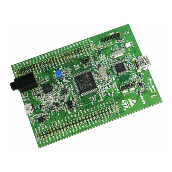
ST STM32F4 Series Getting Started
Mcu hardware development
Hide thumbs
Also See for STM32F4 Series:
- Programming manual (260 pages) ,
- Application note (50 pages) ,
- User manual (35 pages)
Table of Contents
Advertisement
Quick Links
Getting started with STM32F4xxxx MCU hardware development
Introduction
This application note is intended for system designers who require an overview of the
hardware implementation of the development board, with focus on features like
• power supply
• package selection
• clock management
• reset control
• boot mode settings
• debug management.
This document shows how to use the high-density high-performance microcontrollers listed
in
Table
1, and describes the minimum hardware resources required to develop an
application based on those products.
Detailed reference design schematics are also contained in this document, together with
descriptions of the main components, interfaces and modes.
Microcontrollers
March 2015
Table 1. Applicable products
Type
DocID026304 Rev 3
Application note
Part Number
STM32F401xB / STM32F401xC
STM32F401xD / STM32F401xE
STM32F405xx / STM32F407xx
STM32F411xC / STM32F411xE
STM32F415xx / STM32F417xx
STM32F427xx / STM32F429xx
STM32F437xx / STM32F439xx
STM32F446xx
AN4488
1/44
www.st.com
Advertisement
Table of Contents

Subscribe to Our Youtube Channel
Related Manuals for ST STM32F4 Series


Summary of Contents for ST STM32F4 Series
- Page 1 Table 1. Applicable products Type Part Number STM32F401xB / STM32F401xC STM32F401xD / STM32F401xE STM32F405xx / STM32F407xx STM32F411xC / STM32F411xE Microcontrollers STM32F415xx / STM32F417xx STM32F427xx / STM32F429xx STM32F437xx / STM32F439xx STM32F446xx March 2015 DocID026304 Rev 3 1/44 www.st.com...
-
Page 2: Table Of Contents
Contents AN4488 Contents Reference documents ........6 Power supplies . - Page 3 AN4488 Contents Boot mode selection ......... 30 Boot pin connection .
- Page 4 List of tables AN4488 List of tables Table 1. Applicable products ............1 Table 2.
- Page 5 AN4488 List of figures List of figures Figure 1. Power supply scheme............9 Figure 2.
-
Page 6: Reference Documents
The following documents are available on www.st.com. Table 2. Referenced documents Reference Title AN2867 Oscillator design guide for ST microcontrollers AN2606 STM32 microcontroller system memory boot mode AN3364 Migration and compatibility guidelines for STM32 microcontroller applications 6/44 DocID026304 Rev 3... -
Page 7: Power Supplies
AN4488 Power supplies Power supplies Introduction The operating voltage supply (V ) range is 1.8 V to 3.6 V, which can be reduced down to 1.7 V with some restrictions, as detailed in the product datasheets. An embedded regulator is used to supply the internal 1.2 V digital power. The real-time clock (RTC) and backup registers can be powered from the V voltage when the main V... -
Page 8: Voltage Regulator
Power supplies AN4488 2.1.3 Voltage regulator The voltage regulator is always enabled after reset. It works in three different modes depending on the application modes. • in Run mode, the regulator supplies full power to the 1.2 V domain (core, memories and digital peripherals) •... -
Page 9: Figure 1. Power Supply Scheme
AN4488 Power supplies Figure 1. Power supply scheme 1. Optional. If a separate, external reference voltage is connected on V , the two capacitors (100 nF and REF+ 1 µF) must be connected. 2. V is not available on all packages. In that case, a single 4.7 µF (ESR < 1Ω) is connected to V CAP2 CAP1 3. -
Page 10: Reset & Power Supply Supervisor
Power supplies AN4488 Reset & power supply supervisor 2.3.1 Power on reset (POR) / power down reset (PDR) The device has an integrated POR/PDR circuitry that allows proper operation starting from 1.8 V. The device remains in the Reset mode as long as V is below a specified threshold, , without the need for an external reset circuit. -
Page 11: System Reset
AN4488 Power supplies Figure 3. PVD thresholds 2.3.3 System reset A system reset sets all registers to their reset values except for the reset flags in the clock controller CSR register and the registers in the Backup domain (see Figure A system reset is generated when one of the following events occurs: A low level on the NRST pin (external reset) window watchdog end-of-count condition (WWDG reset) -
Page 12: Pdr_On Circuitry Example
NRST pin). Anyway (thanks to backward compatibility), circuitry built for other STM32F4xxxx products will work for STM32F411xx and STM32F446xx. Note: Please contact your local STMicroelectronics representative or visit www.st.com in case you want to use circuitry different from the one described hereafter. Restrictions: •... -
Page 13: Figure 6. Pdr_On Timings Example
AN4488 Power supplies Figure 6. PDR_ON timings example (not to scale, not needed for STM32F411xx and STM32F446xx) Selection of PDR_ON voltage supervisor Voltage supervisor should have the following characteristics • Reset output active-high push-pull (output driving high when voltage is below trip point) •... -
Page 14: Nrst Circuitry Example (For Stm32F411Xx And Stm32F446Xx Only)
Power supplies AN4488 2.3.5 NRST circuitry example (for STM32F411xx and STM32F446xx only) This example applies to STM32F411xx and STM32F446xx where PDR_ON can be connected to VSS to permanently disable internal reset circuitry. Restrictions: • PDR_ON = 0 is mostly intended for V supply between 1.7 V and 1.9V (i.e. -
Page 15: Figure 8. Nrst Circuitry Timings Example (Not To Scale, Only For Stm32F411Xx And Stm32F446Xx)
AN4488 Power supplies Figure 8. NRST circuitry timings example (not to scale, only for STM32F411xx and STM32F446xx) Selection of NRST voltage supervisor Voltage supervisor should have the following characteristics • Reset output active-low open-drain (output driving low when voltage is below trip point). -
Page 16: Regulator Off Mode
Power supplies AN4488 2.3.6 Regulator OFF mode Refer to section “Voltage regulator” in datasheet for details. • When BYPASS_REG = V , the core power supply should be provided through V CAP1 and V pins connected together. CAP1 – The two V ceramic capacitors should be replaced by two 100 nF decoupling capacitors. -
Page 17: Regulator On/Off And Internal Reset On/Off Availability
AN4488 Power supplies The following conditions must be respected: • should always be higher than V to avoid current injection between power domains. • If the time for V to reach V12 minimum value is smaller than the time for V reach 1.7 V, then PA0 should be kept low to cover both conditions: until V reaches V12 minimum value and until V... -
Page 18: Package
Package AN4488 Package Package Selection Package should be selected by taking into account the constrains that are strongly dependent upon the application. The list below summarizes the more frequent ones: – Amount of interfaces required. Some interfaces might not be available on some packages. Some interfaces combinations could not be possible on some packages –... -
Page 19: Table 5. Wcsp Package Summary
AN4488 Package Table 5. WCSP Package summary Sales numbers Number of balls Size (mm) Pitch (mm) Height (mm) STM32F405xx /407xx /415xx 4.258 x 4.004 0.62 /417xx STM32F42xxx / 43xxx 4.556 x 5.582 0.585 STM32F401xB/C 3 x 3 0.585 STM32F401xD/E 3.064 x 3.064 0.585 STM32F411xx 3.034 x 3.22... -
Page 20: Pinout Compatibility
Package AN4488 Pinout Compatibility Table 6 allows to select the right package depending on required signals. Note the two different pinouts for 64 and 100 pins which require specific connection in case board compatibility is required. See Table 10 and 11. Note that Chip Scale Package of different products even with same pinout might have different package dimensions which might be taken into account for PCB clearance. -
Page 21: Compatibility Within Stm32F4X Family
AN4488 Package Table 6. Pinout summary (continued) xQFP/xQFN xBGA xCSP Pin Name number of VSS VCAP1 VCAP2 1. Apply to STM32F405xx / F407xx / F415xx / F417xxx / F427xx / F429xx / F437xx / F439xx. 2. PB11 isn’t present on STM32F401xx / F411xx for 64 and 100 pins xQFP/xQFN packages. 3. -
Page 22: Figure 11. Stm32F4 Family Compatible Board Design For Lqfp100 Package
Package AN4488 Figure 11. STM32F4 family compatible board design for LQFP100 package Figure 12. Compatible board design STM32F4xx / STM32F446xx for LQFP144 package 22/44 DocID026304 Rev 3... -
Page 23: Compatibility With Stm32F1X And Stm32F2X Families
AN4488 Package 3.2.2 Compatibility with STM32F1x and STM32F2x families Figure 13. Compatible board design STM32F10xx/STM32F4xx for LQFP64 package Figure 14. Compatible board design STM32F10xx/STM32F2xx/STM32F4xx for LQFP100 package DocID026304 Rev 3 23/44... -
Page 24: For Lqfp144 Package
Package AN4488 Figure 15. Compatible board design STM32F10xx/STM32F2xx/STM32F4xx for LQFP144 package Figure 16. Compatible board design STM32F2xx and STM32F4xx for LQFP176 and UFBGA176 packages 24/44 DocID026304 Rev 3... -
Page 25: Alternate Function Mapping To Pins
AN4488 Package Alternate Function mapping to pins In order to easily explore Peripheral Alternate Functions mapping to pins, it is recommended to use the STM32CubeMX tool available on www.st.com. Figure 17. STM32CubeMX example screen-shot DocID026304 Rev 3 25/44... -
Page 26: Clocks
Clocks AN4488 Clocks Three different clock sources can be used to drive the system clock (SYSCLK): • HSI oscillator clock (high-speed internal clock signal) • HSE oscillator clock (high-speed external clock signal) • PLL clock The devices have two secondary clock sources: •... -
Page 27: External Source (Hse Bypass)
(10 pF can be used as a rough estimate of the combined pin and board capacitance). Refer to the dedicated Application Note (AN2867 - Oscillator design guide for ST microcontrollers) and electrical characteristics sections in the datasheet of your product for more details. -
Page 28: Lse Osc Clock
The load capacitance values must be adjusted according to the selected oscillator. Refer to the dedicated Application Note (AN2867 - Oscillator design guide for ST microcontrollers) and electrical characteristics sections in the datasheet of your product for more details. -
Page 29: Clock Security System (Css)
HSE oscillator. If the HSE oscillator clock (divided or not) is the clock entry of the PLL used as system clock when the failure occurs, the PLL is disabled too. For details, see the reference manuals available from the STMicroelectronics website www.st.com. DocID026304 Rev 3 29/44... -
Page 30: Boot Configuration
Boot configuration AN4488 Boot configuration Boot mode selection In the STM32F4xxxx, three different boot modes can be selected by means of the BOOT[1:0] pins as shown in Table Table 7. Boot modes BOOT mode selection pins Boot mode Aliasing BOOT1 BOOT0 Main Flash memory Main Flash memory is selected as boot space... -
Page 31: Embedded Boot Loader Mode
AN4488 Boot configuration Embedded boot loader mode The embedded boot loader is located in the System memory and is programmed by ST during production. For additional information, refer to AN2606 (Table 2 The USART peripheral operates with the internal 16 MHz oscillator (HSI). The CAN and USB OTG FS, however, can only function if an external clock (HSE) multiple of 1 MHz (between 4 and 26 MHz) is present. -
Page 32: Debug Management
Debug management AN4488 Debug management Introduction The Host/Target interface is the hardware equipment that connects the host to the application board. This interface is made of three components: a hardware debug tool, a JTAG or SW connector and a cable connecting the host to the debug tool. Figure 23 shows the connection of the host to the evaluation board. -
Page 33: Flexible Swj-Dp Pin Assignment
For more details, see the reference manual (Table 1), available from the STMicroelectronics website www.st.com. 6.3.3 Internal pull-up and pull-down resistors on JTAG pins The JTAG input pins must not be floating since they are directly connected to flip-flops to control the debug mode features. -
Page 34: Swj Debug Port Connection With Standard Jtag Connector
Debug management AN4488 To avoid any uncontrolled I/O levels, the STM32F4xxxx embeds internal pull-up and pull- down resistors on JTAG input pins: • JNTRST: Internal pull-up • JTDI: Internal pull-up • JTMS/SWDIO: Internal pull-up • TCK/SWCLK: Internal pull-down Once a JTAG I/O is released by the user software, the GPIO controller takes control again. The reset states of the GPIO control registers put the I/Os in the equivalent state: •... -
Page 35: Recommendations
AN4488 Recommendations Recommendations Printed circuit board For technical reasons, it is best to use a multilayer printed circuit board (PCB) with a separate layer dedicated to ground (V ) and another dedicated to the V supply. This provides good decoupling and a good shielding effect. For many applications, economical reasons prohibit the use of this type of board. -
Page 36: Other Signals
Recommendations AN4488 Figure 25. Typical layout for V pair Other signals When designing an application, the EMC performance can be improved by closely studying: • Signals for which a temporary disturbance affects the running process permanently (the case of interrupts and handshaking strobe signals, and not the case for LED commands). -
Page 37: Reference Design
AN4488 Reference design Reference design Description The reference design shown in Figure 26, is based on the STM32F407IG(H6), a highly ® integrated microcontroller running at 168 MHz, that combines the Cortex -M4 32-bit RISC CPU core with 1 Mbyte of embedded Flash memory and 192+4 Kbytes of SRAM including 64-Kbytes of CCM (core coupled memory) data RAM This reference design is intended to work with a V from 1.8V minimum (PDR_ON =... -
Page 38: Component References
Reference design AN4488 Component references Table 10. Mandatory components Id Components name Reference Quantity Comments 1 Microcontroller STM32F407IG(H6) UFBGA176 package 2 Capacitors 100 nF Ceramic capacitors (decoupling capacitors) 3 Capacitor 10 µF Ceramic capacitor (decoupling capacitor) Table 11. Optional components Id Components name Reference Quantity... -
Page 39: Figure 26. Stm32F407Ig(H6) Microcontroller Reference Schematic
AN4488 Reference design Figure 26. STM32F407IG(H6) microcontroller reference schematic 1. If no external battery is used in the application, it is recommended to connect V externally to V 2. To be able to reset the device from the tools this resistor has to be kept. DocID026304 Rev 3 39/44... -
Page 40: Table 12. Reference Connection For All Packages
Reference design AN4488 Table 12. Reference connection for all packages Pin Numbers for packages with Pin Numbers for BGA Chip Scale Packages pins on 4 edges Packages Pin Name PA13 A12 E12 A15 A15 PA14 A14 A14 PA15 A13 A13 A10 A10 PC14-OSC32_IN B10 D11... - Page 41 AN4488 Reference design Table 12. Reference connection for all packages (continued) Pin Numbers for packages with Pin Numbers for BGA Chip Scale Packages pins on 4 edges Packages Pin Name H13 G11 G13 F11 VCAP1 M10 L11 (30) (48) VCAP2 D12 F13 (31) (49)
- Page 42 Reference design AN4488 Table 12. Reference connection for all packages (continued) Pin Numbers for packages with Pin Numbers for BGA Chip Scale Packages pins on 4 edges Packages Pin Name H12 G10 (47) 1. Pins in parenthesis apply to STM32F401xx / F411xx 2.
-
Page 43: Revision History
AN4488 Revision history Revision history Table 13. Document revision history Date Revision Changes 20-Jun-2014 Initial release. Added STM32F411xC/xE in Table 1 Added footnote in Table 3 Updated Table 6 Table 12 28-Oct-2014 Updated Figure Figure 5 Figure 6 Updated Section 2.3.4 Added Section 2.3.5 for STM32F411xC/xE... - Page 44 ST products and/or to this document at any time without notice. Purchasers should obtain the latest relevant information on ST products before placing orders. ST products are sold pursuant to ST’s terms and conditions of sale in place at the time of order acknowledgement.
Need help?
Do you have a question about the STM32F4 Series and is the answer not in the manual?
Questions and answers