Table of Contents
Advertisement
UM1472
User manual
Discovery kit for STM32F407/417 lines
Introduction
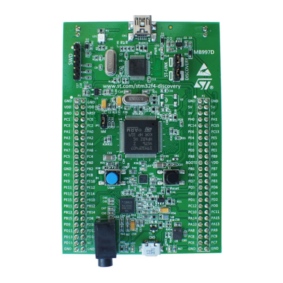
The STM32F4DISCOVERY helps you to discover the STM32F407 & STM32F417 lines'
high-performance features and to develop your applications.
It is based on an STM32F407VGT6 and includes an ST-LINK/V2 embedded debug tool
interface, ST MEMS digital accelerometer, ST MEMS digital microphone, audio DAC with
integrated class D speaker driver, LEDs, pushbuttons and a USB OTG micro-AB connector.
Figure 1. STM32F4DISCOVERY
1. Picture not contractual
January 2014
DocID022256 Rev 4
1/42
www.st.com
Advertisement
Table of Contents

Related Manuals for ST STM32F4DISCOVERY


Summary of Contents for ST STM32F4DISCOVERY
-
Page 1: Figure 1. Stm32F4Discovery
The STM32F4DISCOVERY helps you to discover the STM32F407 & STM32F417 lines’ high-performance features and to develop your applications. It is based on an STM32F407VGT6 and includes an ST-LINK/V2 embedded debug tool interface, ST MEMS digital accelerometer, ST MEMS digital microphone, audio DAC with integrated class D speaker driver, LEDs, pushbuttons and a USB OTG micro-AB connector. -
Page 2: Table Of Contents
Embedded ST-LINK/V2 ........ - Page 3 UM1472 List of tables List of tables Table 1. ON/OFF conventions ............5 Table 2.
- Page 4 STM32F4DISCOVERY connections image ........14...
-
Page 5: Conventions
UM1472 Conventions Conventions Table 1 provides the definition of some conventions used in the present document. Table 1. ON/OFF conventions Convention Definition Jumper JP1 ON Jumper fitted Jumper JP1 OFF Jumper not fitted Solder bridge SBx ON SBx connections closed by solder Solder bridge SBx OFF SBx connections left open DocID022256 Rev 4 5/42... -
Page 6: Quick Start
Check jumper position on the board, JP1 on, CN3 on (DISCOVERY selected). Connect the STM32F4DISCOVERY board to a PC with a USB cable ‘type A to mini-B’ through USB connector CN1 to power the board. Red LED LD2 (PWR) then lights up. -
Page 7: Features
STM32F407VGT6 microcontroller featuring 1 MB of Flash memory, 192 KB of RAM in an LQFP100 package • On-board ST-LINK/V2 with selection mode switch to use the kit as a standalone ST-LINK/V2 (with SWD connector for programming and debugging) • Board power supply: through USB bus or from an external 5V supply voltage •... -
Page 8: Hardware And Layout
Hardware and layout UM1472 Hardware and layout The STM32F4DISCOVERY is designed around the STM32F407VGT6 microcontroller in a 100-pin LQFP package. Figure 2 illustrates the connections between the STM32F407VGT6 and its peripherals (ST- LINK/V2, pushbutton, LED, Audio DAC, USB, ST MEMS accelerometer, ST MEMS microphone, and connectors). -
Page 9: Figure 3. Top Layout
UM1472 Hardware and layout Figure 3. Top layout Note: Pin 1 of CN2, CN3, JP1, P1 and P2 connectors are identified by a square. DocID022256 Rev 4 9/42... -
Page 10: Figure 4. Bottom Layout
Hardware and layout UM1472 Figure 4. Bottom layout 10/42 DocID022256 Rev 4... -
Page 11: Stm32F407Vgt6 Microcontroller
UM1472 Hardware and layout STM32F407VGT6 microcontroller This ARM Cortex-M4 32-bit MCU with FPU has 210 DMIPS, up to 1 MB Flash/192+4 KB RAM, USB OTG HS/FS, Ethernet, 17 TIMs, 3 ADCs, 15 comm. interfaces and a camera. Figure 5. STM32F407VGT6 package This device provides the following benefits. -
Page 12: Figure 6. Stm32F407Vgt6 Block Diagram
Hardware and layout UM1472 Figure 6. STM32F407VGT6 block diagram 12/42 DocID022256 Rev 4... -
Page 13: Embedded St-Link/V2
UM1472 Hardware and layout Embedded ST-LINK/V2 The ST-LINK/V2 programming and debugging tool is integrated on the STM32F4DISCOVERY. The embedded ST-LINK/V2 can be used in 2 different ways according to the jumper states (see Table • Program/debug the MCU on board, •... -
Page 14: Using St-Link/V2 To Program/Debug The Stm32F4 On Board
Hardware and layout UM1472 4.2.1 Using ST-LINK/V2 to program/debug the STM32F4 on board To program the STM32F4 on board, simply plug in the two jumpers on CN3, as shown in Figure 8 in red, but do not use the CN2 connector as that could disturb communication with the STM32F407VGT6 of the STM32F4DISCOVERY. -
Page 15: Using St-Link/V2 To Program/Debug An External Stm32 Application
Hardware and layout 4.2.2 Using ST-LINK/V2 to program/debug an external STM32 application It is very easy to use the ST-LINK/V2 to program the STM32 on an external application. Simply remove the 2 jumpers from CN3 as shown in Figure 9, and connect your application... -
Page 16: Power Supply And Power Selection
5V can also be used as input power supplies e.g. when the USB connector is not connected to the PC. In this case, the STM32F4DISCOVERY board must be powered by a power supply unit or by auxiliary equipment complying with standard EN-60950-1: 2006+A11/2009, and must be Safety Extra Low Voltage (SELV) with limited power capability. -
Page 17: On Board Audio Capability
• The sound can come independently from different inputs: – ST MEMS microphone (MP45DT02): digital using PDM protocol or analog when using the low pass filter. – USB connector: from external mass storage such as a USB key, USB HDD, and so on. -
Page 18: Jp1 (Idd)
Hardware and layout UM1472 JP1 (Idd) Jumper JP1, labeled Idd, allows the consumption of STM32F407VGT6 to be measured by removing the jumper and connecting an ammeter. • Jumper on: STM32F407VGT6 is powered (default). • Jumper off: an ammeter must be connected to measure the STM32F407VGT6 current, (if there is no ammeter, the STM32F407VGT6 is not powered). -
Page 19: Osc Clock
If PH0 and PH1 are only used as GPIOs instead of as a clock, then SB13 and SB14 are closed and R24, R25 and R68 are removed. • MCO from ST-LINK. From MCO of the STM32F103. This frequency cannot be changed, it is fixed at 8 MHz and connected to PH0-OSC_IN of the STM32F407VGT6. Configuration needed: –... -
Page 20: Solder Bridges
SB12 (SWO) SWO signal is not connected. No incidence on STM32F103C8T6 (ST-LINK/V2) NRST signal. SB10 (STM_RST) STM32F103C8T6 (ST-LINK/V2) NRST signal is connected to GND. BOOT0 signal of the STM32F407VGT6 MCU is held low through a 510 ohm pull-down resistor. SB18 (BOOT0) BOOT0 signal of the STM32F407VGT6 MCU is held high through a 10 Kohm pull-up resistor. -
Page 21: Extension Connectors
Hardware and layout 4.12 Extension connectors The male headers P1 and P2 can connect the STM32F4DISCOVERY to a standard prototyping/wrapping board. STM32F407VGT6 GPI/Os are available on these connectors. P1 and P2 can also be probed by an oscilloscope, logical analyzer or voltmeter. - Page 22 Hardware and layout UM1472 Table 5. MCU pin description versus board function (continued) MCU pin Board function Main Alternate function functions USART2_RX/ TIM5_CH4/ TIM9_CH2/ TIM2_CH4/ OTG_HS_ULPI_D0/ ETH_MII_COL/ ADC123_IN3 SPI1_NSS/ SPI3_NSS/ USART2_CK/ DCMI_HSYNC/ OTG_HS_SOF/ I2S3_WS/ ADC12_IN4/ DAC1_OUT SPI1_SCK/ OTG_HS_ULPI_CK/ TIM2_CH1_ETR/ TIM8_CHIN/ ADC12_IN5/ DAC2_OUT SPI1_MISO/...
- Page 23 UM1472 Hardware and layout Table 5. MCU pin description versus board function (continued) MCU pin Board function Main Alternate function functions MCO1/ USART1_CK/ TIM1_CH1/ I2C3_SCL/ OTG_FS_SOF USART1_TX/ TIM1_CH2/ I2C3_SMBA/ DCMI_D0/ OTG_FS_VBUS USART1_RX/ TIM1_CH3/ PA10 OTG_FS_ID/ DCMI_D1 USART1_CTS/ CAN1_RX/ PA11 TIM1_CH4/ OTG_FS_DM USART1_RTS/ CAN1_TX/...
- Page 24 Hardware and layout UM1472 Table 5. MCU pin description versus board function (continued) MCU pin Board function Main Alternate function functions TIM3_CH3/ TIM8_CH2N/ OTG_HS_ULPI_D1/ ETH_MII_RXD2/ TIM1_CH2N/ ADC12_IN8 TIM3_CH4/ TIM8_CH3N/ OTG_HS_ULPI_D2/ ETH_MII_RXD3/ OTG_HS_INTN/ TIM1_CH3N/ ADC12_IN9 JTDO/ TRACESWO/ SPI3_SCK/ I2S3_CK/ TIM2_CH2/ SPI1_SCK NJTRST/ SPI3_MISO/ TIM3_CH1/...
- Page 25 UM1472 Hardware and layout Table 5. MCU pin description versus board function (continued) MCU pin Board function Main Alternate function functions I2C1_SCL/ TIM4_CH1/ CAN2_TX/ OTG_FS_INTN/ DCMI_D5/ USART1_TX I2C1_SDA/ FSMC_NL/ DCMI_VSYNC/ USART1_RX/ TIM4_CH2 TIM4_CH3/ SDIO_D4/ TIM10_CH1/ DCMI_D6/ OTG_FS_SCL/ ETH_MII_TXD3/ I2C1_SCL/ CAN1_RX SPI2_NSS/ I2S2_WS/ TIM4_CH4/...
- Page 26 Hardware and layout UM1472 Table 5. MCU pin description versus board function (continued) MCU pin Board function Main Alternate function functions I2C2_SDA/ USART3_RX/ OTG_HS_ULPI_D4/ PB11 ETH_RMII_TX_EN/ ETH_MII_TX_EN/ OTG_HS_SDA/ TIM2_CH4 SPI2_NSS/ I2S2_WS/ I2C2_SMBA/ USART3_CK/ TIM1_BKIN/ PB12 CAN2_RX/ OTG_HS_ULPI_D5/ ETH_RMII_TXD0/ ETH_MII_TXD0/ OTG_HS_ID SPI2_SCK/ I2S2_CK/ USART3_CTS/...
- Page 27 UM1472 Hardware and layout Table 5. MCU pin description versus board function (continued) MCU pin Board function Main Alternate function functions SPI2_MOSI/ I2S2_SD/ TIM1_CH3N/ PB15 TIM8_CH3N/ TIM12_CH2/ OTG_HS_DP OTG_HS_ULPI_STP/ ADC123_IN10 ETH_MDC/ ADC123_IN11 SPI2_MISO/ OTG_HS_ULPI_DIR/ TH_MII_TXD2/ I2S2ext_SD/ ADC123_IN12 SPI2_MOSI/ I2S2_SD/ OTG_HS_ULPI_NXT/ ETH_MII_TX_CLK/ ADC123_IN13 ETH_RMII_RX_D0/...
- Page 28 Hardware and layout UM1472 Table 5. MCU pin description versus board function (continued) MCU pin Board function Main Alternate function functions I2S3_MCK/ TIM8_CH2/ SDIO_D7/ USART6_RX/ DCMI_D1/ TIM3_CH2 TIM8_CH3/ SDIO_D0/ TIM3_CH3/ USART6_CK/ DCMI_D2 I2S_CKIN/ MCO2/ TIM8_CH4/ SDIO_D1/ I2C3_SDA/ DCMI_D3/ TIM3_CH4 SPI3_SCK/ I2S3_CK/ UART4_TX/ PC10...
- Page 29 UM1472 Hardware and layout Table 5. MCU pin description versus board function (continued) MCU pin Board function Main Alternate function functions PC13 RTC_AF1 PC14 OSC32_IN PC15 OSC32_OUT FSMC_D2/ CAN1_RX FSMC_D3/ CAN1_TX TIM3_ETR/ UART5_RXSDIO_CMD DCMI_D11 FSMC_CLK/ USART2_CTS FSMC_NOE/ USART2_RTS FSMC_NWE/ USART2_TX FSMC_NWAIT/ USART2_RX USART2_CK/...
- Page 30 Hardware and layout UM1472 Table 5. MCU pin description versus board function (continued) MCU pin Board function Main Alternate function functions FSMC_D13/ USART3_TX FSMC_D14/ USART3_RX FSMC_D15/ PD10 USART3_CK FSMC_A16/ PD11 USART3_CTS FSMC_A17/ PD12 TIM4_CH1/ USART3_RTS FSMC_A18/ PD13 TIM4_CH2 FSMC_D0/ PD14 TIM4_CH3 FSMC_D1/ PD15...
- Page 31 UM1472 Hardware and layout Table 5. MCU pin description versus board function (continued) MCU pin Board function Main Alternate function functions TRACED1/ FSMC_A20/ DCMI_D4 TRACED2/ FSMC_A21/ TIM9_CH1/ DCMI_D6 TRACED3/ FSMC_A22/ TIM9_CH2/ DCMI_D7 FSMC_D4/ TIM1_ETR FSMC_D5/ TIM1_CH1N FSMC_D6/ TIM1_CH1 FSMC_D7/ PE10 TIM1_CH2N FSMC_D8/ PE11...
- Page 32 Hardware and layout UM1472 Table 5. MCU pin description versus board function (continued) MCU pin Board function Main Alternate function functions OSC_OUT 32/42 DocID022256 Rev 4...
- Page 33 UM1472 Hardware and layout Table 5. MCU pin description versus board function (continued) MCU pin Board function Main Alternate function functions DocID022256 Rev 4 33/42...
-
Page 34: Mechanical Drawing
Mechanical drawing UM1472 Mechanical drawing Figure 10. STM32F4DISCOVERY mechanical drawing 34/42 DocID022256 Rev 4... -
Page 35: Electrical Schematics
UM1472 Electrical schematics Electrical schematics Figure 11. STM32F4DISCOVERY DocID022256 Rev 4 35/42... -
Page 36: Figure 12. St-Link/V2 (Swd Only)
Electrical schematics UM1472 Figure 12. ST-LINK/V2 (SWD only) 36/42 DocID022256 Rev 4... -
Page 37: Figure 13. Mcu
UM1472 Electrical schematics Figure 13. MCU DocID022256 Rev 4 37/42... -
Page 38: Figure 14. Audio
Electrical schematics UM1472 Figure 14. Audio 38/42 DocID022256 Rev 4... -
Page 39: Figure 15. Usb_Otg_Fs
UM1472 Electrical schematics Figure 15. USB_OTG_FS DocID022256 Rev 4 39/42... -
Page 40: Figure 16. Peripherals
Electrical schematics UM1472 Figure 16. Peripherals 40/42 DocID022256 Rev 4... -
Page 41: Revision History
Figure 2 Chapter 6: Electrical schematics. Modified Table 5 PE2 and PE3 entries. Updated for board rev. C. Modified title. Modified Section 4.8: Motion sensor (ST MEMS LIS302DL or 28-Nov-2013 LIS3DSH) Updated Chapter 6: Electrical schematics Modified Chapter 3: Features, Figure Chapter 4.8: Motion sensor... - Page 42 No license, express or implied, by estoppel or otherwise, to any intellectual property rights is granted under this document. If any part of this document refers to any third party products or services it shall not be deemed a license grant by ST for the use of such third party products or services, or any intellectual property contained therein or considered as a warranty covering the use in any manner whatsoever of such third party products or services or any intellectual property contained therein.
Need help?
Do you have a question about the STM32F4DISCOVERY and is the answer not in the manual?
Questions and answers