Sign In
Upload
Manuals
Brands
Fujitsu Manuals
Computer Hardware
F2MC-16LX Series
Fujitsu F2MC-16LX Series Manuals
Manuals and User Guides for Fujitsu F2MC-16LX Series. We have
10
Fujitsu F2MC-16LX Series manuals available for free PDF download: Hardware Manual, Application Note, User Manual
Fujitsu F2MC-16LX Series Hardware Manual (706 pages)
16-bit Microcontroller MB90330 series
Brand:
Fujitsu
| Category:
Microcontrollers
| Size: 13.48 MB
Table of Contents
9
Table of Contents
17
Chapter 1 Overview
18
Feature of MB90330 Series
23
Block Diagram
24
Package Dimension
26
Pin Assignment
27
Pin Function
34
I/O Circuit Types
37
Handling of Device
41
Chapter 2 Cpu
42
Outline Specification of CPU
43
Memory Space
48
Register of CPU
50
Accumulator (A)
51
User Stack Pointer (USP) and System Stack Pointer (SSP)
52
Processor Status (PS)
55
Program Counter (PC)
56
Program Bank Register (PCB)
57
Direct Page Register (DPR)
58
General-Purpose Registers (Register Bank)
59
Prefix Code
63
Chapter 3 Interrupt
64
Outline of Interrupt
67
Interrupt Cause and Interrupt Vector
70
Interrupt Control Register and Peripheral Function
72
Interrupt Control Registers (ICR00 to ICR15)
74
Interrupt Control Register Functions
77
Hardware Interrupt
80
Operation of Hardware Interrupt
82
Operation Flow of Hardware Interrupt
83
Procedure for Using a Hardware Interrupt
84
Multiple Interrupts
86
Hardware Interrupt Processing Time
88
Software Interrupt
90
Interrupts By Extended Intelligent I/O Service (EI 2 OS)
92
Extended Intelligent I/O Service
92
OS) Descriptor (ISD)
94
Each Register of Extended Intelligent I/O Service
94
OS) Descriptor (ISD)
97
Operation of Extended Intelligent I/O Service (EI 2 OS)
98
Procedure for Use of Extended Intelligent I/O Service (EI 2 OS)
99
OS) Processing Time
102
Exception Processing Interrupt
103
Interruption By Μdmac
104
Μdmac Function
105
Register of Μdmac
106
DMA Descriptor Channel Specification Register (DCSR)
108
DMA Status Register (DSRH/DSRL)
109
DMA Stop Status Register (DSSR)
110
DMA Permission Register (DERH/DERL)
111
DMA Descriptor Window Register (DDWR)
112
DMA Data Counter (DDCTH/DDCTL)
113
DMA I/O Register Address Pointer (DIOAH/DIOAL)
114
DMA Control Register (DMACS)
116
DMA Buffer Address Pointer (DBAPH/DBAPM/DBAPL)
117
Explanation of Operation of Μdmac
119
Exceptions
120
Stack Operation of Interrupt Processing
122
Program Example of Interrupt Processing
126
Delayed Interrupt Generation Module
127
Operation of Delayed Interrupt Generation Module
129
Chapter 4 Reset
130
Outline of Reset
132
Reset Factors and Oscillation Stabilization Wait Times
134
External Reset Pin
135
Reset Operation
137
Reset Factor Bit
139
State of Each Pin at Reset
141
Chapter 5 Clock
142
Outline of Clock
145
Block Diagram of Clock Generation Section
148
Clock Select Register (CKSCR)
151
Clock Mode
154
Oscillation Stabilization Wait Time
155
Connection of Oscillator and External Clock
157
Chapter 6 Low-Power Consumption Mode
158
Outline of Low-Power Consumption Mode
161
Block Diagram of Low-Power Consumption Control Circuit
163
Low-Power Consumption Mode Control Register (LPMCR)
166
CPU Intermittent Operation Mode
167
Standby Mode
168
Sleep Mode
170
Timebase Timer Mode
172
Watch Mode
174
Stop Mode
176
State Transition Diagram
178
State of the Pin During Standby Mode, Hold, and Reset
188
Precautions When Using Low-Power Consumption Mode
191
Chapter 7 Mode Setting
192
Mode Setting
193
Mode Pins (MD2 to MD0)
194
Mode Data
198
External Memory Access
200
Automatic Ready Function Selection Register (ARSR)
201
External Address Output Control Register (HACR)
202
Bus Control Signal Selection Register (EPCR)
204
Operation in Each Mode of Mode Setting
205
External Memory Access Control Signal
208
Ready Function
211
Holding Function
213
Chapter 8 I/O Port
214
Functions of I/O Ports
215
I/O Port Register
216
Port Data Register (PDR0 to PDRB)
217
Port Direction Register (DDR0 to DDRB)
218
Other Registers
221
Chapter 9 Timebase Timer
222
Overview of Timebase Timer
224
Configuration of Timebase Timer
226
Timebase Timer Control Register (TBTC)
228
Interrupt of Timebase Timer
229
Operations of Timebase Timer
231
Precautions When Using Timebase Timer
233
Program Example of Timebase Timer
235
Chapter 10 Watchdog Timer
236
Overview of Watchdog Timer
238
Watchdog Timer Control Register (WDTC)
240
Configuration of Watchdog Timer
242
Operations of Watchdog Timer
244
Precautions When Using Watchdog Timer
245
Program Examples of Watchdog Timer
247
Chapter 11 Watch Timer
248
Overview of Watch Timer
249
Configuration of Watch Timer
250
Watch Timer Control Register (WTC)
252
Operation of Watch Timer
254
Chapter 12 16-Bit I/O Timer
254
Overview of 16-Bit I/O Timer
256
Register of 16-Bit I/O Timer
257
16-Bit Free-Run Timer
263
Output Compare
268
Input Capture
271
Operation of 16-Bit I/O Timer
272
Operation of 16-Bit Free-Run Timer
274
Operation of 16-Bit Output Compare
276
Operation of 16-Bit Input Capture
277
Timing of 16-Bit Free-Run Timer
278
Output Compare Timing
279
Input Timing of Input Capture
Advertisement
Fujitsu F2MC-16LX Series Hardware Manual (710 pages)
16 Bit, Controller Manual
Brand:
Fujitsu
| Category:
Microcontrollers
| Size: 12.52 MB
Table of Contents
11
Table of Contents
19
Chapter 1 Overview
20
Features of the MB90895 Series
22
Product Lineup for MB90895 Series
25
Block Diagram of MB90895 Series
26
Pin Assignment
27
Package Dimensions
28
Pin Description
31
I/O Circuit
33
Chapter 2 Handling Devices
34
Precautions When Handling Devices
37
Chapter 3 Cpu
38
Memory Space
40
Mapping of and Access to Memory Space
42
Memory Map
43
Addressing
44
Linear Addressing
45
Bank Addressing
47
Allocation of Multi-Byte Data in Memory
49
Dedicated Registers
51
Dedicated Registers and General-Purpose Register
52
Accumulator (A)
55
Stack Pointer (USP, SSP)
58
Processor Status (PS)
63
Program Counter (PC)
64
Direct Page Register (DPR)
65
Bank Register (PCB, DTB, USB, SSB, and ADB)
66
General-Purpose Register
68
Prefix Code
69
Bank Select Prefix (PCB, DTB, ADB, and SPB)
71
Common Register Bank Prefix (CMR)
72
Flag Change Inhibit Prefix (NCC)
73
Restrictions on Prefix Code
75
Interrupt
77
Interrupt Factor and Interrupt Vector
80
Interrupt Control Registers and Peripherals
82
Interrupt Control Register (ICR00 to ICR15)
84
Function of Interrupt Control Register
87
Hardware Interrupt
90
Operation of Hardware Interrupt
92
Procedure for Use of Hardware Interrupt
93
Multiple Interrupts
95
Software Interrupt
96
Interrupts by Extended Intelligent I/O Service (EI 2 OS)
98
EI os Descriptor (ISD)
100
Each Register of EI 2 os Descriptor (ISD)
103
Operation of EI 2 os
104
Procedure for Use of EI 2 os
105
EI 2 os Processing Time
107
Exception Processing Interrupt
108
Time Required to Start Interrupt Processing
110
Stack Operation for Interrupt Processing
111
Program Example of Interrupt Processing
114
Reset
116
Reset Factors and Oscillation Stabilization Wait Times
118
External Reset Pin
119
Reset Operation
121
Reset Factor Bit
124
State of each Pin at Reset
125
Clock
128
Block Diagram of Clock Generation Section
130
Register in Clock Generation Section
131
Clock Select Register (CKSCR)
134
Pll/Subclock Control Register (PSCCR)
136
Clock Mode
140
Oscillation Stabilization Wait Time
141
Connection of Oscillator and External Clock
142
Low-Power Consumption Mode
145
Block Diagram of Low-Power Consumption Circuit
147
Registers for Setting Low-Power Consumption Modes
148
Low-Power Consumption Mode Control Register (LPMCR)
151
CPU Intermittent Operation Mode
152
Standby Mode
163
State Transition in Standby Mode
164
Pin State in Standby Mode, at Reset
165
Precautions When Using Low-Power Consumption Mode
169
CPU Mode
170
Mode Pins (MD2 to MD0)
172
Mode Data
174
Memory Access Mode
175
Operations for Selecting Memory Access Mode
177
Chapter 4 I/O Port
178
Overview of I/O Ports
179
Registers of I/O Port and Assignment of Pins Serving as External Bus
180
Port 1
182
Registers for Port 1 (PDR1, DDR1)
183
Operation of Port 1
185
Port2
188
Registers for Port 2 (PDR2, DDR2)
189
Operation of Port 2
191
Port 3
193
Registers for Port 3 (PDR3, DDR3)
194
Operation of Port 3
196
Port 4
198
Registers for Port 4 (PDR4, DDR4)
199
Operation of Port 4
201
Port 5
204
Registers for Port 5 (PDR5, DDR5, ADER)
206
Operation of Port 5
208
Port Input Level Select Register
209
CHAPTER 5 Timebase Timer
210
Overview of Timebase Timer
212
Block Diagram of Timebase Timer
214
Configuration of Timebase Timer
215
Timebase Timer Control Register (TBTC)
217
Interrupt of Timebase Timer
218
Explanation of Operations of Timebase Timer Functions
222
Precautions When Using Timebase Timer
223
Program Example of Timebase Timer
225
CHAPTER 6 Watchdog Timer
226
Overview of Watchdog Timer
227
Configuration of Watchdog Timer
229
Watchdog Timer Registers
230
Watchdog Timer Control Register (WDTC)
232
Explanation of Operations of Watchdog Timer Functions
235
Precautions When Using Watchdog Timer
236
Program Examples of Watchdog Timer
237
16-Bit I/O Timer
238
Overview of 16-Bit Input/Output Timer
239
Block Diagram of 16-Bit Input/Output Timer
240
Block Diagram of 16-Bit Free-Run Timer
242
Block Diagram of Input Capture
244
Configuration of 16-Bit Input/Output Timer
247
Timer Counter Control Status Register (TCCS)
249
Timer Counter Data Register (TCDT)
251
Input Capture Control Status Registers (ICS01, ICS23)
253
Input Capture Data Registers (IPCP0 to IPCP3)
254
Interrupts of 16-Bit Input/Output Timer
255
Explanation of Operation of 16-Bit Free-Run Timer
257
Explanation of Operation of Input Capture
260
Precautions When Using 16-Bit Input/Output Timer
261
Program Example of 16-Bit Input/Output Timer
263
16-Bit Reload Timer
264
Overview of 16-Bit Reload Timer
267
Block Diagram of 16-Bit Reload Timer
270
Configuration of 16-Bit Reload Timer
273
Timer Control Status Registers (High) (TMCSR0: H, TMCSR1: H)
275
Timer Control Status Registers (High) (TMCSR0: H, TMCSR1: H)
277
16-Bit Timer Registers (TMR0, TMR1)
278
16-Bit Reload Registers (TMRLR0, TMRLR1)
279
Interrupts of 16-Bit Reload Timer
280
Explanation of Operation of 16-Bit Reload Timer
282
Operation in Internal Clock Mode
287
Operation in Event Count Mode
290
Precautions When Using 16-Bit Reload Timer
291
Program Example of 16-Bit Reload Timer
Fujitsu F2MC-16LX Series Hardware Manual (395 pages)
16-Bit Microcontrollers
Brand:
Fujitsu
| Category:
Microcontrollers
| Size: 3.4 MB
Table of Contents
5
Table of Contents
21
Chapter 1 Overview
21
Features
23
Product Lineup
23
Table 1.2A MB90580 Series Product Lineup
24
Block Diagram
24
Chapter 1 Overview
24
Figure 1.3A Block Diagram of MB90580 Series
25
Pin Assignment
25
SQFP-100 Pin Assignment
25
Figure 1.4A Pin Assignment of MB90580 (LQFP-100)
26
Pin Assignment
26
Figure 1.4B Pin Assignment of MB90580 (QFP-100)
27
Pin Functions
27
Table 1.5A Pin Functions (1/4) (STBC: with Standby Control)
28
Table 1.5B Pin Functions (2/4)
29
Table 1.5C Pin Functions (3/4)
30
Table 1.5D Pin Functions (4/4)
31
Table 1.5E I/O Circuit Format (1)
32
Table 1.5F I/O Circuit Format (2)
33
Table 1.5G I/O Circuit Format (3)
34
Figure 1.6A Using External Clock
34
Figure 1.6B Connection of Power Pins
34
Handling the Device
35
Chapter 2 CPU
35
Cpu
36
Memory Space
36
Figure 2.1.1A Sample Relationship Between F2MC-16LX System and Memory Map
37
Figure 2.1.1B Sample Linear Addressing
38
Figure 2.1.1C Physical Addresses of Each Space
38
Table 2.1.1A Default Space
39
Figure 2.1.1D Sample Allocation of Multi-Byte Data in Memory
39
Figure 2.1.1E Execution of MOVW A, 080FFFFH
40
Registers
40
Figure 2.1.2A Special Registers
41
Figure 2.1.2B General-Purpose Registers
41
Figure 2.1.2C Program Counter
42
Figure 2.1.2D 32-Bit Data Transfer
42
Figure 2.1.2E AL-AH Transfer
43
Figure 2.1.2F Stack Manipulation Instruction and Stack Pointer
44
Figure 2.1.2G PS Structure
44
Figure 2.1.2H Condition Code Register Configuration
45
Figure 2.1.2I Register Bank Pointer
45
Figure 2.1.2J Interrupt Level Register
45
Chapter 2 CPU
45
Table 2.1.2A Levels Indicated By the Interrupt Level Mask (ILM) Register
46
Table 2.1.2B Register Functions
46
Table 2.1.2C Relationship Between Registers
47
Figure 2.1.2K Generating a Physical Address in Direct Addressing Mode
48
Prefix Codes
48
Table 2.1.3A Bank Select Prefix
49
Figure 2.1.3A Interrupt Disable Instruction
50
Figure 2.1.3B Interrupt Disable Instructions and Prefix Codes
50
Figure 2.1.3C Consecutive Prefix Codes
51
Chapter 3 Memory
51
Memory Access Modes
51
Table 3.1A Memory Access Mode
52
Mode Pins
52
Table 3.1.1A Mode Pins and Modes
53
Mode Data
54
Bus Mode
54
Figure 3.1.3A Access Areas and Physical Addresses in Each Bus Mode
55
Chapter 3 Memory
55
Table 3.1.3A Sample Recommended Setting of Mode Pins and Mode Data
55
Table 3.1.3B Modes and Related External Pin Operations
56
External Memory Access
56
Block Diagram
56
Figure 3.2.1A External Bus Pin Control Circuit
57
Registers and Register Details
59
Table 3.2.0A Selecting the High-Order Address Bit Output Control
62
Operations
62
Figure 3.2.1A External Memory Access Timing Chart
63
Figure 3.2.1B External Memory Access Timing Chart
64
Figure 3.2.1C Ready Timing Chart
65
Figure 3.2.1D Hold Timing
67
Chapter 4 Clock and Reset
67
Clock Generator
67
Figure 4.1A Clock Generator Circuit Block Diagram
68
Reset Causes
68
Table 4.2A Reset Causes
69
Figure 4.2A Reset Cause Bit Block Diagram
69
Figure 4.2B WDTC (Watch-Dog Timer Control Register)
69
Table 4.2B Reset Cause Bits
70
Operation After Reset Release
70
Figure 4.3A Source and Destination of Reset Vector and Mode Data
71
Chapter 5 Watchdog Timer, Timebase Timer, and Watch Timer Functions
71
Outline
72
Block Diagram
72
Chapter 5 Watchdog Timer, Timebase Timer, and Watch Timer Functions
72
Figure 5.2A Watchdog Timer, Timebase Timer, and Watch Timer Block Diagram
73
Registers and Register Details
74
WDTC (Watch-Dog Timer Control Register)
74
Table 5.3.1A Reset Cause Registers
75
Table 5.3.1B Watchdog Timer Interval Selection Bits
76
TBTC (Time Base Timer Control Register)
76
Table 5.3.2A Selecting the Time Base Timer Interval
77
Watch Timer Control Register (WTC)
78
Table 5.3.3A Watch Timer Interval Selection
79
Operation
79
Watch-Dog Timer
79
Figure 5.4.1A Watch-Dog Timer Operation
80
Time Base Timer
80
Watch Timer
81
Chapter 6 Low Power Control Circuit
81
Outline
82
Block Diagram
82
Figure 6.2A Low-Power Consumption Control Circuit and Clock Generator
83
Chapter 6 Low Power Control Circuit
83
Registers and Register Details
83
LPMCR (Low Power Mode Control Register)
84
Table 6.3.1A CG Bit Setting
85
CKSCR (Clock Selection Register)
85
Table 6.3.2A WS Bit Settings
86
Table 6.3.2B CS Bit Settings
87
Operations
87
Table 6.4A Low Power Consumption Mode Operating Statuses
88
Pseudo-Watch Mode
88
Sleep Mode
89
Stop Mode
89
Watch Mode
90
CPU Intermittent Operation Function
90
Hardware Standby Mode
91
Setting the Main Clock Oscillation Stabilization Waiting Period
91
Switching the Machine Clock
92
Figure 6.4.8A Clock Selection State Transition Diagram (1)
93
Figure 6.4.8B Clock Selection State Transition Diagram (2)
93
State Transition
94
Table 6.4.9A List of Transition Conditions
96
Chapter 7 Interrupt
97
Figure 6.4.9A Low Power Consumption Mode Transition Diagram a
98
Figure 6.4.9B Low Power Consumption Mode Transition Diagram B
99
Figure 6.4.9C Low Power Consumption Mode Transition Diagram C
100
Figure 6.4.9D Low Power Consumption Mode Transition Diagram D
101
Chapter 7 Interrupt
101
Outline
102
Causes of Interrupt
102
Table 7.2A Interrupt Causes, Interrupt Vectors, and Interrupt Control Registers
103
Interrupt Vector
103
Table 7.3A MB90580 Interrupt Assignment Table (1/2)
104
Hardware Interrupt
104
Overview
104
Structure
104
Operation
105
Figure 7.4.3A Occurrence and Release of Hardware Interrupt
106
Figure 7.4.3B Hardware Interrupt Operation Flow
106
Table 7.4.3A Compensation Values for Interrupt Processing Cycle Count
107
Hardware Interrupt Ocurrence When Internal Resource Is Being Accessed
107
Interrupt Inhibit Instruction
107
Multiple Interrupts
107
Register Saving in Stack Upon Interrupt
107
Precaution in Using Hardware Interrupt
107
Figure 7.4.7A Registers Saved in Stack
108
Software Interrupt
108
Overview
108
Structure
109
Operation
109
Others
109
Figure 7.5.3A Occurrence and Release of Software Interrupt
110
Extended Intelligent I/O Service (EI2OS)
110
Overview
110
Figure 7.6.1A Outline of Extended Intelligent I/O Service
111
Structure
112
Table 7.6.2A ICS Bits, Channel Numbers, and Descriptor Addresses
112
Table 7.6.2B S Bits and End Conditions
113
Table 7.6.2C Interrupt Level Setting Bits and Interrupt Levels
114
Figure 7.6.2A Extended Intelligent I/O Service Descriptor Configuration
117
Operation
117
Figure 7.6.3A EI2OS Operation Flow
118
Figure 7.6.3B EI2OS Use Flow
119
EI2OS Execution Time
119
Table 7.6.4A Execution Time When the Extended I2OS Continues
119
Table 7.6.4B Data Transfer Compensation Values for Extended I2OS Execution Time
120
Exceptions
120
Exception Due to Execution of an Undefined Instruction
121
Chapter 8 Parallel Ports
121
Outline
122
Block Diagram
122
Figure 8.2A Block Diagram of I/O Port
122
Figure 8.2B Block Diagram of Input Resistor Register
122
Figure 8.2C Block Diagram of Output Pin Register
123
Registers and Register Details
123
Figure 8.3A Registers of Parallel Ports
124
Port Data Register
125
Port Direction Registers
126
Input Resistor Register
126
Output Pin Register
127
Analogue Input Enable Register
127
Low Noise Output Select Register
129
Chapter 9 Dtp/External Interrupt
129
Outline
129
Block Diagram
129
Figure 9.2A Block Diagram of Dtp/External Interrupt
130
Registers and Register Details
130
Interrupt/Dtp Enable Register (ENIR: Enable Interrupt Request Register)
131
Interrupt/Dtp Cause Register (EIRR: External Interrupt Request Register)
131
Request Level Setting Register (ELVR: External Level Register)
132
Operations
132
External Interrupts
132
Figure 9.4.1A External Interrupt
133
DTP Operation
133
Figure 9.4.2A Timing to Cancel the External Interrupt at the End of DTP Operation
133
Figure 9.4.2B Sample Interface to the External Peripheral
134
Switching Between External Interrupt and DTP Requests
134
Figure 9.4.3A Switching Between External Interrupt and DTP Requests
135
Notes On Use
135
Conditions On the Externally Connected Peripheral When DTP Is Used
135
Recovery From Standby
135
External Interrupt/Dtp Operation Procedure
135
External Interrupt Request Level
135
Figure 9.5.4A Clearing the Cause Hold Circuit Upon Level Set
137
Chapter 10 Delayed Interrupt Generation Module
137
Outline
137
Block Diagram
137
Registers and Register Details
137
Figure 10.2A Block Diagram of Delayed Interrupt Generation Module
138
Operations
138
Delayed Interrupt Occurrence
138
Notes On Operation
138
Delayed Interrupt Request Lock
138
Figure 10.4.1A Delayed Interrupt Issuance
139
Chapter 11 Communication Prescaler
139
Outline
139
Block Diagram
139
Figure 11.2A Block Diagram of Communication Prescaler
140
Register and Register Details
140
Clock Division Control Registers
141
Operations
Advertisement
Fujitsu F2MC-16LX Series Hardware Manual (635 pages)
16-BIT MICROCONTROLLER
Brand:
Fujitsu
| Category:
Microcontrollers
| Size: 7.23 MB
Table of Contents
10
Table of Contents
22
Chapter 1 Overview
23
Feature of MB90335 Series
28
Block Diagram
29
Package Dimension
30
1.4 Pin Assignment
31
Pin Function
34
I/O Circuit Types
37
Handling of Device
40
Chapter 2 Cpu
41
Overview of the CPU
42
Memory Space
45
Linear Addressing
46
Bank Addressing
48
Multibyte Data in Memory Space
49
Registers
52
Accumulator (A)
53
User Stack Pointer (USP) and System Stack Pointer (SSP)
54
Processor Status (PS)
57
Program Counter (PC)
58
Bank Registers (PCB, DTB, USB, SSB, ADB)
59
Direct Page Register (DPR)
60
Register Bank
61
Prefix Codes
64
Interrupt Disable Instructions
66
Chapter 3 Interrupt
67
Outline of Interrupt
70
Interrupt Cause and Interrupt Vector
73
Interrupt Control Register and Peripheral Function
75
Interrupt Control Registers (ICR00 to ICR15)
77
Interrupt Control Register Functions
80
Hardware Interrupt
83
Operation of Hardware Interrupt
85
Operation Flow of Hardware Interrupt
86
Procedure for Using a Hardware Interrupt
87
Multiple Interrupts
89
Hardware Interrupt Processing Time
91
Software Interrupt
93
Interrupts by Extended Intelligent I/O Service (EI 2 OS)
95
Extended Intelligent I/O Service (EI 2 OS) Descriptor (ISD)
97
OS) Descriptor (ISD)
100
Operation of Extended Intelligent I/O Service (EI 2 OS)
101
Procedure for Use of Extended Intelligent I/O Service (EI 2 OS)
102
Extended Intelligent I/O Service (EI 2 OS) Processing Time
105
Exception Processing Interrupt
106
Interruption by Μdmac
107
Μdmac Function
108
Register of Μdmac
115
DMA Descriptor Window Register (DDWR)
121
Explanation of Operation of Μdmac
123
Exceptions
124
Stack Operation of Interrupt Processing
126
Program Example of Interrupt Processing
130
Delayed Interrupt Generation Module
131
Operation of Delayed Interrupt Generation Module
132
Chapter 4 Reset
133
Outline of Reset
135
Reset Factors and Oscillation Stabilization Wait Times
137
External Reset Pin
138
Reset Operation
140
Reset Factor Bit
142
State of each Pin at Reset
144
Chapter 5 Clock
145
Outline of Clock
147
Block Diagram of Clock Generation Section
149
Clock Select Register (CKSCR)
151
Clock Mode
153
Oscillation Stabilization Wait Time
154
Connection of Oscillator and External Clock
156
Chapter 6 Low-Power Consumption Mode
157
Outline of Low-Power Consumption Mode
160
Block Diagram of Low-Power Consumption Control Circuit
162
Low-Power Consumption Mode Control Register (LPMCR)
165
CPU Intermittent Operation Mode
166
Standby Mode
167
Sleep Mode
169
Time-Base Timer Mode
170
Stop Mode
172
State Transition Diagram
174
State of the Pin During Standby Mode, and Reset
175
Precautions When Using Low-Power Consumption Mode
178
Chapter 7 Mode Setting
179
Mode Setting
180
Mode Pins (MD2 to MD0)
181
Mode Data
184
Chapter 8 I/O Port
185
Functions of I/O Ports
186
I/O Port Register
187
Port Data Register (PDR0 to PDR2, PDR4 to PDR6)
188
Port Direction Register (DDR0 to DDR2, DDR4 to DDR6)
189
Other Registers
190
Chapter 9 Time-Base Timer
191
Overview of Time-Base Timer
193
Configuration of Time-Base Timer
195
Time-Base Timer Control Register (TBTC)
197
Interrupt of Time-Base Timer
198
Operations of Time-Base Timer
200
Precautions When Using Time-Base Timer
202
Program Example of Time-Base Timer
204
Chapter 10 Watchdog Timer
205
Overview of Watchdog Timer
206
Watchdog Timer Control Register (WDTC)
208
Configuration of Watchdog Timer
209
Operations of Watchdog Timer
211
Precautions When Using Watchdog Timer
212
Program Examples of Watchdog Timer
214
Chapter 11 Usb Function
215
Overview of USB Function
216
Block Diagram of USB Function
217
Registers of USB Function
220
UDC Control Register (UDCC)
223
EP0 Control Register (EP0C)
225
EP1 to EP5 Control Register (EP1C to EP5C)
229
Time Stamp Register (TMSP)
230
UDC Status Register (UDCS)
233
UDC Interruption Enable Register (UDCIE)
235
EP0I Status Register (EP0IS)
237
EP0O Status Register (EP0OS)
240
EP1 to EP5 Status Register (EP1S to EP5S)
244
EP0 to EP5 Data Register (EP0DT to EP5DT)
245
Operation Explanation of USB Function
248
Detecting Connection and Disconnection
250
Each Register Operation When Command Responds
252
STALL Response and Release
256
Suspend Function
257
Wake-Up Function
258
DMA Transfer Function
262
NULL Transfer Function
Fujitsu F2MC-16LX Series Hardware Manual (598 pages)
MB90470 Series 16-BIT MICROCONTROLLER
Brand:
Fujitsu
| Category:
Microcontrollers
| Size: 16.23 MB
Table of Contents
9
Table of Contents
17
Chapter 1 Overview of Mb90470
18
Overview
21
Block Diagram of MB90470
22
Package Dimensions
24
Pin Assignment
26
Pin Functions
32
I/O Circuit Type
35
Handling the Device
37
Chapter 2 Cpu
38
Overview of CPU Specifications
39
Memory Space
43
CPU Registers
45
Accumulator (A)
46
User Stack Pointer (USP) and System Stack Pointer (SSP)
47
Processor Status (PS)
50
Program Counter (PC)
51
Program Count Bank Register (PCB)
52
Direct Page Register (DPR)
53
General-Purpose Register (Register Bank)
54
Prefix Codes
57
Chapter 3 Interrupt
58
Overview
60
Interrupt Factor and Interrupt Vector
63
Interrupt Control Register and Peripheral Function
65
Interrupt Control Register (ICR00 to ICR15)
68
Interrupt Control Register Functions
71
Hardware Interrupt
74
Hardware Interrupt Operation
76
Flow of Hardware Interrupt Operation
77
Procedure for Using Hardwar Interrupt
79
Multiple Interrupts
81
Hardware Interrupt Processing Time
83
Software Interrupt
85
Interrupt By Μdma
89
DMA Descriptor
91
Individual Registers of DMA Descriptor
94
DMA Processing Procedure
95
Μdma Processing Time
97
Interrupt of Extended Intelligent I/O Service (EI 2 OS)
99
Extended Intelligent I/O Service
99
OS) Descriptor (ISD)
101
Description of Extended Intelligent I/O Service (EI 2 OS) Descriptor (ISD)
104
Operation of Extended Intelligent I/O Service (EI 2 OS)
105
Setting Procedure of Extended Intelligent I/O Service (EI 2 OS)
106
Processing Time for Extended Intelligent I/O Service (EI 2 OS)
109
Exception Processing Interrupt By Executing Undefined Instruction
110
Stack Operation of Interrupt Processing
112
Sample Program of Interrupt Processing
115
Delay Interrupt Event Module
116
Operation of Delay Interrupt Event Module
117
Chapter 4 Reset
118
Overview of Reset
120
Reset Factors and Oscillation Stabilization Wait Time
122
External-Reset Pin
123
Resetting
125
Reset-Factor Bits
127
Condition of Pins As Result of Reset
129
Chapter 5 Clocks
130
Overview
132
Block Diagram of Clock Generator
134
Clock Selection Register (CKSCR)
137
Clock Modes
141
Oscillation Stabilization Wait Time
142
Connecting Oscillator to External Clock
143
Chapter 6 Low-Power Consumption Mode
144
Overview of Low-Power Consumption Mode
147
Block Diagram of Low-Power Control Circuit
149
Low-Power Consumption Mode Control Register (LPMCR)
152
CPU Intermittent Operation Mode
153
Standby Mode
154
Sleep Mode
156
Timebase Timer Mode
158
Watch Mode
160
Stop Mode
162
State Transition Diagram
164
Pin State in Standby Mode, Hold, and Reset
169
Caution On Using Low-Power Consumption Mode
173
Chapter 7 Mode Setting
174
Mode Setting
175
Mode Pins (MD2 to MD0)
176
Mode Data
180
External Memory Access
182
Automatic Ready Function Selection Register (ARSR)
184
External Address Output Control Register (HACR)
185
Bus Control Signal Selection Register (EPCR)
187
Operation of Each Mode for Mode Setting
188
External Memory Access Control Signals
191
Ready Function
194
Hold Function
197
Chapter 8 I/O Port
198
Functions of I/O Port
199
Registers for I/O Port
200
Port Registers (PDR0 to PDRA)
201
Port Direction Registers (DRR0 to DRRA)
203
Other Registers
205
Chapter 9 Timebase Timer
206
Overview
208
Timebase Timer Configuration
210
Timebase Timer Control Register (TBTC)
212
Timebase Timer Interrupt
213
Timebase Timer Operation
215
Notes On Using Timebase Timer
217
Sample Programs
219
Chapter 10 Watchdog Timer
220
Overview
222
Watchdog Timer Control Register (WDTC)
224
Watchdog Timer Configuration
226
Watchdog Timer Operation
228
Notes On Using Watchdog Timer
229
Sample Programs
231
Chapter 11 Watch Timer
232
Overview
233
Watch Timer Configuration
234
Watch Timer Control Register (WTC)
236
Watch Timer Operation
Fujitsu F2MC-16LX Series Hardware Manual (486 pages)
MB90550A/B Series, 16-BIT
Brand:
Fujitsu
| Category:
Microcontrollers
| Size: 7.3 MB
Table of Contents
9
Table of Contents
17
Chapter 1 Overview
18
Features
21
Available Models
22
Block Diagram
23
External Dimensions of the Package
25
Pin Assignment
27
Description of the Pin Functions
33
I/O Circuit Types
37
Cautions On Handling Devices
41
Chapter 2 Cpu
42
Memory Space
43
Addressing
46
Allocating Multiple-Byte Data in a Memory Space
47
Dedicated Registers
49
Accumulator (A)
51
User Stack Pointer (USP) and System Stack Pointer (SSP)
52
Processor Status (PS)
55
Program Counter (PC)
56
Direct Page Register (DPR)
57
Bank Registers (PCB, DTB, USB, SSB, ADB)
58
General-Purpose Registers
60
Prefix Codes
62
Interrupt Suppression Instructions and Prefix Codes
63
Notes On Using the "DIV A, Ri" and "DIVW A, Rwi" Instructions
67
Chapter 3 Interrupts
68
Overview of Interrupts
69
Interrupt Causes
72
Interrupt Vectors
74
Hardware Interrupts
77
Operation of Hardware Interrupts
80
Operating Flow for Hardware Interrupts
81
Example of Procedure for Using Hardware Interrupts
82
Software Interrupts
84
Expanded Intelligent I/O Service (EI 2 OS)
86
Interrupt Control Register (ICR)
89
Expanded Intelligent I/O Service Descriptor (ISD)
93
Operation of the Expanded Intelligent I/O Service (EI 2 OS)
95
Execution Time of the Expanded Intelligent I/O Service (EI 2 OS)
96
Exceptions Because of Executing Undefined Instructions
97
Chapter 4 Generating and Resetting Clocks
98
Clock Generator
99
Clock Supply Map
100
Reset Causes
102
Operation After a Reset Is Released
103
Registers Not Initialized By Reset Input
105
Chapter 5 Low-Power Consumption Control Circuit
106
Overview of the Low-Power Consumption Control Circuit
109
Low-Power Consumption Mode Control Register (LPMCR)
111
Clock Selection Register (CKSCR)
114
Operation of the Low-Power Consumption Control Circuit
116
Sleep Mode
117
Watch Mode
119
Stop Mode
120
Hardware Standby Mode
121
Pin Status in the Sleep, Stop, Hold, Reset, and Hardware Standby Modes
124
Intermittent CPU Operation Function
125
Setting the Oscillation Stabilization Time
126
Machine Clock
129
Chapter 6 Memory Access Modes
130
Memory Access Mode Overview
131
Mode Pins
132
Mode Data
133
Memory Space for Each Bus Mode
136
External Memory Access (External Bus Pin Control Circuit)
137
Registers for External Memory Access (External Bus Pin Control Circuit)
138
Automatic Ready Function Selection Register (ARSR)
140
External Address Output Control Register (HACR)
141
Bus Control Signal Selection Register (ECSR)
144
Operation of the External Memory Access Control Signals
146
Ready Function
148
Hold Function
149
Chapter 7 I/O Ports
150
I/O Port Overview
151
I/O Port Block Diagram
154
I/O Port Registers
156
Port Data Registers (Pdrx)
158
Port Data Direction Registers (Ddrx)
159
Output Pin Register (ODR4)
160
Input Resistor Registers (RDR0 and RDR1)
161
Analog Input Enable Register (ADER)
163
Chapter 8 Time-Based Timer
164
Overview of the Time-Based Timer
165
Time-Based Timer Control Register (TBTC)
167
Time-Based Timer Operations
169
Chapter 9 Watchdog Timer
170
Overview of the Watchdog Timer
171
Watchdog Timer Control Register (WDTC)
173
Watchdog Timer Operations
Fujitsu F2MC-16LX Series Application Note (23 pages)
Brand:
Fujitsu
| Category:
Microcontrollers
| Size: 1.37 MB
Table of Contents
2
Revision History
3
Warranty and Disclaimer
4
Contents
4
Table of Contents
5
Introduction
6
1 Overview
6
Features of MB2147-05 Low Cost In-Circuit Emulator
7
Features Compared to MB2141A/B, MB2147-01
8
2 Hardware Installation
8
State of Delivery
9
System Set-Up
10
System Configuration
10
Insert Evaluation Chip
11
Supply of Clocks to the Evaluation Chip
13
Example Configuration
14
3 Software Installation
14
Installation of Softune Workbench
14
Installation of Communication Interface Drivers
14
RS 232 Communication
14
USB Communication
15
4 Set-Up Debug Configuration
15
Configure Debug Set-Up
22
5 Appendix
22
Trouble Shooting
Fujitsu F2MC-16LX Series Application Note (14 pages)
Brand:
Fujitsu
| Category:
Microcontrollers
| Size: 0.13 MB
Table of Contents
2
Revision History
3
Warranty and Disclaimer
4
Contents
4
Table of Contents
5
1 Introduction
6
2 Preparation of the Swb
6
Creating a New Softune Workbench Project and Workspace and Adjust Workspace Settings
6
Create SWB Project/Workspace and Select .Abs-File to be Used
8
Adjust SWB Project/Workspace Settings for Re-Opening at SWB Start
9
Adjust SWB Project/Workspace Settings for Automatic Debugger Start at SWB Start
9
Setup Debug Environment
12
3 Calling the Softune Workbench
12
Calling the Softune Workbench from the DOS Command Line
13
4 How to Change Debugger Environment (E.g. Changing Automatic Testing)
13
Debug Environment and Debug Support Information File
13
Selecting the Debug Environment
13
Changing the Command Procedure Files
Fujitsu F2MC-16LX Series Application Note (13 pages)
Brand:
Fujitsu
| Category:
Microcontrollers
| Size: 0.95 MB
Table of Contents
3
Table of Contents
4
Introduction
4
Rules to Create a Good Layout
5
Crystal Oscillator Circuit
6
Power Supply Routing
9
Noise Reduction for General IO Pins
10
Function of Certain MCU Pins
11
EMI Measurement for Lx16-Family
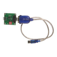
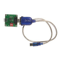
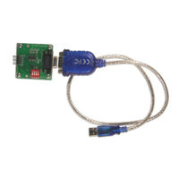
Fujitsu F2MC-16LX Series User Manual (14 pages)
PC Serial Programming Adapter Cable for Fujitsu Flash Microcontroller-F²MC-16LX/FR Family
Brand:
Fujitsu
| Category:
Computer Hardware
| Size: 0.15 MB
Share and save
Advertisement
Related Products
Fujitsu F2MCTM-16LX
Fujitsu F2MC-8L F202RA
Fujitsu F2MC-8L MB89202
Fujitsu F2 MC-8FX Family
Fujitsu F2MC-16FR
Fujitsu FMC-16LX/FR
Fujitsu FM3 family
Fujitsu FR Family FR60 Lite
Fujitsu FibreCAT TXF
Fujitsu SOFTUNE F2 MC-16
Fujitsu Categories
Air Conditioner
Laptop
Server
Scanner
Storage
More Fujitsu Manuals
Login
Sign In
OR
Sign in with Facebook
Sign in with Google
Upload manual
Upload from disk
Upload from URL