
Related Manuals for Motorola CMOS Logic


Summary of Contents for Motorola CMOS Logic
- Page 2 Master Index Product Selection Guide The “Better” Program B and UB Series Family Data CMOS Handling and Design Guidelines Data Sheets CMOS Reliability Equivalent Gate Count Packaging Information Including Surface Mounts...
- Page 3 This heading on a data sheet indicates that the device is in the formative stages or in design (under development). The disclaimer at the bottom of the first page reads: “This document contains information on a product under development. Motorola reserves the right to change or discontinue this product without notice.” Advance Information This heading on a data sheet indicates that the device is in sampling, preproduction, or first production stages.
- Page 4 DATA Prepared by Technical Information Center This book presents technical data for the broad line of CMOS logic integrated circuits and demonstrates Motorola’s continued commitment to Metal–Gate CMOS. Complete specifications are provided in the form of data sheets. In addi- tion, a Product Selector Guide and a Handling and Design Guidelines chapter have been included to familiarize the user with these circuits.
- Page 5 MOTOROLA CMOS LOGIC DATA...
- Page 6 Master Index...
- Page 7 MASTER INDEX This index includes Motorola’s entire MC14000 series CMOS products, although this book contains data sheets for Logic Devices only. Data sheets for devices in the CMOS/NMOS Special Functions Data book (DL130) are designated in the page number column as SF.
- Page 8 6–Channel A/D Converter Subsystem ....... . MOTOROLA CMOS LOGIC DATA CHAPTER 1...
- Page 9 ........6–307 CHAPTER 1 MOTOROLA CMOS LOGIC DATA 1–4...
- Page 10 ........6–494 MOTOROLA CMOS LOGIC DATA CHAPTER 1...
- Page 11 ..MC145453 33–Segment LCD Driver with Serial Interface ......CHAPTER 1 MOTOROLA CMOS LOGIC DATA 1–6...
- Page 12 Product Selection Guide...
- Page 13 ..........6–504 CHAPTER 2 MOTOROLA CMOS LOGIC DATA 2–2...
- Page 14 ......... 6–174 MOTOROLA CMOS LOGIC DATA CHAPTER 2...
- Page 15 MC14538B Dual Precision Monostable Multivibrator ......6–365 CHAPTER 2 MOTOROLA CMOS LOGIC DATA 2–4...
- Page 16 ........6–210 MC14568B Phase Comparator and Programmable Counters ....6–461 MOTOROLA CMOS LOGIC DATA CHAPTER 2 2–5...
- Page 17 The “Better” Program...
- Page 18 100% post burn–in functional and dc parametric tests at Motorola distributor or Motorola sales offices. “BETTER” 25 C (or max rated T A at Motorola’s option). Maximum pricing will be quoted as an adder to standard commercial PDA of 2% (functional) and 5% (DC and functional).
- Page 19 7. Special device specifications (48A’s) for logic products will 1. All standard 25 C dc and functional parameters will be reference 12MRM15301A as source of generic data for measured Go/No/Go at each readout. any customer required monthly audit reports. MOTOROLA CMOS LOGIC DATA CHAPTER 3 3–3...
- Page 20 B and UB Series Family Data...
- Page 21 Table 1 is in the industry format a 5.0 volt supply. Since the maximum allowable logic 0 for and Table 2 is in the equivalent Motorola format. The the second stage is 1.5 volts, this 0.5 volt output provides a Motorola format is used throughout this data book.
- Page 22 Î Î Î Î Î Î Î Î Î Î Î Î Î Î Î Î Î Î Î Î Î Î Î Î Î Î Î Î Î Î Î Î Î Î Î MOTOROLA CMOS LOGIC DATA CHAPTER 4 4–3...
- Page 23 * T LOW = – 55 _ C for Military temperature range device, – 40 C for Commercial temperature range device. T HIGH = + 125 _ C for Military temperature range device, + 85 _ C for Commercial temperature range device. #Applies for Worst Case input combinations. CHAPTER 4 MOTOROLA CMOS LOGIC DATA 4–4...
- Page 24 Î Î Î Î Î Î Î Î Î Î Î Î Î Î Î Î Î Î Î Î Î Î Î Î Î Î Î Î Î Î Î Î Î Î Table 2. Motorola Format for CMOS Industry B and UB Series Specifications Î...
- Page 25 CMOS Handling and Design Guidelines...
- Page 26 All MOS devices have insulated gates that are subject to This resistor helps limit accidental damage if the PC voltage breakdown. The gate oxide for Motorola CMOS de- board is removed and brought into contact with static vices is about 900 Å thick and breaks down at a gate–source generating materials.
- Page 27 = the board capacitance plus the driven device’s input capacitance in farads = 0.7 for propagation delay calculations = 2.3 for rise time calculations Figure 1. Networks for Minimizing ESD and Reducing CMOS Latch Up Susceptibility MOTOROLA CMOS LOGIC DATA CHAPTER 5 5–3...
- Page 28 I DD LATCH UP MODE SECONDARY BREAKDOWN LOW CURRENT JUNCTION AVALANCHE V DD V S = DATA SHEET MAXIMUM SUPPLY RATING Figure 3. Secondary Breakdown Characteristics CHAPTER 5 MOTOROLA CMOS LOGIC DATA 5–4...
- Page 29 Figure 7), the device may also go into oscillation from any noise in the system. Since CMOS devices dissipate the most power during switching, this oscillation can cause very large Figure 7. External Protection current drain and undesired switching. MOTOROLA CMOS LOGIC DATA CHAPTER 5 5–5...
- Page 30 This can be ac- 1 LSTTL load can be driven across the full temperature complished with the power supply filtering network or range. with a current–limiting regulator. CHAPTER 5 MOTOROLA CMOS LOGIC DATA 5–6...
- Page 31 P – WELL Figure 10. CMOS Wafer Cross Section N–CHANNEL OUTPUT N– N–SUBSTRATE RESISTANCE V DD V SS N– P– V DD P– V SS P–WELL RESISTANCE P–CHANNEL OUTPUT Figure 11. Latch Up Circuit Schematic MOTOROLA CMOS LOGIC DATA CHAPTER 5 5–7...
- Page 32 CMOS Handling and Design Guidelines...
- Page 33 All MOS devices have insulated gates that are subject to This resistor helps limit accidental damage if the PC voltage breakdown. The gate oxide for Motorola CMOS de- board is removed and brought into contact with static vices is about 900 Å thick and breaks down at a gate–source generating materials.
- Page 34 = the board capacitance plus the driven device’s input capacitance in farads = 0.7 for propagation delay calculations = 2.3 for rise time calculations Figure 1. Networks for Minimizing ESD and Reducing CMOS Latch Up Susceptibility MOTOROLA CMOS LOGIC DATA CHAPTER 5 5–3...
- Page 35 I DD LATCH UP MODE SECONDARY BREAKDOWN LOW CURRENT JUNCTION AVALANCHE V DD V S = DATA SHEET MAXIMUM SUPPLY RATING Figure 3. Secondary Breakdown Characteristics CHAPTER 5 MOTOROLA CMOS LOGIC DATA 5–4...
- Page 36 Figure 7), the device may also go into oscillation from any noise in the system. Since CMOS devices dissipate the most power during switching, this oscillation can cause very large Figure 7. External Protection current drain and undesired switching. MOTOROLA CMOS LOGIC DATA CHAPTER 5 5–5...
- Page 37 This can be ac- 1 LSTTL load can be driven across the full temperature complished with the power supply filtering network or range. with a current–limiting regulator. CHAPTER 5 MOTOROLA CMOS LOGIC DATA 5–6...
- Page 38 P – WELL Figure 10. CMOS Wafer Cross Section N–CHANNEL OUTPUT N– N–SUBSTRATE RESISTANCE V DD V SS N– P– V DD P– V SS P–WELL RESISTANCE P–CHANNEL OUTPUT Figure 11. Latch Up Circuit Schematic MOTOROLA CMOS LOGIC DATA CHAPTER 5 5–7...
- Page 39 Data Sheets...
- Page 40 IN 3 B IN 1 A IN 2 B IN 2 A IN 1 B IN 3 A OUT B OUT A OUT C V SS V SS IN 1 C NC = NO CONNECTION MC14000UB MOTOROLA CMOS LOGIC DATA 6–2...
- Page 41 (V in or V out ) V DD . Unused inputs must always be tied to an appropriate logic voltage level (e.g., either V SS or V DD ). Unused outputs must be left open. MOTOROLA CMOS LOGIC DATA MC14000UB 6–3...
- Page 42 5.0 Vdc I D = 10 Vdc V in , INPUT VOLTAGE (Vdc) V in , INPUT VOLTAGE (Vdc) Figure 2. Typical Voltage and Current Figure 3. Typical Voltage Transfer Transfer Characteristics Characteristics versus Temperature MC14000UB MOTOROLA CMOS LOGIC DATA 6–4...
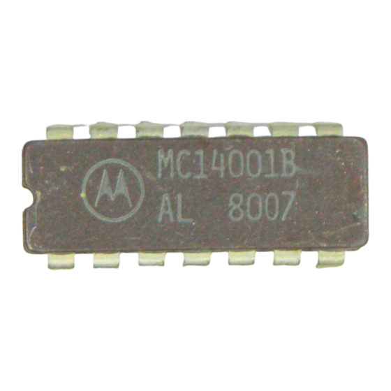
- Page 43 (V in or V out ) V DD . Unused inputs must always be tied to an appropriate logic voltage level (e.g., either V SS or V DD ). Unused outputs must be left open. MOTOROLA CMOS LOGIC DATA MC14001B 6–5...
- Page 44 NC = 6, 8 NC = 6, 8 MC14078B MC14068B 8–Input NOR Gate 8–Input NAND Gate V DD = PIN 14 V SS = PIN 7 FOR ALL DEVICES NC = 6, 8 NC = 6, 8 MC14001B MOTOROLA CMOS LOGIC DATA 6–6...
- Page 45 IN 3 B IN 1 B OUT C IN 4 A IN 2 B IN 2 B IN 2 C IN 1 B V SS IN 1 C V SS NC = NO CONNECTION MOTOROLA CMOS LOGIC DATA MC14001B 6–7...
- Page 46 I T is in µA (per package), C L in pF, V = (V DD – V SS ) in volts, f in kHz is input frequency, and k = 0.001 x the number of exercised gates per package. MC14001B MOTOROLA CMOS LOGIC DATA 6–8...
- Page 47 * All unused inputs of AND, NAND gates must be connected to V DD . t TLH t THL All unused inputs of OR, NOR gates must be connected to V SS . Figure 1. Switching Time Test Circuit and Waveforms MOTOROLA CMOS LOGIC DATA MC14001B 6–9...
- Page 48 5, 11 SAME AS 4, 12 ABOVE V SS * Inverter omitted in MC14002B V DD MC14078B Eight Input Gate V DD V SS SAME AS ABOVE SAME AS ABOVE SAME AS ABOVE V SS MC14001B MOTOROLA CMOS LOGIC DATA 6–10...
- Page 49 SAME AS 5, 11 ABOVE V DD V SS * Inverter omitted in MC14012B V SS SAME AS ABOVE V DD V SS V DD SAME AS ABOVE SAME AS ABOVE V SS V SS MOTOROLA CMOS LOGIC DATA MC14001B 6–11...
- Page 50 Figure 6. V GS = 15 Vdc Figure 7. V GS = – 15 Vdc These typical curves are not guarantees, but are design aids. Caution: The maximum rating for output current is 10 mA per pin. MC14001B MOTOROLA CMOS LOGIC DATA 6–12...
- Page 51 V DD V DD V DD V in V in V IL V IH V IL V IH V SS = 0 VOLTS DC (a) Inverting Function (b) Non–Inverting Function Figure 11. DC Noise Immunity MOTOROLA CMOS LOGIC DATA MC14001B 6–13...
- Page 52 (V in or V out ) V DD . Unused inputs must always be tied to an appropriate logic voltage level (e.g., either V SS or V DD ). Unused outputs must be left open. MC14001UB MOTOROLA CMOS LOGIC DATA 6–14...
- Page 53 Plastic “P and D/DW” Packages: – 7.0 mW/ _ C From 65 _ C To 125 _ C Ceramic “L” Packages: – 12 mW/ _ C From 100 _ C To 125 _ C MOTOROLA CMOS LOGIC DATA MC14001UB 6–15...
- Page 54 I T is in µH (per package), C L in pF, V = (V DD – V SS ) in volts, f in kHz is input frequency, and k = 0.001 x the number of exercised gates per package. MC14001UB MOTOROLA CMOS LOGIC DATA 6–16...
- Page 55 Figure 1. Switching Time Test Circuit and Waveforms MC14001UB CIRCUIT SCHEMATIC MC14002UB CIRCUIT SCHEMATIC (1/2 of Device Shown) V DD V DD 2, 9 3, 10 4, 11 5, 12 1, 13 V SS V SS MOTOROLA CMOS LOGIC DATA MC14001UB 6–17...
- Page 56 – 10 – 8.0 – 6.0 – 4.0 – 2.0 V DS , DRAIN VOLTAGE (Vdc) V DS , DRAIN VOLTAGE (Vdc) Figure 4. Typical Output Source Figure 5. Typical Output Sink Characteristics Characteristics MC14001UB MOTOROLA CMOS LOGIC DATA 6–18...
- Page 57 Input to output is A bidirectional low impedance when control input 1 is “low” and control input 2 is “high”. An open circuit when control input 1 is “high” and control input 2 is “low”. MOTOROLA CMOS LOGIC DATA MC14006B 6–19...
- Page 58 I T is in µA (per package), C L in pF, V = (V DD – V SS ) in volts, f in kHz is input frequency, and k = 0.001. PIN ASSIGNMENT D P1 V DD D P5 D P10 D P14 V SS NC = NO CONNECTION MC14006B MOTOROLA CMOS LOGIC DATA 6–20...
- Page 59 I OL D P14 D P14 EXTERNAL EXTERNAL V SS V SS POWER POWER SUPPLY SUPPLY Figure 1. Typical Output Source Current Figure 2. Typical Output Sink Current Characteristics Test Circuit Characteristics Test Circuit MOTOROLA CMOS LOGIC DATA MC14006B 6–21...
- Page 60 É É É É É É É É É É É É É É É É É É t TLH t THL É É É Output state can change since data previously clocked in might be in either state. É É É Figure 4. Switching Time Test Circuit and Waveforms MC14006B MOTOROLA CMOS LOGIC DATA 6–22...
- Page 61 Substrates of P–channel devices internally V DD = PIN 14 connected to V DD ; substrates of N–channel V SS = PIN 7 devices internally connected to V SS . Figure 1. Typical Application: 2–Input Analog Multiplexer MOTOROLA CMOS LOGIC DATA MC14007UB 6–23...
- Page 62 (V in or V out ) V DD . Unused inputs must always be tied to an appropriate logic voltage level (e.g., either V SS or V DD ). Unused outputs must be left open. MC14007UB MOTOROLA CMOS LOGIC DATA 6–24...
- Page 63 V DS , DRAIN VOLTAGE (Vdc) Figure 2. Typical Output Source Characteristics Figure 3. Typical Output Sink Characteristics These typical curves are not guarantees, but are design aids. Caution: The maximum current rating is 10 mA per pin. MOTOROLA CMOS LOGIC DATA MC14007UB 6–25...
- Page 64 Substrates of P–channel devices internally connected to V DD ; Substrates of N–channel devices internally connected to V SS . INPUT DISABLE OUTPUT Figure 6. AOI Functions Using Tree Logic OPEN X = Don’t Care Figure 5. 3–State Buffer MC14007UB MOTOROLA CMOS LOGIC DATA 6–26...
- Page 65 V DD B4 15 ADDER 13 S4 C out ADDER 12 S3 ADDER 11 S2 V SS C in ADDER 10 S1 V DD = PIN 16 C in V SS = PIN 8 MOTOROLA CMOS LOGIC DATA MC14008B 6–27...
- Page 66 (V in or V out ) V DD . Unused inputs must always be tied to an appropriate logic voltage level (e.g., either V SS or V DD ). Unused outputs must be left open. MC14008B MOTOROLA CMOS LOGIC DATA 6–28...
- Page 67 C in C out C in C out EXTERNAL EXTERNAL POWER POWER V SS V SS SUPPLY SUPPLY Figure 1. Typical Source Current Figure 2. Typical Sink Current Characteristics Test Circuit Characteristics Test Circuit MOTOROLA CMOS LOGIC DATA MC14008B 6–29...
- Page 68 V SS t PHL t PLH V OH S1 – S4 V OL t THL t TLH V OH C out V OL t PLH t PHL Figure 4. Switching Time Test Circuit and Waveforms MC14008B MOTOROLA CMOS LOGIC DATA 6–30...
- Page 69 C out C in Figure 5. Logic Diagram MOTOROLA CMOS LOGIC DATA MC14008B 6–31...
- Page 70 The guaranteed 16–bit adder speed at 10 V, 25 C, C L = 50 pF is: t p total = 290 + 310 + 300 = 900 ns Figure 6. Using the MC14008B in a 16–Bit Adder Configuration MC14008B MOTOROLA CMOS LOGIC DATA 6–32...
- Page 71 Ceramic “L” Packages: – 12 mW/ _ C From 100 _ C To 125 _ C TRUTH TABLE Inputs Outputs Clock † Data Reset V DD = PIN 14 V SS = PIN 7 Change X = Don’t Care † = Level Change MOTOROLA CMOS LOGIC DATA MC14013B 6–33...
- Page 72 (V in or V out ) V DD . Unused inputs must always be tied to an appropriate logic voltage level (e.g., either V SS or V DD ). Unused outputs must be left open. V SS MC14013B MOTOROLA CMOS LOGIC DATA 6–34...
- Page 73 #Data labelled “Typ” is not to be used for design purposes but is intended as an indication of the IC’s potential performance. ** Data must be valid for 250 ns with a 5 V supply, 100 ns with 10 V, and 70 ns with 15 V. LOGIC DIAGRAM (1/2 of Device Shown) MOTOROLA CMOS LOGIC DATA MC14013B 6–35...
- Page 74 (Data, Clock, and Output) (Set, Reset, Clock, and Output) TYPICAL APPLICATIONS n–STAGE SHIFT REGISTER n th CLOCK BINARY RIPPLE UP–COUNTER (Divide–by–2 n ) n th CLOCK T FLIP–FLOP MODIFIED RING COUNTER (Divide–by–(n+1)) n th CLOCK MC14013B MOTOROLA CMOS LOGIC DATA 6–36...
- Page 75 * Q6, Q7, & Q8 are available externally LOGIC DIAGRAM X = Don’t Care CLOCK V DD = PIN 16 P4 = PIN 4 V SS = PIN 8 P5 = PIN 13 MOTOROLA CMOS LOGIC DATA MC14014B MC14021B 6–37...
- Page 76 (V in or V out ) V DD . Unused inputs must always be tied to an appropriate logic voltage level (e.g., either V SS or V DD ). Unused outputs must be left open. V SS MC14014B MC14021B MOTOROLA CMOS LOGIC DATA 6–38...
- Page 77 I OH I OL EXTERNAL EXTERNAL POWER POWER SUPPLY SUPPLY Preset output under test to a logic “1” level. Figure 1. Output Source Current Test Circuit Figure 2. Output Sink Current Test Circuit MOTOROLA CMOS LOGIC DATA MC14014B MC14021B 6–39...
- Page 78 SWITCH POSITION 1 = PARALLEL IN V SS SWITCH POSITION 2 = SERIAL IN SW 2 t TLH t THL t WL = t WH = 50% DUTY CYCLE Figure 4. Switching Time Test Circuit and Waveforms MC14014B MC14021B MOTOROLA CMOS LOGIC DATA 6–40...
- Page 79 V SS = PIN 8 Q n–1 Q n–1 No Change No Change X = Don’t Care Q n = Q0, Q1, Q2, or Q3, as applicable. Q n–1 = Output of prior stage. MOTOROLA CMOS LOGIC DATA MC14015B 6–41...
- Page 80 Unused inputs must always be tied to an appropriate logic voltage Q1 A Q0 B level (e.g., either V SS or V DD ). Unused outputs must be left open. Q0 A Q1 B Q2 B Q3 A V SS MC14015B MOTOROLA CMOS LOGIC DATA 6–42...
- Page 81 #Data labelled “Typ” is not to be used for design purposes but is intended as an indication of the IC’s potential performance. V DD 0.01 µF PULSE 500 µF CERAMIC GENERATOR V DD PULSE GENERATOR V SS CLOCK DATA Figure 1. Power Dissipation Test Circuit and Waveform MOTOROLA CMOS LOGIC DATA MC14015B 6–43...
- Page 82 Figure 2. Switching Test Circuit and Waveforms V DD PULSE V DD CLOCK GENERATOR INPUT t su SYNC PULSE GENERATOR V DD DATA INPUT V SS Figure 3. Setup and Hold Time Test Circuit and Waveforms MC14015B MOTOROLA CMOS LOGIC DATA 6–44...
- Page 83 SINGLE BIT V DD RESET CLOCK DATA TO D OF NEXT BIT V SS DATA INPUT BUFFER RESET INPUT BUFFER CLOCK INPUT BUFFER V DD V DD V DD CLOCK RESET CLOCK DATA TO RESET DATA TO 4 BITS TO 4 BITS FIRST BIT V SS V SS...
- Page 84 NEXT BIT DATA RESET COMPLETE DEVICE DATA INPUT BUFFER CLOCK INPUT BUFFER RESET INPUT BUFFER DATA INPUT BUFFER CLOCK INPUT BUFFER V DD = PIN 16 V SS = PIN 8 RESET INPUT BUFFER MC14015B MOTOROLA CMOS LOGIC DATA 6–46...
- Page 85 Each MC14016B consists of four independent switches capable of controlling either digital or analog signals. The quad bilateral switch is used P SUFFIX PLASTIC in signal gating, chopper, modulator, demodulator and CMOS logic CASE 646 implementation. Diode Protection on All Inputs Supply Voltage Range = 3.0 Vdc to 18 Vdc...
- Page 86 V DD and switch input components. The reliability of the device will be unaffected unless the Maximum Ratings are exceeded. (See first page of this data sheet.) Reference Figure 14. MC14016B MOTOROLA CMOS LOGIC DATA 6–48...
- Page 87 #Data labelled “Typ” is not to be used for design purposes but is intended as an indication of the IC’s potential performance. PIN ASSIGNMENT IN 1 V DD OUT 1 CONTROL 1 OUT 2 CONTROL 4 IN 2 IN 4 CONTROL 2 OUT 4 CONTROL 3 OUT 3 V SS IN 3 MOTOROLA CMOS LOGIC DATA MC14016B 6–49...
- Page 88 – 10 – 8.0 – 4.0 V in , INPUT VOLTAGE (Vdc) V in , INPUT VOLTAGE (Vdc) Figure 4. V SS = – 5.0 V and – 7.5 V Figure 5. V SS = 0 V MC14016B MOTOROLA CMOS LOGIC DATA 6–50...
- Page 89 10 Vdc 5.0 Vdc QUAN–TECH MODEL V C = V DD 2283 OR EQUIV 1.0 k 10 k 100 k f, FREQUENCY (Hz) Figure 10. Noise Voltage Test Circuit Figure 11. Typical Noise Characteristics MOTOROLA CMOS LOGIC DATA MC14016B 6–51...
- Page 90 10 M 100 M f in , INPUT FREQUENCY (Hz) Figure 12. Typical Insertion Loss/Bandwidth Figure 13. Frequency Response Test Circuit Characteristics ON SWITCH CONTROL SECTION OF IC LOAD SOURCE Figure 14. ∆V Across Switch MC14016B MOTOROLA CMOS LOGIC DATA 6–52...
- Page 91 ANALOG SIGNAL EXTERNAL 0–TO–5 V DIGITAL CMOS DIGITAL CONTROL SIGNALS MC14016B CIRCUITRY Figure A. Application Example V DD V DD SWITCH SWITCH V SS V SS Figure B. External Germanium or Schottky Clipping Diodes MOTOROLA CMOS LOGIC DATA MC14016B 6–53...
- Page 92 X = Don’t Care. If n < 5 Carry = “1”, Otherwise = “0”. LOGIC DIAGRAM BLOCK DIAGRAM CLOCK CLOCK CLOCK CARRY ENABLE CLOCK ENABLE RESET RESET C out V DD = PIN 16 V SS = PIN 8 MC14017B MOTOROLA CMOS LOGIC DATA 6–54...
- Page 93 V DD . CLOCK Unused inputs must always be tied to an appropriate logic voltage level (e.g., either V SS or V DD ). Unused outputs must be left open. C out V SS MOTOROLA CMOS LOGIC DATA MC14017B 6–55...
- Page 94 * The formulas given are for the typical characteristics only at 25 _ C. #Data labelled “Typ” is not to be used for design purposes but is intended as an indication of the IC’s potential performance. MC14017B MOTOROLA CMOS LOGIC DATA 6–56...
- Page 95 CLOCK CLOCK MC14017B MC14017B MC14017B Q0 Q1 Q8 Q9 Q0Q1 Q8 Q9 Q8 Q9 8 DECODED 9 DECODED 8 DECODED OUTPUTS OUTPUTS OUTPUTS CLOCK FIRST STAGE INTERMEDIATE STAGES LAST STAGE Figure 3. Counter Expansion MOTOROLA CMOS LOGIC DATA MC14017B 6–57...
- Page 96 PLH V OH V OL t TLH t THL t PHL t PHL t PLH C out V OH V OL t THL t TLH Figure 4. AC Measurement Definition and Functional Waveforms MC14017B MOTOROLA CMOS LOGIC DATA 6–58...
- Page 97 JAM 5 Unused inputs must always be tied to an appropriate logic voltage level (e.g., either V SS or V DD ). Unused outputs must be left open. JAM 3 V SS JAM 4 MOTOROLA CMOS LOGIC DATA MC14018B 6–59...
- Page 98 I T (C L ) = I T (50 pF) + (C L – 50) Vfk where: I T is in µA (per package), C L in pF, V = (V DD – V SS ) in volts, f in kHz is input frequency, and k = 0.001. MC14018B MOTOROLA CMOS LOGIC DATA 6–60...
- Page 99 #Data labelled “Typ” is not to be used for design purposes but is intended as an indication of the IC’s potential performance. 20 ns 20 ns V DD ANY INPUT V SS t PLH t PHL V OH ANY OUTPUT V OL t TLH t THL Figure 1. Switching Time Waveforms MOTOROLA CMOS LOGIC DATA MC14018B 6–61...
- Page 100 JAM 3 JAM 4 JAM 5 Divide by 3 Q2 Q1 Skips all 1’s state CLOCK CLOCK 14 SHAPER DATA RESET 15 PRESET ENABLE 10 V DD = PIN 16 V SS = PIN 8 MC14018B MOTOROLA CMOS LOGIC DATA 6–62...
- Page 101 Q6 = PIN 4 Q9 = PIN 12 V DD = PIN 16 Q7 = PIN 6 Q10 = PIN 14 V SS = PIN 8 Q8 = PIN 13 Q11 = PIN 15 MOTOROLA CMOS LOGIC DATA MC14020B 6–63...
- Page 102 (V in or V out ) V DD . Unused inputs must always be tied to an appropriate logic voltage level (e.g., either V SS or V DD ). Unused outputs must be left open. V SS MC14020B MOTOROLA CMOS LOGIC DATA 6–64...
- Page 103 WH V DD t PLH t PHL CLOCK V SS 50% DUTY CYCLE t TLH t THL Figure 1. Power Dissipation Test Circuit Figure 2. Switching Time Test Circuit and Waveform and Waveforms MOTOROLA CMOS LOGIC DATA MC14020B 6–65...
- Page 104 1024 2048 4096 8192 16,384 CLOCK RESET Figure 3. Timing Diagram MC14020B MOTOROLA CMOS LOGIC DATA 6–66...
- Page 105 Otherwise = 0. BLOCK DIAGRAM CLOCK CLOCK CARRY CLOCK V DD ENABLE CLOCK ENABLE V SS RESET RESET C out V DD = PIN 16 V SS = PIN 8 NC = PIN 6, 9 MOTOROLA CMOS LOGIC DATA MC14022B 6–67...
- Page 106 Unused inputs must always be tied to an appropriate logic voltage level (e.g., either V SS or V DD ). Unused outputs must be left open. C out V SS NC = NO CONNECTION MC14022B MOTOROLA CMOS LOGIC DATA 6–68...
- Page 107 * The formulas given are for the typical characteristics only at 25 _ C. #Data labelled “Typ” is not to be used for design purposes but is intended as an indication of the IC’s potential performance. MOTOROLA CMOS LOGIC DATA MC14022B...
- Page 108 (except propagation delay). MC14022B MC14022B MC14022B Q0 Q1 Q6 Q7 Q0 Q1 Q6 Q7 Q6 Q7 6 DECODED 7 DECODED 6 DECODED OUTPUTS OUTPUTS OUTPUTS CLOCK FIRST STAGE INTERMEDIATE STAGES LAST STAGE Figure 3. Counter Expansion MC14022B MOTOROLA CMOS LOGIC DATA 6–70...
- Page 109 PHL V OH V OL t PLH t TLH t THL t PHL C out V OH t PHL V OL t THL t TLH Figure 4. AC Measurement Definition and Functional Waveforms MOTOROLA CMOS LOGIC DATA MC14022B 6–71...
- Page 110 Ceramic “L” Packages: – 12 mW/ _ C From 100 _ C To 125 _ C LOGIC DIAGRAM V SS CLOCK V DD = PIN 14 V SS = PIN 7 NC = NO CONNECTION RESET Q3 = PIN 9 Q4 = PIN 6 Q5 = PIN 5 MC14024B MOTOROLA CMOS LOGIC DATA 6–72...
- Page 111 (V in or V out ) V DD . Unused inputs must always be tied to an appropriate logic voltage level (e.g., either V SS or V DD ). Unused outputs must be left open. MOTOROLA CMOS LOGIC DATA MC14024B 6–73...
- Page 112 #Data labelled “Typ” is not to be used for design purposes but is intended as an indication of the IC’s potential performance. TRUTH TABLE Clock Reset State No Change All Outputs Low No Change All Outputs Low No Change All Outputs Low Advance One Count All Outputs Low MC14024B MOTOROLA CMOS LOGIC DATA 6–74...
- Page 113 Figure 1. Typical Output Source Figure 2. Typical Output Sink Characteristics Test Circuit Characteristics Test Circuit V DD 0.01 µF 500 µF CERAMIC PULSE GENERATOR R Q7 V SS Figure 3. Power Dissipation Test Circuit MOTOROLA CMOS LOGIC DATA MC14024B 6–75...
- Page 114 t WL t WH V DD CLOCK (1) V SS t rem RESET (2) V DD V SS t PLH1 t PHL1 t R1 V OH Q1 (12) V OL t TLH t R2 t PHL2 t THL t PLH2 V OH V OL Q2 (11)
- Page 115 (V in or V out ) V DD . Unused inputs must always be tied to an appropriate logic voltage level (e.g., either V SS or V DD ). Unused outputs must be left open. MOTOROLA CMOS LOGIC DATA MC14027B 6–77...
- Page 116 I T is in µA (per package), C L in pF, V = (V DD – V SS ) in volts, f in kHz is input frequency, and k = 0.002. PIN ASSIGNMENT V DD V SS MC14027B MOTOROLA CMOS LOGIC DATA 6–78...
- Page 117 * The formulas given are for the typical characteristics only at 25 _ C. #Data labelled “Typ” is not to be used for design purposes but is intended as an indication of the IC’s potential performance. MOTOROLA CMOS LOGIC DATA MC14027B...
- Page 118 Inputs J and K are kept high. V OL Figure 1. Dynamic Signal Waveforms Figure 2. Dynamic Signal Waveforms (J, K, Clock, and Output) (Set, Reset, Clock, and Output) LOGIC DIAGRAM (1/2 of Device Shown) MC14027B MOTOROLA CMOS LOGIC DATA 6–80...
- Page 119 D C B A Q9 Q8 Q7 Q6 Q5 Q4 Q3 Q2 Q1 Q0 BLOCK DIAGRAM 3–BIT OCTAL BINARY 8421 DECODED INPUTS DECIMAL OUTPUTS DECODED INPUTS OUTPUTS V DD = PIN 16 V SS = PIN 8 MOTOROLA CMOS LOGIC DATA MC14028B 6–81...
- Page 120 (V in or V out ) V DD . Unused inputs must always be tied to an appropriate logic voltage level (e.g., either V SS or V DD ). Unused outputs must be left open. V SS MC14028B MOTOROLA CMOS LOGIC DATA 6–82...
- Page 121 20 ns 20 ns V DD INPUT C V SS Inputs A, B, and D low. t PLH t PHL V OH V OL t TLH t THL Figure 1. Dynamic Signal Waveforms MOTOROLA CMOS LOGIC DATA MC14028B 6–83...
- Page 122 The MC14028B can be used in decimal digit displays, such as, neon readouts or incandescent projection indicators Figure 2. Code Conversion Circuit and Truth Table as shown in Figure 4. Code and Redefined Output Numbers Hexadecimal Decimal Inputs Output Numbers MC14028B MOTOROLA CMOS LOGIC DATA 6–84...
- Page 123 MC14028B MC14028B MC14028B MC14028B MC14028B *1/6 MC14069UB 64 OUTPUTS (SELECTED OUTPUT IS HIGH) Figure 3. Six–Bit Binary 1–of–64 Decoder APPROPRIATE APPROPRIATE VOLTAGE VOLTAGE NEON INCANDESCENT DISPLAY DISPLAY MC14028B Figure 4. Decimal Digit Display Application MOTOROLA CMOS LOGIC DATA MC14028B 6–85...
- Page 124 Ceramic “L” Packages: – 12 mW/ _ C From 100 _ C To 125 _ C TRUTH TABLE Preset Enable Carry In Up/Down Action No Count Count Up Count Down Preset X = Don’t Care MC14029B MOTOROLA CMOS LOGIC DATA 6–86...
- Page 125 (V in or V out ) V DD . Unused inputs must always be tied to an appropriate logic voltage level (e.g., either V SS or V DD ). Unused outputs must be left open. MOTOROLA CMOS LOGIC DATA MC14029B 6–87...
- Page 126 * The formulas given are for the typical characteristics only at 25 _ C. #Data labelled “Typ” is not to be used for design purposes but is intended as an indication of the IC’s potential performance. MC14029B MOTOROLA CMOS LOGIC DATA 6–88...
- Page 127 PRESET ENABLE V SS 20 ns t TLH C out ONLY V OH Q0 OR CARRY OUT V OL t PLH t THL t PHL t PLH Figure 2. Switching Time Test Circuit and Waveforms MOTOROLA CMOS LOGIC DATA MC14029B 6–89...
- Page 128 C out 2 C out 3 (MSD) COUNT * t W 900 ns @ V DD = 5 V Figure 3. Divide by N BCD Down Counter and Timing Diagram (Shown for N = 123) MC14029B MOTOROLA CMOS LOGIC DATA 6–90...
- Page 129 BINARY/DECADE PRESET ENABLE CARRY IN CARRY OUT UP/DOWN CLOCK...
- Page 130 (e.g., either V SS or V DD ). Unused outputs must be left open. CLOCK 3 CARRY RESET 6 LOGIC DIAGRAMS MC14032B MC14038B (ONE SECTION AND COMMON INPUTS SHOWN) INVERT INVERT CARRY CARRY RESET RESET NEXT NEXT CLOCK CLOCK STAGE STAGE MC14032B MC14038B MOTOROLA CMOS LOGIC DATA 6–92...
- Page 131 I T is in µA (per package), C L in pF, V = (V DD – V SS ) in volts, f in kHz is input frequency, and k = 0.003. PIN ASSIGNMENT V DD INV 3 INV 2 CARRY RESET INV 1 V SS MOTOROLA CMOS LOGIC DATA MC14032B MC14038B 6–93...
- Page 132 + 49 0.1101110 = + 110 1.0101001 = – 87 1.0010000 = – 112 0.1010101 = + 85 NOTE: Unused input pins must be connected to either V DD or V SS . MC14032B MC14038B MOTOROLA CMOS LOGIC DATA 6–94...
- Page 133 20 ns INV1 V DD PROGRAMMABLE CLOCK PULSE INV2 V SS VARIABLE GENERATOR WIDTH V DD INV3 CLOCK V SS t THL t TLH V SS Figure 3. Power Dissipation Test Circuit and Waveforms MOTOROLA CMOS LOGIC DATA MC14032B MC14038B 6–95...
- Page 134 V SS t su CLOCK V DD V SS t PHL t PLH t PHL t PLH V OH V OL t THL t TLH Figure 4. Switching Time Test Circuit and Waveforms MC14032B MC14038B MOTOROLA CMOS LOGIC DATA 6–96...
- Page 135 (V in or V out ) V DD . Unused inputs must always be tied to an appropriate logic voltage level (e.g., either V SS or V DD ). Unused outputs must be left open. MOTOROLA CMOS LOGIC DATA MC14034B 6–97...
- Page 136 I T (C L ) = I T (50 pF) + (C L – 50) Vfk where: I T is in µA (per package), C L in pF, V = (V DD – V SS ) in volts, f in kHz is input frequency, and k = 0.004. MC14034B MOTOROLA CMOS LOGIC DATA 6–98...
- Page 137 †Outputs change at positive transition of clock in the serial mode and when the A/S input is low in the parallel mode. During transfer from parallel to serial operation, A/S should remain low in order to prevent D S transfer into flip–flops. MOTOROLA CMOS LOGIC DATA MC14034B...
- Page 138 V DD V DD A ENABLE FLIP– FLOP A/B 11 *D FLIP FLOP 6 STAGES SERIAL DATA 10 (SAME AS C M C S STAGE 1) PARALLEL SERIAL 13 V DD ASYN/SYN 14 CLOCK 15 MC14034B MOTOROLA CMOS LOGIC DATA 6–100...
- Page 139 B1 B2 B3 B4 B5 B6 B7 B8 V SS V SS Figure 2. A Synchronous Data Input, B Parallel Figure 3. B Synchronous Data Input, A Parallel Data Output and Setup Time Data Output and Setup Time MOTOROLA CMOS LOGIC DATA MC14034B 6–101...
- Page 140 C B1 B2 B3 B4 B5 B6 B7 B8 B2 B3 B4 B5 B6 B7 B8 SERIAL DATA CLOCK Figure 5. 16–Bit Parallel In/Parallel Out, Parallel In/Serial Out, Serial In/Parallel Out, Serial In/Serial Out Register MC14034B MOTOROLA CMOS LOGIC DATA 6–102...
- Page 141 3 and 4 for parallel loading. When parallel inputs are not used, Reg. 3 and 4 and associated logic are not required. *Shift left input must be disabled during parallel entry. Figure 6. Shift Right/Shift Left with Parallel Inputs MOTOROLA CMOS LOGIC DATA MC14034B 6–103...
- Page 142 Output t n Output Q0 (n – 1) Q0 (n – 1) X = Don’t Care P/S = 0 = Serial Mode Q0 (n – 1) T/C = 1 = True Outputs MC14035B MOTOROLA CMOS LOGIC DATA 6–104...
- Page 143 (V in or V out ) V DD . Unused inputs must always be tied to an appropriate logic voltage level (e.g., either V SS or V DD ). Unused outputs must be left open. MOTOROLA CMOS LOGIC DATA MC14035B 6–105...
- Page 144 1/f cl J–K INPUT t su t su t su INPUT D P0 INPUT t THL t su t TLH T/C INPUT LOW t PHL t PLH t PHL t PLH Figure 1. Timing Diagram MC14035B MOTOROLA CMOS LOGIC DATA 6–106...
- Page 145 SERIAL OUTPUT LEFT SHIFT SERIAL INPUT RIGHT SHIFT V DD SERIAL OUTPUT V DD D P3 D P2 D P1 D P0 V SS V DD RIGHT SHIFT SERIAL INPUT RESET CLOCK LEFT/RIGHT SHIFT SELECT MOTOROLA CMOS LOGIC DATA MC14035B 6–107...
- Page 146 Q4 = PIN 5 Q7 = PIN 4 V DD = PIN 16 Q5 = PIN 3 Q8 = PIN 13 V SS = PIN 8 Q6 = PIN 2 Q9 = PIN 12 MC14040B MOTOROLA CMOS LOGIC DATA 6–108...
- Page 147 (V in or V out ) V DD . Unused inputs must always be tied to an appropriate logic voltage level (e.g., either V SS or V DD ). Unused outputs must be left open. V SS MOTOROLA CMOS LOGIC DATA MC14040B 6–109...
- Page 148 WH V DD t PLH t PHL CLOCK V SS 50% DUTY CYCLE t TLH t THL Figure 1. Power Dissipation Test Circuit Figure 2. Switching Time Test Circuit and Waveform and Waveforms MC14040B MOTOROLA CMOS LOGIC DATA 6–110...
- Page 149 MC14040B. By selecting er. The resulting output frequency is 1.0 pulse/minute. V DD MC14040B 1.0 M 1.0 PULSE/MINUTE OUTPUT 20 pF 120 Vac MC14012B MC14012B 60 Hz V SS MOTOROLA CMOS LOGIC DATA MC14040B 6–111...
- Page 150 Ceramic “L” Packages: – 12 mW/ _ C From 100 _ C To 125 _ C LOGIC DIAGRAM TRUTH TABLE LATCH Clock Polarity CLOCK Data POLARITY Latch Data Latch LATCH LATCH V DD = PIN 16 V SS = PIN 8 LATCH MC14042B MOTOROLA CMOS LOGIC DATA 6–112...
- Page 151 (V in or V out ) V DD . Unused inputs must always be tied to an appropriate logic voltage level (e.g., either V SS or V DD ). Unused outputs must be left open. MOTOROLA CMOS LOGIC DATA MC14042B 6–113...
- Page 152 Q OUTPUT V SS For Power Dissipation test, each output t THL t TLH is loaded with capacitance C L . Figure 1. AC and Power Dissipation Test Circuit and Timing Diagram (Data to Output) MC14042B MOTOROLA CMOS LOGIC DATA 6–114...
- Page 153 DATA INPUT t su P.G. 2 t PLH Q OUTPUT * Input clock rise time is 20 ns except for maximum rise time test. Figure 2. AC Test Circuit and Timing Diagram (Clock to Output) MOTOROLA CMOS LOGIC DATA MC14042B 6–115...
- Page 154 TRUTH TABLE TRUTH TABLE S R E S R E X X 0 High X X 0 High Impedance Impedance No Change No Change ENABLE ENABLE X = Don’t Care X = Don’t Care MC14043B MC14044B MOTOROLA CMOS LOGIC DATA 6–116...
- Page 155 †Temperature Derating: Plastic “P and D/DW” Packages: – 7.0 mW/ _ C From 65 _ C To 125 _ C Ceramic “L” Packages – 12 mW/ _ C From 100 _ C To 125 _ C MOTOROLA CMOS LOGIC DATA MC14043B MC14044B...
- Page 156 V DD V DD RESET RESET V SS V SS t THL t TLH t TLH t THL V OH V OH V OL V OL t PLH t PHL t PLH t PHL MC14043B MC14044B MOTOROLA CMOS LOGIC DATA 6–118...
- Page 157 V SS t PZH V DD V OL t PHZ t PZL t PLZ V OH V SS PIN ASSIGNMENT MC14043B MC14044B V DD V DD V SS V SS NC = NO CONNECTION MOTOROLA CMOS LOGIC DATA MC14043B MC14044B 6–119...
- Page 158 VCO in 11 R1 CONTROLLED 12 R2 OSCILLATOR V DD = PIN 16 6 C1 A (VCO) 7 C1 B V SS = PIN 8 SOURCE FOLLOWER 10 SF out V SS 15 ZENER MC14046B MOTOROLA CMOS LOGIC DATA 6–120...
- Page 159 I T in µA, C L in pF, VCO in , V DD in Vdc, f in kHz, and 1 x 10 –1 V DD 2 + I Q R1, R2, R SF in MΩ, C L on VCO out . MOTOROLA CMOS LOGIC DATA MC14046B 6–121...
- Page 160 Î Î Î Î Î Î Î Î Î Î Î Î Î Î Î Î Î Î Î Î Î Î Î Î * The formula given is for the typical characteristics only. MC14046B MOTOROLA CMOS LOGIC DATA 6–122...
- Page 161 Î Î Î Î Î Î Î Î Î Î Î Î Î Î Î Î Î Î Î Î Î Î Î Î Î Î Î Î Î Î Î Î Î Î Î Figure 2. Design Information MOTOROLA CMOS LOGIC DATA MC14046B 6–123...
- Page 162 (2) G. S. Moschytz, “Miniature RC Filters Using Phase–Locked Loop”, BSTJ, May, 1965. (3) Garth Nash, “Phase–Lock Loop Design Fundamentals”, AN–535, Motorola Inc. (4) A. B. Przedpelski, “Phase–Locked Loop Design Articles”, AR254, reprinted by Motorola Inc. Figure 3. General Phase–Locked Loop Connections and Waveforms...
- Page 163 LOGIC DIAGRAM MC14049B MC14050B NC = PIN 13, 16 NC = PIN 13, 16 V SS = PIN 8 V SS = PIN 8 V DD = PIN 1 V DD = PIN 1 MOTOROLA CMOS LOGIC DATA MC14049B MC14050B 6–125...
- Page 164 18 V and V SS V out V DD are recommended. Unused inputs must always be tied to an appropriate logic voltage level (e.g., either V SS or V DD ). Unused outputs must be left open. MC14049B MC14050B MOTOROLA CMOS LOGIC DATA 6–126...
- Page 165 – 10 – 8.0 – 6.0 – 4.0 – 2.0 V DS , DRAIN–TO–SOURCE VOLTAGE (Vdc) V DS , DRAIN–TO–SOURCE VOLTAGE (Vdc) Figure 1. Typical Output Source Characteristics Figure 2. Typical Output Sink Characteristics MOTOROLA CMOS LOGIC DATA MC14049B MC14050B 6–127...
- Page 166 THL t TLH V SS t PHL t PHL V OH OUTPUT MC14050B # Invert on MC14049B only V OL t TLH t THL Figure 4. Switching Time Test Circuit and Waveforms MC14049B MC14050B MOTOROLA CMOS LOGIC DATA 6–128...
- Page 167 Î Î Î †Temperature Derating: All Packages: See Figure 4. CIRCUIT SCHEMATIC (1/6 OF CIRCUIT SHOWN) NC = PIN 13, 16 V SS = PIN 8 MC14049UB V DD = PIN 1 V DD V SS MOTOROLA CMOS LOGIC DATA MC14049UB 6–129...
- Page 168 I T (C L ) = I T (50 pF) + (C L – 50) Vfk where: I T is in µA (per package), C L in pF, V = (V DD – V SS ) in volts, f in kHz is input frequency, and k = 0.002. MC14049UB MOTOROLA CMOS LOGIC DATA 6–130...
- Page 169 V DD = 15 Vdc V DD = 10 Vdc – 55 C V DD = 5 Vdc +125 C V in , INPUT VOLTAGE (Vdc) Figure 1. Typical Voltage Transfer Characteristics versus Temperature MOTOROLA CMOS LOGIC DATA MC14049UB 6–131...
- Page 170 (e.g., either V SS or V DD ). Unused outputs must be left open. IN B OUT E OUT C IN E IN C OUT D V SS IN D NC = NO CONNECTION MC14049UB MOTOROLA CMOS LOGIC DATA 6–132...
- Page 171 V EE = PIN 7 V EE = PIN 7 Note: Control Inputs referenced to V SS , Analog Inputs and Outputs reference to V EE . V EE must be V SS . MOTOROLA CMOS LOGIC DATA MC14051B MC14052B MC14053B 6–133...
- Page 172 V DD and switch input components. The reliability of the device will be unaffected unless the Maximum Ratings are exceeded. (See first page of this data sheet.) MC14051B MC14052B MC14053B MOTOROLA CMOS LOGIC DATA 6–134...
- Page 173 V DD . Unused inputs must always be tied to an appropriate logic voltage level (e.g., either V SS , V EE , or V DD ). Unused outputs must be left open. MOTOROLA CMOS LOGIC DATA MC14051B MC14052B MC14053B 6–135...
- Page 174 X3 11 X1 13 Y0 1 Y0 2 15 Y Y1 5 Y1 1 Y2 2 Z0 5 Y3 4 Z1 3 Figure 3. MC14052B Functional Diagram Figure 4. MC14053B Functional Diagram MC14051B MC14052B MC14053B MOTOROLA CMOS LOGIC DATA 6–136...
- Page 175 C L = 50 pF V EE COMMON V DD Figure 9. Crosstalk, Control Input to Figure 10. Off Channel Leakage Common O/I NOTE: See also Figures 7 and 8 on Page 6–51. MOTOROLA CMOS LOGIC DATA MC14051B MC14052B MC14053B 6–137...
- Page 176 Figure 15. Comparison at 25 C, V DD = – V EE PIN ASSIGMENT MC14051B MC14052B MC14053B V DD V DD V DD V EE V EE V EE V SS V SS V SS MC14051B MC14052B MC14053B MOTOROLA CMOS LOGIC DATA 6–138...
- Page 177 + 10 to – 5 = 15 V p–p Î Î Î Î Î Î Î Î Î Î Î Î Î Î Î Î Î Î Î Î Î Î Î Î Î Î Î Î Î MOTOROLA CMOS LOGIC DATA MC14051B MC14052B MC14053B 6–139...
- Page 178 OUT 1 CLOCK RESET Q6 = PIN 4 Q8 = PIN 14 Q10 = PIN 15 V DD = PIN 16 Q7 = PIN 6 Q9 = PIN 13 V SS = PIN 8 MC14060B MOTOROLA CMOS LOGIC DATA 6–140...
- Page 179 # Data labelled “Typ” is not to be used for design purposes but is intended as an indication of the IC’s potential performance. ** The formulas given are for the typical characteristics only at 25 _ C. MOTOROLA CMOS LOGIC DATA MC14060B...
- Page 180 20 ns t PLH t PHL V DD CLOCK V SS t TLH t THL 50% DUTY CYCLE Figure 1. Power Dissipation Test Circuit Figure 2. Switching Time Test Circuit and Waveform and Waveforms MC14060B MOTOROLA CMOS LOGIC DATA 6–142...
- Page 181 Î Î Î Î Î Î Î Î Î Î Î Î Î Î Î Î Î Î Î * Complete oscillator includes crystal, capacitors, and resistors. Figure 7. Typical Data for Crystal Oscillatgor Circuit MOTOROLA CMOS LOGIC DATA MC14060B 6–143...
- Page 182 CERAMIC CASE 632 The MC14066B consists of four independent switches capable of controlling either digital or analog signals. This quad bilateral switch is useful in signal gating, chopper, modulator, demodulator and CMOS logic implementation. P SUFFIX PLASTIC The MC14066B is designed to be pin–for–pin compatible with the CASE 646 MC14016B, but has much lower ON resistance.
- Page 183 V DD and switch input components. The reliability of the device will be unaffected unless the Maximum Ratings are exceeded. (See first page of this data sheet.) MOTOROLA CMOS LOGIC DATA MC14066B...
- Page 184 Unused inputs must always be tied to an appropriate logic voltage level (e.g., either V SS or V DD ). Unused outputs must be left open. IN 2 IN 4 CONTROL 2 OUT 4 CONTROL 3 OUT 3 V SS IN 3 MC14066B MOTOROLA CMOS LOGIC DATA 6–146...
- Page 185 C L = 50 pF SECTION OF IC 10 k V SS V DD V C = – 5.0 V TO + 5.0 V SWING Figure 5. Crosstalk, Figure 6. Off Channel Leakage Control to Output MOTOROLA CMOS LOGIC DATA MC14066B 6–147...
- Page 186 V in , INPUT VOLTAGE (VOLTS) V in , INPUT VOLTAGE (VOLTS) Figure 11. Comparison at 25 C, V DD = – V SS Figure 10. V DD = 2.5 V, V SS = – 2.5 V MC14066B MOTOROLA CMOS LOGIC DATA 6–148...
- Page 187 + 5 V EXTERNAL 0–TO–5 V DIGITAL MC14066B CMOS CONTROL SIGNALS DIGITAL CIRCUITRY Figure A. Application Example V DD V DD SWITCH SWITCH V SS V SS Figure B. External Germanium or Schottky Clipping Diodes MOTOROLA CMOS LOGIC DATA MC14066B 6–149...
- Page 188 Pin for Pin Replacement for CD4067B and CD4097B MC14067B MC14097B 16–Channel Analog Dual 8–Channel Analog Multiplexer/Demultiplexer Multiplexer/Demultiplexer INHIBIT INHIBIT CONTROLS CONTROLS COMMON OUT/IN SWITCHES COMMONS SWITCHES IN/OUT OUT/IN IN/OUT V DD = PIN 24 V SS = PIN 12 MC14067B MC14097B MOTOROLA CMOS LOGIC DATA 6–150...
- Page 189 Selected Selected Selected Channel Channels None None X = Don’t Care MC14067 FUNCTIONAL DIAGRAM MC14097 FUNCTIONAL DIAGRAM INHIBIT INHIBIT CONTROL CONTROL 1–OF–16 DECODER 1–OF–8 DECODER INPUTS INPUTS IN/OUT OUT/IN IN/OUT OUT/IN IN/OUT OUT/IN MOTOROLA CMOS LOGIC DATA MC14067B MC14097B 6–151...
- Page 190 V DD and switch input components. The reliability of the device will be unaffected unless the Maximum Ratings are exceeded. (See first page of this data sheet.) MC14067B MC14097B MOTOROLA CMOS LOGIC DATA 6–152...
- Page 191 Î Î Î Î Î Î Î Î Î Î Î #Data labelled “Typ” is not to be used for design purposes but is intended as an indication of the IC’s potential performance. MOTOROLA CMOS LOGIC DATA MC14067B MC14097B 6–153...
- Page 192 V DD SOURCE V SS V DD Figure 1. ∆V Across Switch Figure 2. Off Channel Leakage MC14067B MC14097B PIN ASSIGNMENT PIN ASSIGNMENT V DD V DD INHIBIT V SS INHIBIT V SS MC14067B MC14097B MOTOROLA CMOS LOGIC DATA 6–154...
- Page 193 V in V in Figure 5. Bandwidth and Off–Channel Figure 6. Channel Separation Feedthrough Attenuation (Adjacent Channels Used for Setup) V out C L = 50 pF Figure 7. Crosstalk, Control to Common O/I MOTOROLA CMOS LOGIC DATA MC14067B MC14097B 6–155...
- Page 194 V in , INPUT VOLTAGE (VOLTS) V in , INPUT VOLTAGE (VOLTS) Figure 12. V DD = 2.5 V, V SS = – 2.5 V Figure 13. Comparison at 25 C, V DD = – V SS MC14067B MC14097B MOTOROLA CMOS LOGIC DATA 6–156...
- Page 195 MC14067B EXTERNAL MC14097B 0–TO–5 V DIGITAL CMOS CONTROL SIGNALS DIGITAL CIRCUITRY Figure A. Application Example V DD V DD SWITCH COMMON V SS V SS Figure B. External Germanium or Schottky Clipping Diodes MOTOROLA CMOS LOGIC DATA MC14067B MC14097B 6–157...
- Page 196 V DD V DD OUTPUT INPUT PULSE V SS GENERATOR INPUT t PHL t PLH V OH V SS OUTPUT V OL t THL t TLH Figure 1. Switching Time Test Circuit and Waveforms MC14069UB MOTOROLA CMOS LOGIC DATA 6–158...
- Page 197 (V in or V out ) V DD . Unused inputs must always be tied to an appropriate logic voltage level (e.g., either V SS or V DD ). Unused outputs must be left open. MOTOROLA CMOS LOGIC DATA MC14069UB 6–159...
- Page 198 * Inverted output on MC14077B only. IN 2 B IN 2 C #Connect unused input to V DD for MC14070B, to V SS for MC14077B. V SS IN 1 C Figure 2. Switching Time Test Circuit and Waveforms MC14070B MC14077B MOTOROLA CMOS LOGIC DATA 6–160...
- Page 199 (V in or V out ) V DD . Unused inputs must always be tied to an appropriate logic voltage level (e.g., either V SS or V DD ). Unused outputs must be left open. MOTOROLA CMOS LOGIC DATA MC14070B MC14077B 6–161...
- Page 200 Clock When either output disable A or B (or both) is (are) high the output is disabled to the high–impedance state; however sequential operation of the flip–flops is not affected. X = Don’t Care. MC14076B MOTOROLA CMOS LOGIC DATA 6–162...
- Page 201 I T (C L ) = I T (50 pF) + (C L – 50) Vfk where: I T is in µA (per package), C L in pF, V = (V DD – V SS ) in volts, f in kHz is input frequency, and k = 0.002. MOTOROLA CMOS LOGIC DATA MC14076B...
- Page 202 (V in or V out ) V DD . Unused inputs must always be tied to an appropriate logic voltage level (e.g., either V SS or V DD ). Unused outputs must be left open. MC14076B MOTOROLA CMOS LOGIC DATA 6–164...
- Page 203 OUTPUT DISABLE A OUTPUT OUTPUT DISABLE B DISABLE 3 Q0 DATA DISABLE A DATA DISABLE B DATA DISABLE V SS D1 13 4 Q1 CLOCK D2 12 5 Q2 D3 11 6 Q3 RESET 15 MOTOROLA CMOS LOGIC DATA MC14076B 6–165...
- Page 204 (V in or V out ) V DD . Unused inputs must always be tied to an appropriate logic voltage level (e.g., either V SS or V DD ). Unused outputs must be left open. MC14093B MOTOROLA CMOS LOGIC DATA 6–166...
- Page 205 I T (C L ) = I T (50 pF) + (C L – 50) Vfk where: I T is in µA (per package), C L in pF, V = (V DD – V SS ) in volts, f in kHz is input frequency, and k = 0.004. MOTOROLA CMOS LOGIC DATA MC14093B...
- Page 206 V SS V SS (a) Schmitt Triggers will square up (b) A Schmitt trigger offers maximum inputs with slow rise and fall times. noise immunity in gate applications. Figure 2. Typical Schmitt Trigger Applications MC14093B MOTOROLA CMOS LOGIC DATA 6–168...
- Page 207 OUT D IN 1 B OUT C IN 2 B IN 2 C V SS IN 1C V T– V T+ V DD V in , INPUT VOLTAGE (Vdc) Figure 5. Typical Transfer Characteristics MOTOROLA CMOS LOGIC DATA MC14093B 6–169...
- Page 208 No Chg. No Chg. No Chg. Z = High Impedance X = Don’t Care * At the positive clock edge, information in the 7th shift register stage is transferred to Q8 and Q S . MC14094B MOTOROLA CMOS LOGIC DATA 6–170...
- Page 209 I T (C L ) = I T (50 pF) + (C L – 50) Vfk where: I T is in µA (per package), C L in pF, V = (V DD – V SS ) in volts, f in kHz is input frequency, and k = 0.001. MOTOROLA CMOS LOGIC DATA MC14094B...
- Page 210 #Data labelled “Typ” is not to be used for design purposes but is intended as an indication of the IC’s potential performance. 3–STATE TEST CIRCUIT FOR t PHZ AND t PZH FOR t PLZ AND t PZL V SS V DD O.E. DATA OUTPUT 50 pF CLOCK MC14094B MOTOROLA CMOS LOGIC DATA 6–172...
- Page 211 DATA IN t WL STROBE OUTPUT ENABLE t PLH t PLH t PZH t PLZ t PZL t PHZ t PHL ³ t PHL t TLH t THL t PLH t PLH t PHL MOTOROLA CMOS LOGIC DATA MC14094B 6–173...
- Page 212 DISABLE Unused inputs must always be tied to an appropriate logic voltage level (e.g., either V SS or V DD ). Unused outputs must be left open. WRITE/ V SS V SS READ MC14099B MC14599B MOTOROLA CMOS LOGIC DATA 6–174...
- Page 213 I T (C L ) = I T (50 pF) + (C L – 50) Vfk where: I T is in µA (per package), C L in pF, V = (V DD – V SS ) in volts, f in kHz is input frequency, and k = 0.004. MOTOROLA CMOS LOGIC DATA MC14099B MC14599B...
- Page 214 Î Î Î Î Î Î Î Î Î Î Î #Data labelled “Typ” is not to be used for design purposes but is intended as an indication of the IC’s potential performance. MC14099B MC14599B MOTOROLA CMOS LOGIC DATA 6–176...
- Page 215 V DD WRITE t TLH t THL DISABLE V SS t w(H) t su V DD V DD RESET DATA V SS V SS t PHL OUTPUT Q MOTOROLA CMOS LOGIC DATA MC14099B MC14599B 6–177...
- Page 216 Z = High impedance. Q n = State of addressed latch. CAUTION: To avoid unintentional data changes in the latches, Write Disable must be active (high) during transitions on the address inputs A0, A1, and A2. MC14099B MC14599B MOTOROLA CMOS LOGIC DATA 6–178...
- Page 217 Ç Ç Ç Ç Ç Ç Ç DATA V SS Ç Ç Ç Ç Ç Ç Ç t PLH , t PHL V DD A2, A1, A0 V SS NOTE: 1. Invalid Data Output 2. Reset in LOW State MOTOROLA CMOS LOGIC DATA MC14099B MC14599B 6–179...
- Page 218 (V in or V out ) V DD . Unused inputs must always be tied to an appropriate logic voltage level (e.g., either V SS or V DD ). Unused outputs must be left open. MC14106B MOTOROLA CMOS LOGIC DATA 6–180...
- Page 219 I T is in µA (per package), C L in pF, V = (V DD – V SS ) in volts, f in kHz is input frequency, and k = 0.001. †V H = V T+ – V T– (But maximum variation of V H is specified as less that V T+ max – V T– min ). MOTOROLA CMOS LOGIC DATA MC14106B...
- Page 220 V out V out V SS V SS (a) Schmitt Triggers will square up (b) A Schmitt trigger offers maximum inputs with slow rise and fall times. noise immunity in gate applications. Figure 3. MC14106B MOTOROLA CMOS LOGIC DATA 6–182...
- Page 221 – EDGE – EDGE + EDGE V in V DD V DD tw = RC ln V T+ Useful as an edge detector circuit. Figure 7. Differentiator Figure 8. Positive Edge Time Delay Circuit MOTOROLA CMOS LOGIC DATA MC14106B 6–183...
- Page 222 Unused inputs must always be tied to an appropriate logic voltage V DD = PIN 16 level (e.g., either V SS or V DD ). Unused outputs must be left open. V SS = PIN 8 MC14160B MC14161B MC14162B MC14163B MOTOROLA CMOS LOGIC DATA 6–184...
- Page 223 I T is in µA (per package), C L in pF, V = (V DD – V SS ) in volts, f in kHz is input frequency, and k = 0.001. PIN ASSIGNMENT CLEAR V DD CLOCK CARRY OUT V SS LOAD MOTOROLA CMOS LOGIC DATA MC14160B MC14161B MC14162B MC14163B 6–185...
- Page 224 Î Î Î Î Î Î Î Î Î Î Î Î Î Î Î Î Î Î Î Î Î Î Î Î Î Î Î Î Î Î Î Î Î Î Î Î Î Î Î Î MC14160B MC14161B MC14162B MC14163B MOTOROLA CMOS LOGIC DATA 6–186...
- Page 225 * The formulas given are for the typical characteristics only at 25 _ C. #Data labelled “Typ” is not to be used for design purposes but is intended as an indication of the IC’s potential performance. MOTOROLA CMOS LOGIC DATA MC14160B MC14161B MC14162B MC14163B...
- Page 226 Q1 output. This positive overflow carry pulse can be used to This synchronous clear allows the count length to be modi- enable successive cascaded stages. fied easily; decoding the maximum count desired can be ac- MC14160B MC14161B MC14162B MC14163B MOTOROLA CMOS LOGIC DATA 6–188...
- Page 227 MC14160B, MC14162B LOGIC DIAGRAM (Clear is synchronous for MC14162B) MOTOROLA CMOS LOGIC DATA MC14160B MC14161B MC14162B MC14163B 6–189...
- Page 228 MC14160B, MC14162B TIMING DIAGRAM Sequence illustrated in waveforms: 1. Clear outputs to zero. 2. Preset to BCD seven. 3. Count to eight, nine, zero, one, two, and three. 4. Inhibit. MC14160B MC14161B MC14162B MC14163B MOTOROLA CMOS LOGIC DATA 6–190...
- Page 229 MC14161B, MC14163B LOGIC DIAGRAM (Clear is synchronous for MC14163B) MOTOROLA CMOS LOGIC DATA MC14160B MC14161B MC14162B MC14163B 6–191...
- Page 230 MC14161B, MC14163B TIMING DIAGRAM Sequence illustrated in waveforms: 1. Clear outputs to zero. 2. Preset to binary twelve. 3. Count to thirteen, fourteen, fifteen, zero, one, and two. 4. Inhibit. MC14160B MC14161B MC14162B MC14163B MOTOROLA CMOS LOGIC DATA 6–192...
- Page 231 (V in or V out ) V DD . Unused inputs must always be tied to an appropriate logic voltage level (e.g., either V SS or V DD ). Unused outputs must be left open. MOTOROLA CMOS LOGIC DATA MC14174B 6–193...
- Page 232 I T (C L ) = I T (50 pF) + (C L – 50) Vfk where: I T is in µA (per package), C L in pF, V = (V DD – V SS ) in volts, f in kHz is input frequency, and k = 0.003. MC14174B MOTOROLA CMOS LOGIC DATA 6–194...
- Page 233 * The formulas given are for the typical characteristics only at 25 _ C. #Data labelled “Typ” is not to be used for design purposes but is intended as an indication of the IC’s potential performance. PIN ASSIGNMENT V DD V SS MOTOROLA CMOS LOGIC DATA MC14174B 6–195...
- Page 234 TIMING DIAGRAM FUNCTIONAL BLOCK DIAGRAM MC14174B MOTOROLA CMOS LOGIC DATA 6–196...
- Page 235 (V in or V out ) V DD . Unused inputs must always be tied to an appropriate logic voltage level (e.g., either V SS or V DD ). Unused outputs must be left open. MOTOROLA CMOS LOGIC DATA MC14175B 6–197...
- Page 236 I T is in µA (per package), C L in pF, V = (V DD – V SS ) in volts, f in kHz is input frequency, and k = 0.004. PIN ASSIGNMENT V DD V SS MC14175B MOTOROLA CMOS LOGIC DATA 6–198...
- Page 237 * The formulas given are for the typical characteristics only at 25 _ C. #Data labelled “Typ” is not to be used for design purposes but is intended as an indication of the IC’s potential performance. MOTOROLA CMOS LOGIC DATA MC14175B...
- Page 238 TIMING DIAGRAM FUNCTIONAL BLOCK DIAGRAM MC14175B MOTOROLA CMOS LOGIC DATA 6–200...
- Page 239 Ceramic “L” Packages: – 12 mW/ _ C From 100 _ C To 125 _ C LOGIC DIAGRAM D P0 D P1 D P2 D P3 V DD = PIN 16 V SS = PIN 8 CLOCK RESET MOTOROLA CMOS LOGIC DATA MC14194B 6–201...
- Page 240 Unused inputs must always be tied to an appropriate logic voltage D P1 level (e.g., either V SS or V DD ). Unused outputs must be left open. D P2 D P3 V SS MC14194B MOTOROLA CMOS LOGIC DATA 6–202...
- Page 241 * The formulas given are for the typical characteristics only at 25 _ C. #Data labelled “Typ” is not to be used for design purposes but is intended as an indication of the IC’s potential performance. MOTOROLA CMOS LOGIC DATA MC14194B...
- Page 242 20 ns 20 ns D P3 V DD CLOCK PULSE CLOCK GENERATOR V SS V DD V SS V OH V OL V SS 500 µF Figure 2. Dynamic Power Dissipation Test Circuit and Waveforms MC14194B MOTOROLA CMOS LOGIC DATA 6–204...
- Page 243 SET D 6 STROBE 2 9 CLOCK STROBE 1 7 COMMON V DD = PIN 16 CONDITIONING LOGIC V SS = PIN 8 INPUT DISABLE 10 CIRCUIT OUTPUT SET 2 CLOCK 1 OUTPUT INHIBIT 15 MOTOROLA CMOS LOGIC DATA MC14415 6–205...
- Page 244 (V in or V out ) V DD . Unused inputs must always be tied to an appropriate logic voltage level (e.g., either V SS or V DD ). Unused outputs must be left open. MC14415 MOTOROLA CMOS LOGIC DATA 6–206...
- Page 245 V SS t PLH t WH V OH OUTPUT V OL t TLH t THL V DD CLOCK V SS t PHL V OH OUTPUT V OL Figure 1. Switching Characteristics — Waveform Relationships MOTOROLA CMOS LOGIC DATA MC14415 6–207...
- Page 246 PHL t PLH t PHL t PLH t PHL Mode 3: OUTPUT INHIBIT Disables Time Delay Mode 4: Positive–Edge Strobe (ST2) Initiates Time Delay Figure 2. Typical Operation Modes and Functional Timing Diagram MC14415 MOTOROLA CMOS LOGIC DATA 6–208...
- Page 247 LOGIC DIAGRAM MOTOROLA CMOS LOGIC DATA MC14415 6–209...
- Page 248 IDENTICAL TO ABOVE STAGE 4 D out φ 1 φ 2 E in 5 IDENTICAL TO ABOVE STAGE 11 E out φ 1 φ 2 F in 10 6 F out IDENTICAL TO ABOVE STAGE MC14490 MOTOROLA CMOS LOGIC DATA 6–210...
- Page 249 Î Î Î Î Î Î Î Î Î Î Î Î Î #Data labelled “Typ” is not to be used for design purposes but is intended as an indication of the IC’s potential performance. MOTOROLA CMOS LOGIC DATA MC14490 6–211...
- Page 250 V DD V DD t PHL A out OSC out OSC in V DD OSC in MC14490 t su V DD A in Figure 1. Switching Waveforms Figure 2. Discharge Protection During Power Down MC14490 MOTOROLA CMOS LOGIC DATA 6–212...
- Page 251 N + 1 N + 3 N + 5 N + 7 OSC in OR OSC out INPUT OUTPUT CONTACT CONTACT CLOSED CONTACT OPEN OPEN (VALID TRUE SIGNAL) CONTACT CONTACT BOUNCING BOUNCING Figure 3. Timing Diagram MOTOROLA CMOS LOGIC DATA MC14490 6–213...
- Page 252 MC14490 OSC in OSC out CONTACTS LOGIC TO SYSTEM FROM CONTACTS MC14490 NO CONNECTION LOGIC OSC in 7 9 OSC out TO SYSTEM FROM CONTACTS MC14490 LOGIC Figure 5. Typical Single Oscillator Debounce System MC14490 MOTOROLA CMOS LOGIC DATA 6–214...
- Page 253 B.E. 6 F out MC14490 F in OSC in OSC out MC14011B CLOCK OSC in CLOCK OSC out LATCH = 1 UNLATCH = 0 Figure 8. Multiple Timing Circuit Connections Figure 7. Latched Output Circuit MOTOROLA CMOS LOGIC DATA MC14490 6–215...
- Page 254 (V in or V out ) V DD . Unused inputs must always be tied to an appropriate logic voltage level (e.g., either V SS or V DD ). Unused outputs must be left open. MC14490 MOTOROLA CMOS LOGIC DATA 6–216...
- Page 255 PIN ASSIGNMENT DATA WRITE V DD WRITE V DD DATA V SS STOC FLAG O RESULT INST REG. (RR) V SS FLAG F FLAG O FLAG F X1 — OSCILLATOR OUTPUT X2 — OSCILLATOR INPUT MOTOROLA CMOS LOGIC DATA MC14500B 6–217...
- Page 256 Î Î Î Î Î Î Î Î Î Î Î Î Î #Data labelled “Typ” is not to be used for design purposes but is intended as an indication of the IC’s potential performance. MC14500B MOTOROLA CMOS LOGIC DATA 6–218...
- Page 257 Î Î Î NOTE 1. Maximum Reset Delay may extend to one–half clock period. #Data labelled “Typ” is not to be used for design purposes but is intended as an indication of the IC’s potential performance. MOTOROLA CMOS LOGIC DATA MC14500B 6–219...
- Page 258 8–CHANNEL INPUTS DATA SELECTOR ADDITIONAL INPUT DEVICES I 0 , I 1 , I 2 , I 3 MC14500B PROGRAM CLOCK DATA COUNTER Figure 2. Outline of a Typical Organization for a MC14500B–Based System MC14500B MOTOROLA CMOS LOGIC DATA 6–220...
- Page 259 (DATA TO FLAG) FLAG F Instructions SKZ, JMP, RTN Instructions RR, IEN, OEN remain unaffected t W(cl) 4–BIT INSTRUCTION JMP FLAG t PHL (RESET TO JUMP) RTN FLAG SKP F/F INTERNAL * Instructions Ignored. MOTOROLA CMOS LOGIC DATA MC14500B 6–221...
- Page 260 OR, ORC, XNOR, IEN LD, etc. 4–BIT INSTRUCTION LD, etc. t su(I) t h(I) DATA t su(D) t h(D) t PLH , t PHL (X1 TO RR) IEN REGISTER (INTERNAL) VALID WHEN RST = L MC14500B MOTOROLA CMOS LOGIC DATA 6–222...
- Page 261 NOTE: Pin 14 must not be used as an input NOTE: to the inverter. 13 (10) (6) 1 (7) 2 V SS (9) 3 (5) 4 V SS V SS Numbers in parenthesis are for second 4–input gate. MOTOROLA CMOS LOGIC DATA MC14501UB 6–223...
- Page 262 I T (C L ) = I T (50 pF) + (C L – 50) Vfk where: I T is in µA (per package), C L in pF, V = (V DD – V SS ) in volts, f in kHz is input frequency, and k = 0.004. MC14501UB MOTOROLA CMOS LOGIC DATA 6–224...
- Page 263 (V in or V out ) V DD . Unused inputs must always be tied to an appropriate logic voltage level (e.g., either V SS or V DD ). Unused outputs must be left open. MOTOROLA CMOS LOGIC DATA MC14501UB 6–225...
- Page 264 OUTPUT (C) V OL Output (B) = “NOR” All unused inputs t TLH t THL Output (C) = “NOR–Inverter” connected to ground. Figure 3. “NOR” Gate and “NOR–Inverter” Switching Time Test Circuit and Waveforms MC14501UB MOTOROLA CMOS LOGIC DATA 6–226...
- Page 265 11 Q5 D5 13 Other five buffers are identical 14 Q6 D6 15 V DD = PIN 16 V SS V SS = PIN 8 TRUTH TABLE Inhibit Disable High Impedance X = Don’t Care MOTOROLA CMOS LOGIC DATA MC14502B 6–227...
- Page 266 (V in or V out ) V DD . Unused inputs must always be tied to an appropriate logic voltage DISABLE level (e.g., either V SS or V DD ). Unused outputs must be left open. V SS MC14502B MOTOROLA CMOS LOGIC DATA 6–228...
- Page 267 V DS = V OH – V DD V GS = V DD V SS V SS Figure 1. Typical Output Source Figure 2. Typical Output Sink Current Test Circuit (I OH ) Current Test Circuit (I OL ) MOTOROLA CMOS LOGIC DATA MC14502B 6–229...
- Page 268 Figure 4. AC Test Circuit and Waveforms Figure 5. 3–State AC Test Circuit and Waveforms (t TLH , t THL , T PLH , and t PHL ) (t PHZ , t PLZ , t PZH , t PZL ) MC14502B MOTOROLA CMOS LOGIC DATA 6–230...
- Page 269 V DD . Unused inputs must always be tied to an appropriate logic voltage V SS = PIN 8 level (e.g., either V SS or V DD ). Unused outputs must be left open. MOTOROLA CMOS LOGIC DATA MC14503B 6–231...
- Page 270 I T (C L ) = I T (50 pF) + (C L – 50) Vfk where: I T is in µA (per package), C L in pF, V = (V DD – V SS ) in volts, f in kHz is input frequency, and k = 0.006. MC14503B MOTOROLA CMOS LOGIC DATA 6–232...
- Page 271 PIN ASSIGNMENT DIS A V DD DIS B IN 1 OUT 1 IN 6 IN 2 OUT 6 OUT 2 IN 5 IN 3 OUT 5 OUT 3 IN 4 V SS OUT 4 MOTOROLA CMOS LOGIC DATA MC14503B 6–233...
- Page 272 V OH – 0.15 V OUTPUT FOR t PHZ , t PLZ CIRCUIT V OL Figure 2. 3–State AC Test Circuit and Waveforms (t PLZ , t PHZ , t PZH , t PZL ) MC14503B MOTOROLA CMOS LOGIC DATA 6–234...
- Page 273 CASE 620 The MC14504B is a hex non–inverting level shifter using CMOS technology. The level shifter will shift a TTL signal to CMOS logic levels for any CMOS supply voltage between 5 and 15 volts. A control input also allows interface from CMOS to CMOS at one logic level to another logic...
- Page 274 Î Î Î Î Î Î Î Î Î Î Î Î #Data labelled “Typ” is not to be used for design purposes but is intended as an indication of the IC’s potential performance. MC14504B MOTOROLA CMOS LOGIC DATA 6–236...
- Page 275 É É É É É É É É É V CC , SUPPLY VOLTAGE (Vdc) V CC , SUPPLY VOLTAGE (Vdc) Figure 3. Operating Boundary CMOS to CMOS Mode Figure 4. Operating Boundary TTL to CMOS Mode MOTOROLA CMOS LOGIC DATA MC14504B 6–237...
- Page 276 DIS 14 OUTPUT DISABLE X = Don’t Care E B 13 7 Z B D B 12 C B 11 B B 10 A B 9 Z = (AB + CD + E + I) MC14506UB MOTOROLA CMOS LOGIC DATA 6–238...
- Page 277 I T is in µA (per package), C L in pF, V = (V DD – V SS ) in volts, f in kHz is input frequency, and k = 0.002. PIN ASSIGNMENT V DD DISABLE V SS MOTOROLA CMOS LOGIC DATA MC14506UB 6–239...
- Page 278 T A = + 25 C T A = – 55 C V in , INPUT VOLTAGE (Vdc) V in , INPUT VOLTAGE (Vdc) (a) Expand Inputs (b) Data Inputs Figure 1. Typical Voltage Transfer Characteristics MC14506UB MOTOROLA CMOS LOGIC DATA 6–240...
- Page 279 V DD V DD V DD PULSE GENERATOR I TL 50% DUTY CYCLE V SS V SS 500 µF I DD Figure 4. 3–State Leakage Current Figure 5. Typical Power Dissipation Test Circuit Test Circuit MOTOROLA CMOS LOGIC DATA MC14506UB 6–241...
- Page 280 * To test other side of circuit connect to this output and change switch (S1) to other expand input (E). SWITCH POSITIONS TEST t PLZ t PHZ t PZL t PZH Figure 7. Switching Time Test Circuit and Waveforms (For 3–State Output) MC14506UB MOTOROLA CMOS LOGIC DATA 6–242...
- Page 281 Ceramic “L” Packages: – 12 mW/ _ C From 100 _ C To 125 _ C TRUTH TABLE Disable Latched High Impedance V DD = PIN 24 X = Don’t Care V SS = PIN 12 CIRCUIT DIAGRAM V DD (TO OTHER THREE LATCHES) V SS MOTOROLA CMOS LOGIC DATA MC14508B 6–243...
- Page 282 (V in or V out ) V DD . Unused inputs must always be tied to an appropriate logic voltage level (e.g., either V SS or V DD ). Unused outputs must be left open. MC14508B MOTOROLA CMOS LOGIC DATA 6–244...
- Page 283 Q2 B Q0 A D2 B D1 A Q1 B Q1 A D1 B D2 A Q0 B Q2 A D0 B D3 A DIS B Q3 A ST B V SS MR B MOTOROLA CMOS LOGIC DATA MC14508B 6–245...
- Page 284 2 V @ V DD = 5 V 6 V @ V DD = 10 V 10 V @ V DD = 15 V V OL Figure 2. 3–State AC Test Circuit and Waveforms MC14508B MOTOROLA CMOS LOGIC DATA 6–246...
- Page 285 (3–STATE) DISABLE DISABLE 4–LINE DATA BUS EXAMPLE 2 DATA BUS 3–STATE 3–STATE 3–STATE 4–BIT LATCH 4–BIT LATCH 4–BIT LATCH 14508B 14508B 4–LINE DATA BUS MC14519B 4–LINE DATA BUS 3–STATE 3–STATE 4–BIT LATCH 4–BIT LATCH MOTOROLA CMOS LOGIC DATA MC14508B 6–247...
- Page 286 NOTE: When counting up, the Carry Out signal is normally high, and is low only when Q1 and Q4 are high and Carry In is low. When counting down, Carry Out is low only when Q1 through Q4 and Carry In are low. MC14510B MOTOROLA CMOS LOGIC DATA 6–248...
- Page 287 I T is in µA (per package), C L in pF, V = (V DD – V SS ) in volts, f in kHz is input frequency, and k = 0.001. PIN ASSIGNMENT V DD CARRY IN CARRY OUT V SS MOTOROLA CMOS LOGIC DATA MC14510B 6–249...
- Page 288 * The formulas given are for the typical characteristics only at 25 _ C. #Data labelled “Typ” is not to be used for design purposes but is intended as an indication of the IC’s potential performance. MC14510B MOTOROLA CMOS LOGIC DATA 6–250...
- Page 289 CARRY OUT ONLY V OH Q1 OR CARRY OUT V OL t PHL t THL t PLH t PLH t rem V DD RESET V SS t w(H) Figure 2. Switching Time Test Circuit and Waveforms MOTOROLA CMOS LOGIC DATA MC14510B 6–251...
- Page 290 LOGIC DIAGRAM RESET PRESET ENABLE CLOCK CARRY OUT CARRY IN UP/DOWN STATE DIAGRAM FOR UP COUNTING STATE DIAGRAM FOR DOWN COUNTING MC14510B MOTOROLA CMOS LOGIC DATA 6–252...
- Page 291 (count up mode), C out goes low for one complete clock cycle, thus allowing the next counter to decrement/increment one count. The L.S.D. now counts through another cycle (10 clock pulses) and the above cycle is repeated. Figure 3. Presettable Cascaded 8–Bit Up/Down Counter MOTOROLA CMOS LOGIC DATA MC14510B 6–253...
- Page 292 CASCADED 8–BIT UP/DOWN COUNTER CLOCK UP/DOWN CARRY IN (MSD) CARRY OUT (MSD) CARRY OUT (LSD) RESET COUNT MSD COUNT LSD PRESET PRESET ENABLE RESET DOWN ENABLE COUNT UP COUNT DOWN COUNT UP COUNT UP COUNT MC14510B MOTOROLA CMOS LOGIC DATA 6–254...
- Page 293 99 may be obtained by applying a 10011001 to the preset inputs P0 to P7. For this divide operation, both counters should be configured in the count down mode. The divide ratio of zero is an undefined state and should be avoided. Figure 4. Programmable Cascaded Frequency Divider MOTOROLA CMOS LOGIC DATA MC14510B 6–255...
- Page 294 Ceramic “L” Packages: – 12 mW/ _ C From 100 _ C To 125 _ C Blank Blank Blank Blank X = Don’t Care * Depends upon the BCD code previously applied when LE = 0 MC14511B MOTOROLA CMOS LOGIC DATA 6–256...
- Page 295 I T (C L ) = I T (50 pF) + 3.5 x 10 –3 (C L – 50) V DD f where: I T is in µA (per package), C L in pF, V DD in Vdc, and f in kHz is input frequency. MOTOROLA CMOS LOGIC DATA MC14511B...
- Page 296 Due to the sourcing capability of this circuit, damage can occur to the device if V DD is applied, and the outputs are shorted to V SS and are at a logical 1 (See Maximum Ratings). Unused inputs must always be tied to an appropriate logic voltage level (e.g., either V SS or V DD ). MC14511B MOTOROLA CMOS LOGIC DATA 6–258...
- Page 297 V OL (b) Input D low, Inputs A, B, BI and LT high. 20 ns 20 ns V DD V SS t WL (c) Data DCBA strobed into latches. Figure 2. Dynamic Signal Waveforms MOTOROLA CMOS LOGIC DATA MC14511B 6–259...
- Page 298 V SS ** A filament pre–warm resistor is recommended to reduce filament Direct dc drive of LCD’s not recommended for life of thermal shock and increase the effective cold resistance of the LCD readouts. filament. MC14511B MOTOROLA CMOS LOGIC DATA 6–260...
- Page 299 LOGIC DIAGRAM BI 4 13 a 12 b 11 c 10 d 15 f 14 g LT 3 V DD = PIN 16 LE 5 V SS = PIN 8 MOTOROLA CMOS LOGIC DATA MC14511B 6–261...
- Page 300 (V in or V out ) V DD . X = Don’t Care Unused inputs must always be tied to an appropriate logic voltage level (e.g., either V SS or V DD ). Unused outputs must be left open. MC14512B MOTOROLA CMOS LOGIC DATA 6–262...
- Page 301 I T (C L ) = I T (50 pF) + (C L – 50) Vfk where: I T is in µA (per package), C L in pF, V = (V DD – V SS ) in volts, f in kHz is input frequency, and k = 0.001. MOTOROLA CMOS LOGIC DATA MC14512B...
- Page 302 A, B, C = V SS , X O = V DD V OL A, B, C to Z Inh = V SS , X O = V DD t THL t TLH Figure 2. AC Test Circuit and Waveforms MC14512B MOTOROLA CMOS LOGIC DATA 6–264...
- Page 303 N must be calculated for both high and low logic state of the current, I OD , 3–state or disable output leakage current, I TL , bus line. MOTOROLA CMOS LOGIC DATA MC14512B 6–265...
- Page 304 Ceramic “L” Packages: – 12 mW/ _ C From 100 _ C To 125 _ C †RBO = RBI (D C B A), indicated by other rows of table *Depends upon the BCD code previously applied when LE = 0 MC14513B MOTOROLA CMOS LOGIC DATA 6–266...
- Page 305 Due to the sourcing capability of this circuit, damage can occur to the device if V DD is applied, and the outputs are shorted to V SS and are at a logical 1 (See Maximum Ratings). Unused inputs must always be tied to an appropriate logic voltage level (e.g., either V SS or V DD ). MOTOROLA CMOS LOGIC DATA MC14513B 6–267...
- Page 306 All outputs connected to respective C L loads. 20 ns 20 ns V DD V DD A, B, AND C V SS 50% DUTY CYCLE V OH ANY OUTPUT V OL Figure 1. Dynamic Power Dissipation Signal Waveforms MC14513B MOTOROLA CMOS LOGIC DATA 6–268...
- Page 307 — — — — — — Hold Time — — — — — — Latch Enable Pulse Width t WL(LE) — — — * The formulas given are for the typical characteristics only. MOTOROLA CMOS LOGIC DATA MC14513B 6–269...
- Page 308 Setup and Hold Times: Input RBI and D low, Inputs A, B, BI and LT high. 20 ns 20 ns V DD V SS t WL(LE) d. Pulse Width: Data DCBA strobed into latches. Figure 2. Dynamic Signal Waveforms MC14513B MOTOROLA CMOS LOGIC DATA 6–270...
- Page 309 V SS ** A filament pre–warm resistor is recommended to reduce Direct dc drive of LC’s not recommended for life of LC readouts. filament thermal shock and increase the effective cold resistance of the filament. MOTOROLA CMOS LOGIC DATA MC14513B 6–271...
- Page 310 – – – – – – – – – – – – – CONNECT TO V DD (1) D C B A D C B A MC14513B MC14513B MC14513B MC14513B MC14513B MC14513B INPUT CODE MC14513B MOTOROLA CMOS LOGIC DATA 6–272...
- Page 311 – – – – – – – – – – – – – CONNECT TO V DD (1) D C B A D C B A MC14513B MC14513B MC14513B MC14513B MC14513B MC14513B INPUT CODE MOTOROLA CMOS LOGIC DATA MC14513B 6–273...
- Page 312 All Outputs = 0, MC14514 STROBE All Outputs = 1, MC14515 A B C D A B C D X = Don’t Care *Strobe = 0, Data is latched A B C D INHIBIT MC14514B MC14515B MOTOROLA CMOS LOGIC DATA 6–274...
- Page 313 (V in or V out ) V DD . Unused inputs must always be tied to an appropriate logic voltage level (e.g., either V SS or V DD ). Unused outputs must be left open. MOTOROLA CMOS LOGIC DATA MC14514B MC14515B 6–275...
- Page 314 1. For P–channel: Inhibit = V SS code for “output under test.” and D1–D4 constitute binary code for “output under test.” 2. For N–channel: Inhibit = V DD EXTERNAL POWER SUPPLY V SS Figure 1. Drain Characteristics Test Circuit MC14514B MC14515B MOTOROLA CMOS LOGIC DATA 6–276...
- Page 315 PULSE t PLH t PHL GENERATOR V DD OUTPUT V SS OUTPUT S15 t TLH t THL V SS Figure 3. Switching Time Test Circuit and Waveforms PIN ASSIGNMENT V DD V SS MOTOROLA CMOS LOGIC DATA MC14514B MC14515B 6–277...
- Page 316 LOGIC DIAGRAM A B C D 11 S0 A B C D 9 S1 A B C D 10 S2 A B C D DATA 1 2 8 S3 A B C D 7 S4 A B C D 6 S5 DATA 2 3 A B C D 5 S6...
- Page 317 OUTPUT REGISTERS TRANSFER DATA BUS DISTRIBUTION REGISTERS REGISTER 1 D1 D2 D3 D4 REGISTER A STROBE REGISTER 8 A0 A1 A2 DATA SELECT A0 A1 A2 REGISTER 9 INHIBIT REGISTER P REGISTER 16 MOTOROLA CMOS LOGIC DATA MC14514B MC14515B 6–279...
- Page 318 NOTE: When counting up, the Carry Out signal is normally high and is low only when Q0 through Q3 are high and Carry In is low. When counting down, Carry Out is low only when Q0 through Q3 and Carry In are low. MC14516B MOTOROLA CMOS LOGIC DATA 6–280...
- Page 319 I T is in µA (per package), C L in pF, V = (V DD – V SS ) in volts, f in kHz is input frequency, and k = 0.001. PIN ASSIGNMENT V DD CARRY IN CARRY OUT V SS MOTOROLA CMOS LOGIC DATA MC14516B 6–281...
- Page 320 * The formulas given are for the typical characteristics only at 25 _ C. #Data labelled “Typ” is not to be used for design purposes but is intended as an Indication of the IC’s potential performance. MC14516B MOTOROLA CMOS LOGIC DATA 6–282...
- Page 321 Figure 1. Power Dissipation Test Circuit and Waveform LOGIC DIAGRAM RESET PRESET ENABLE CLOCK CARRY OUT CARRY IN UP/DOWN TOGGLE FLIP–FLOP FLIP–FLOP FUNCTIONAL TRUTH TABLE Preset PARALLEL IN Enable Clock Q n+1 Parallel In X = Don’t Care MOTOROLA CMOS LOGIC DATA MC14516B 6–283...
- Page 322 Carry Out, (Pin 7) — Used when cascading stages, Carry connected to a positive supply voltage ranging from 3.0 volts Out is usually connected to Carry In of the next stage. This to 18.0 volts. MC14516B MOTOROLA CMOS LOGIC DATA 6–284...
- Page 323 C out goes low for one complete clock cycle, thus allowing the next counter to decrement/increment one count. (See Timing Diagram) The L.S.D. now counts through another cycle (15 clock pulses) and the above cycle is repeated. Figure 3. Presettable Cascaded 8–Bit Up/Down Counter MOTOROLA CMOS LOGIC DATA MC14516B 6–285...
- Page 324 CLOCK UP/DOWN CARRY IN (MSD) CARRY OUT (MSD) CARRY OUT (LSD) RESET COUNT 252 253 254 255 PRESET RESET PRESET ENABLE ENABLE DOWN UP COUNT DOWN COUNT UP COUNT UP COUNT COUNT...
- Page 325 255 may be obtained by applying a 1111 1111 to the preset inputs P0 to P7. For this divide operation, both counters should be configured in the count down mode. The divide ratio of zero is an undefined state and should be avoided. Figure 4. Programmable Cascaded Frequency Divider MOTOROLA CMOS LOGIC DATA MC14516B 6–287...
- Page 326 1st Bit entered into 17–Bit entered into 33–Bit entered into 49–Bit Content of 16–Bit Content of 32–Bit Content of 48–Bit Content of 64–Bit Displayed Displayed Displayed Displayed High Impedance High Impedance High Impedance High Impedance MC14517B MOTOROLA CMOS LOGIC DATA 6–288...
- Page 327 (V in or V out ) V DD . Unused inputs must always be tied to an appropriate logic voltage level (e.g., either V SS or V DD ). Unused outputs must be left open. MOTOROLA CMOS LOGIC DATA MC14517B 6–289...
- Page 328 Q16 Q32 Q48 Q64 REPETITIVE WAVEFORM V DD V SS V DD V SS (f = 1/2 f o ) Q16 Q32 Q48 Q64 V SS 50 µF Figure 1. Power Dissipation Test Circuit and Waveform MC14517B MOTOROLA CMOS LOGIC DATA 6–290...
- Page 329 EXPANDED BLOCK DIAGRAM (1/2 OF DEVICE SHOWN) CLOCK DATA 3–STATE 3–STATE 3–STATE 3–STATE WRITE ENABLE WRITE ENABLE = 0, 16–BIT OUTPUT 32–BIT OUTPUT 48–BIT OUTPUT 64–BIT OUTPUT WRITE ENABLE = 1, 17–BIT INPUT 33–BIT INPUT 49–BIT INPUT HIGH IMPEDANCE MOTOROLA CMOS LOGIC DATA MC14517B 6–291...
- Page 330 (V in or V out ) V DD . Unused inputs must always be tied to an appropriate logic voltage level (e.g., either V SS or V DD ). Unused outputs must be left open. MC14518B MC14520B MOTOROLA CMOS LOGIC DATA 6–292...
- Page 331 I T is in µA (per package), C L in pF, V = (V DD – V SS ) in volts, f in kHz is input frequency, and k = 0.002. PIN ASSIGNMENT V DD Q0 A Q3 B Q1 A Q2 B Q2 A Q1 B Q3 A Q0 B V SS MOTOROLA CMOS LOGIC DATA MC14518B MC14520B 6–293...
- Page 332 #Data labelled “Typ” is not to be used for design purposes but is intended as an indication of the IC’s potential performance. V DD 0.01 µF 500 µF CERAMIC PULSE GENERATOR V SS 20 ns 20 ns V SS VARIABLE WIDTH Figure 1. Power Dissipation Test Circuit and Waveform MC14518B MC14520B MOTOROLA CMOS LOGIC DATA 6–294...
- Page 333 CLOCK INPUT PULSE V SS GENERATOR t WH t WL t PLH t PHL V SS Figure 2. Switching Time Test Circuit and Waveforms CLOCK ENABLE RESET MC14518B MC14520B Figure 3. Timing Diagram MOTOROLA CMOS LOGIC DATA MC14518B MC14520B 6–295...
- Page 334 RESET ENABLE CLOCK Figure 4. Decade Counter (MC14518B) Logic Diagram (1/2 of Device Shown) RESET ENABLE CLOCK Figure 5. Binary Counter (MC14520B) Logic Diagram (1/2 of Device Shown) MC14518B MC14520B MOTOROLA CMOS LOGIC DATA 6–296...
- Page 335 10 Z0 Control Inputs Output 11 Z1 DATA NOTE: X n Y n means X n INPUTS (Exclusive–NOR) Y n 12 Z2 13 Z3 V DD = PIN 16 V SS = PIN 8 MOTOROLA CMOS LOGIC DATA MC14519B 6–297...
- Page 336 I T (C L ) = I T (50 pF) + (C L – 50) Vfk where: I T is in µA (per package), C L in pF, V = (V DD – V SS ) in volts, f in kHz is input frequency, and k = 0.004. MC14519B MOTOROLA CMOS LOGIC DATA 6–298...
- Page 337 V SS t PHL t PLH V OH OUTPUTS OUTPUT V OL t THL t TLH t PLH t PHL V OH V SS OUTPUT V OL Figure 2. Switching Time Test Circuit and Waveforms MOTOROLA CMOS LOGIC DATA MC14519B 6–299...
- Page 338 (V in or V out ) V DD . Unused inputs must always be tied to an appropriate logic voltage level (e.g., either V SS or V DD ). Unused outputs must be left open. MC14519B MOTOROLA CMOS LOGIC DATA 6–300...
- Page 339 Q18 Q19 Q20 Q21 Q22 Q23 Q24 2 22 = 4,194,304 V DD = PIN 16 2 23 = 8,388,608 V SS = PIN 8 2 24 = 16,777,216 V DD OUT2 OUT 1 V SS MOTOROLA CMOS LOGIC DATA MC14521B 6–301...
- Page 340 (V in or V out ) V DD . Unused inputs must always be tied to an appropriate logic voltage level (e.g., either V SS or V DD ). Unused outputs must be left open. MC14521B MOTOROLA CMOS LOGIC DATA 6–302...
- Page 341 500 µF CERAMIC V DD V DD 20 ns 20 ns PULSE V DD IN 2 V in GENERATOR 50% DUTY CYCLE V SS V SS Figure 1. Power Dissipation Test Circuit and Waveform MOTOROLA CMOS LOGIC DATA MC14521B 6–303...
- Page 342 Î Î Î Î Î Î Î Î Î Î Î Î Î Î Î Î Î Î Î Î Figure 3. Crystal Oscillator Circuit Figure 4. Typical Data for Crystal Oscillator Circuit Î Î Î Î Î Î Î Î Î Î Î Î Î Î Î Î Î Î Î Î MC14521B MOTOROLA CMOS LOGIC DATA 6–304...
- Page 343 “1” state to an all “0” state. Counter converted back to V DD 24–stages in series mode. Out 2 converts back to an output. Counter ripples from an all “1” state to an all “0” stage. MOTOROLA CMOS LOGIC DATA MC14521B 6–305...
- Page 344 LOGIC DIAGRAM V DD RESET STAGES 3 THRU 7 IN 1 IN 2 OUT 2 OUT 1 V SS STAGES 11 THRU 15 V DD = PIN 16 V SS = PIN 8 MC14521B MOTOROLA CMOS LOGIC DATA 6–306...
- Page 345 * Output “0” is low when reset goes high only it PE and CF are low. ** Output “0” is high when reset is low, only if CF is high and count is 0000. MOTOROLA CMOS LOGIC DATA MC14522B MC14526B...
- Page 346 I T (C L ) = I T (50 pF) + (C L – 50) Vfk where: I T is in µA (per package), C L in pF, V = (V DD – V SS ) in volts, f in kHz is input frequency, and k = 0.001. MC14522B MC14526B MOTOROLA CMOS LOGIC DATA 6–308...
- Page 347 * The formulas given are for the typical characteristics only at 25 _ C. #Data labelled “Typ” is not to be used for design purposes but is intended as an indication of the IC’s potential performance. MOTOROLA CMOS LOGIC DATA MC14522B MC14526B...
- Page 348 C L * TEST PULSE GENERATOR 20 ns 20 ns V DD CLOCK V SS VARIABLE 50% DUTY CYCLE * Includes all probe and jig capacitance. WIDTH Figure 3. Power Dissipation Figure 4. Test Circuit MC14522B MC14526B MOTOROLA CMOS LOGIC DATA 6–310...
- Page 349 V SS Figure 7. Figure 8. VALID V DD V DD ANY P PRESET V SS ENABLE t su t PHL t PLH V DD PRESET ENABLE “0” V SS Figure 9. Figure 10. MOTOROLA CMOS LOGIC DATA MC14522B MC14526B 6–311...
- Page 350 V DD (Pin 16) — The most positive power supply potential. Preset Enable is low. When presetting the counter to a value V DD may range from 3 to 18 V with respect to V SS . STATE DIAGRAMS MC14522B MC14526B MC14522B MC14526B MOTOROLA CMOS LOGIC DATA 6–312...
- Page 351 MC14522B LOGIC DIAGRAM (BCD Down Counter) PE Q PE Q PE Q V SS INHIBIT “0” CLOCK RESET MC14526B LOGIC DIAGRAM (Binary Down Counter) PE Q PE Q PE Q V DD V DD INHIBIT “0” CLOCK RESET MOTOROLA CMOS LOGIC DATA MC14522B MC14526B 6–313...
- Page 352 CLOCK CLOCK CLOCK INHIBIT INHIBIT INHIBIT V SS RESET “0” V SS RESET “0” V SS RESET “0” V DD LOAD BUFFER 10 KΩ f in V SS Figure 12. 3 Stages Cascaded MC14522B MC14526B MOTOROLA CMOS LOGIC DATA 6–314...
- Page 353 Logic Level MULTIPLIER Inputs Number of Pulses “9” No. of CLEAR Clock E in Strobe Cascade Clear E out “9” Pulses V DD = PIN 16 V SS = PIN 8 — — — — MOTOROLA CMOS LOGIC DATA MC14527B 6–315...
- Page 354 Unused inputs must always be tied to an appropriate logic voltage CLEAR level (e.g., either V SS or V DD ). Unused outputs must be left open. CASC E in E out V SS CLOCK MC14527B MOTOROLA CMOS LOGIC DATA 6–316...
- Page 355 * The formulas given are for the typical characteristics only at 25 _ C. #Data labelled “Typ” is not to be used for design purposes but is intended as an indication of the IC’s potential performance. MOTOROLA CMOS LOGIC DATA MC14527B...
- Page 356 20 ns t TLH t THL f cl CLOCK t rem ENABLE IN t WH t su t PHL t TLH t THL t PLH t PHL Figure 2. Switching Time Test Circuit and Waveforms MC14527B MOTOROLA CMOS LOGIC DATA 6–318...
- Page 357 Figure 3. Power Dissipation Test Circuit and Waveform LOGIC DIAGRAM STROBE CASCADE ENABLE IN 2 15 14 6 OUT 5 OUT CLOCK V DD = PIN 16 V SS = PIN 8 1 “9” 7 ENABLE OUT CLEAR SET TO NINE MOTOROLA CMOS LOGIC DATA MC14527B 6–319...
- Page 358 CLEAR CLOCK CLOCK One of four output pulses contributed by DRM output for every 100 clock pulses in for preset No. of 94. Figure 4. Two MC14527Bs in Cascade with Preset No. of 94 MC14527B MOTOROLA CMOS LOGIC DATA 6–320...
- Page 359 *LIMITED OPERATING VOLTAGE (2–6 V) TOTAL OUTPUT PULSE WIDTH RANGE RESET 2 RECOMMENDED PULSE WIDTH RANGE V DD = PIN 16 V SS = PIN 1, PIN 8, PIN 15 R X AND C X ARE EXTERNAL COMPONENTS MOTOROLA CMOS LOGIC DATA MC14528B 6–321...
- Page 360 C X 2/R X 2 Unused inputs must always be tied to an appropriate logic voltage RESET 2 level (e.g., either V SS or V DD ). Unused outputs must be left open. V SS MC14528B MOTOROLA CMOS LOGIC DATA 6–322...
- Page 361 #Data labelled “Typ” is not to be used for design purposes but is intended as an indication of the IC’s potential performance. FUNCTION TABLE Inputs Outputs Reset Not Triggered Not Triggered L, H, Not Triggered L, H, Not Triggered Not Triggered MOTOROLA CMOS LOGIC DATA MC14528B 6–323...
- Page 362 * Includes capacitance of probes, wiring, and fixture parasitic. PG2 = PULSE NOTE: AC test waveforms for GENERATOR PG1, PG2, and PG3 on RESET next page. PG3 = V SS Figure 4. AC Test Circuit MC14528B MOTOROLA CMOS LOGIC DATA 6–324...
- Page 363 5.0 V R X = 10 k R X = 5.0 k 15 V 10 V 5.0 V 1000 10,000 100,000 C X , EXTERNAL CAPACITANCE (pF) Figure 6. Pulse Width versus C X MOTOROLA CMOS LOGIC DATA MC14528B 6–325...
- Page 364 1, 15 2, 14 V DD RESET RESET V DD V DD V DD V DD Figure 9. Use of a Diode to Limit Figure 10. Connection of Unused Sections Power Down Current Surge MC14528B MOTOROLA CMOS LOGIC DATA 6–326...
- Page 365 (V in or V out ) V DD . Unused inputs must always be tied to an appropriate logic voltage level (e.g., either V SS or V DD ). Unused outputs must be left open. MOTOROLA CMOS LOGIC DATA MC14529B 6–327...
- Page 366 V DD and switch input components. The reliability of the device will be unaffected unless the Maximum Ratings are exceeded. (See first page of this data sheet.) MC14529B MOTOROLA CMOS LOGIC DATA 6–328...
- Page 367 (R L = 100 kΩ) — — (R L = 1.0 MΩ) — — #Data labelled “Typ” is not to be used for design purposes but is intended as an indication of the IC’s potential performance. MOTOROLA CMOS LOGIC DATA MC14529B 6–329...
- Page 368 V DD = 15 V V SS = 0 V V DD = 7.5 V V SS = –7.5 V –10 –5 V in , INPUT VOLTAGE (Vdc) V in , INPUT VOLTAGE (Vdc) Figure 5. Figure 6. MC14529B MOTOROLA CMOS LOGIC DATA 6–330...
- Page 369 V DD = 15 Vdc 10 Vdc 5.0 Vdc QUAN–TECH MODEL V SS V DD 2283 OR EQUIV 1.0 k 10 k 100 k f, FREQUENCY (Hz) Figure 11. Noise Voltage Test Circuit Figure 12. Typical Noise Characteristics MOTOROLA CMOS LOGIC DATA MC14529B 6–331...
- Page 370 1.0 M 10 M 100 M f in , INPUT FREQUENCY (Hz) Figure 13. Typical Insertion Loss/Bandwidth Characteristics LOGIC DIAGRAM ST Y ST X V DD = PIN 16 V SS = PIN 8 MC14529B MOTOROLA CMOS LOGIC DATA 6–332...
- Page 371 Unused inputs must always be tied to an appropriate logic voltage level (e.g., either V SS or V DD ). Unused outputs must be left open. V DD = PIN 16 V SS = PIN 8 MOTOROLA CMOS LOGIC DATA MC14530B 6–333...
- Page 372 I T is in µA (per package), C L in pF, V = (V DD – V SS ) in volts, f in kHz is input frequency, and k = 0.002. PIN ASSIGNMENT V DD V SS MC14530B MOTOROLA CMOS LOGIC DATA 6–334...
- Page 373 #Data labelled “Typ” is not to be used for design purposes but is intended as an indication of the IC’s potential performance. V DD PULSE GENERATOR V SS 20 ns 20 ns V DD V in V SS DUTY CYCLE Figure 1. Power Dissipation Test Circuit and Waveform MOTOROLA CMOS LOGIC DATA MC14530B 6–335...
- Page 374 As an example, this configura- tion is useful for controlling an n–stage up/down counter that is to cycle from a minimum to maximum count and back again without flipping over (from all “1’s” to all “0’s”.) MC14530B MOTOROLA CMOS LOGIC DATA 6–336...
- Page 375 CORRELATION OF 60%, 80%, 100% The gate will have a “1” output if the test bit To matches or corre- lates with 3, 4 or 5 of the sample bits S0–S4. CORRELATION OF 75%, 100% CORRELATION OF 100% MOTOROLA CMOS LOGIC DATA MC14530B 6–337...
- Page 376 8191 (17777) V SS = PIN 8 *0 = Even Parity 1 = Odd Parity ODD/EVEN W NOTE: May redefine to suit application by manipulating W and/or other available D’s. @@@@ Q = D0 MC14531B MOTOROLA CMOS LOGIC DATA 6–338...
- Page 377 (V in or V out ) V DD . Unused inputs must always be tied to an appropriate logic voltage level (e.g., either V SS or V DD ). Unused outputs must be left open. V SS MOTOROLA CMOS LOGIC DATA MC14531B 6–339...
- Page 378 PLH t PHL V OH DATA RATE (f) V OL OUTPUT t TLH f IN RESPECT TO SYSTEM CLOCK t THL Figure 1. Dynamic Power Dissipation Figure 2. Dynamic Signal Waveforms Signal Waveform MC14531B MOTOROLA CMOS LOGIC DATA 6–340...
- Page 379 (V in or V out ) V DD . Unused inputs must always be tied to an appropriate logic voltage level (e.g., either V SS or V DD ). Unused outputs must be left open. MOTOROLA CMOS LOGIC DATA MC14532B 6–341...
- Page 380 I T (C L ) = I T (50 pF) + (C L – 50) Vfk where: I T is in µA (per package), C L in pF, V = (V DD – V SS ) in volts, f in kHz is input frequency, and k = 0.005. MC14532B MOTOROLA CMOS LOGIC DATA 6–342...
- Page 381 D0 thru D7 E in D0 thru D6 E in E out PULSE GENERATOR (f o ) V SS Figure 1. Typical Sink and Source Current Characteristics Figure 2. Typical Power Dissipation Test Circuit MOTOROLA CMOS LOGIC DATA MC14532B 6–343...
- Page 382 PHL t PHL t PLH t PLH t TLH t THL t PHL t PHL t THL t TLH t PLH t PHL t TLH t THL Figure 3. AC Test Circuit and Waveforms MC14532B MOTOROLA CMOS LOGIC DATA 6–344...
- Page 383 Q2 = E in (D4 + D5 + D6 + D7) GS = E in (D0 + D1 + D2 + D3 + D4 + 05 + D6 + D7) E in E out MOTOROLA CMOS LOGIC DATA MC14532B 6–345...
- Page 384 MC1710 will change when the digital input represents the OUTPUT STOP WORD first digitized level above the analog input. This word is the INCREMENTATION digital representation of the analog word. ANALOG INPUT Figure 5. Digital to Analog and Analog to Digital Converter MC14532B MOTOROLA CMOS LOGIC DATA 6–346...
- Page 385 C n+4 CARRY OUT CONTROL MODE A OUTPUT CONTROL MODE B SCANNER RESET SCANNER SCANNER CLOCK 3–STATE BCD CONTROL 3–STATE DIGIT CONTROL 3–State Control NOTE: Q or DS 3–STATE DIGIT SELECT High Impedance OUTPUT BUFFER MOTOROLA CMOS LOGIC DATA MC14534B 6–347...
- Page 386 C in — — — — — — (V in = 0) #Data labelled “Typ” is not to be used for design purposes but is intended as an indication of the IC’s potential performance. (continued) MC14534B MOTOROLA CMOS LOGIC DATA 6–348...
- Page 387 I T (C L ) = I T (50 pF) + (C L – 50) Vfk where: I T is in µA (per package), C L in pF, V = (V DD – V SS ) in volts, f in kHz is input frequency, and k = 0.001. MOTOROLA CMOS LOGIC DATA MC14534B...
- Page 388 * The formulas given are for the typical characteristics only at 25 _ C. #Data labelled “Typ” is not to be used for design purposes but is intended as an indication of the IC’s potential performance. MC14534B MOTOROLA CMOS LOGIC DATA 6–350...
- Page 389 10 and roundoff at front end. Counts 3, 4, 5, 6, 7 = 5 At 7 to 8 transition of first stage 4–digit counter with 1/2 pence capability. Counts 8, 9, 0, 1, 2 = 0 MOTOROLA CMOS LOGIC DATA MC14534B 6–351...
- Page 390 2. This graph is accurate for C1 = C22 100 pF. RESULT IN COUNTED ERROR. 3. When the error detection circuitry in not used, SKEW IN THIS RANGE pins 1 and 22 are left open. RESULTS IN NO ERROR COUNTED. V DD (Vdc) MC14534B MOTOROLA CMOS LOGIC DATA 6–352...
- Page 391 Figure 2. Forcing a BCD Stage to the Q Outputs PIN ASSIGNMENT C ext V DD CLOCK B E out C ext CLOCK A 3–ST BCD MODE A MODE B 3–ST DIG V SS C out MOTOROLA CMOS LOGIC DATA MC14534B 6–353...
- Page 392 STAGES 9 THRU 24 STAGES IN 1 1 THRU 8 OUT 1 OUT 2 B 10 DECODER C 11 D 12 V DD = PIN 16 V SS = PIN 8 DECODE MONOSTABLE MONO–IN 15 MULTIVIBRATOR MC14536B MOTOROLA CMOS LOGIC DATA 6–354...
- Page 393 I T (C L ) = I T (50 pF) + (C L – 50) Vfk where: I T is in µA (per package), C L in pF, V = (V DD – V SS ) in volts, f in kHz is input frequency, and k = 0.003. MOTOROLA CMOS LOGIC DATA MC14536B...
- Page 394 Unused inputs must always be tied to an appropriate logic voltage OUT 1 DECODE level (e.g., either V SS or V DD ). Unused outputs must be left open. OUT 2 8–BYPASS CLOCK INH V SS MC14536B MOTOROLA CMOS LOGIC DATA 6–356...
- Page 395 The test mode is enabled when 8–Bypass, Set and Reset clocking source at IN 1 . are at a high level. (See Figure 8.) MOTOROLA CMOS LOGIC DATA MC14536B 6–357...
- Page 396 Decode Out 8–Bypass 8–Bypass FUNCTION TABLE Clock Decode In 1 Reset Out 1 Out 2 Change Advance to next state — — Change Change Change Advance to next state X = Don’t Care MC14536B MOTOROLA CMOS LOGIC DATA 6–358...
- Page 397 LOGIC DIAGRAM MOTOROLA CMOS LOGIC DATA MC14536B 6–359...
- Page 398 10 kΩ 5 kΩ T A = 25 C V DD = 15 V 1000 C X , EXTERNAL CAPACITANCE (pF) Figure 5. Typical C X versus Pulse Width @ V DD = 15 V MC14536B MOTOROLA CMOS LOGIC DATA 6–360...
- Page 399 Counter converted back to 24 stages in series mode. Set and Reset must be connected together and simultaneously go from “1” to “0”. In 1 Switches to a “1”. Counter Ripples from an all “1” state to an all “0” state. MOTOROLA CMOS LOGIC DATA MC14536B 6–361...
- Page 400 Decode Out. A 2 0 –divided output of IN 1 can be obtained at OUT 1 and OUT 2 . Figure 9. Time Interval Configuration Using an External Clock, Set, and Clock Inhibit Functions (Divide–by–2 Configured) MC14536B MOTOROLA CMOS LOGIC DATA 6–362...
- Page 401 = the number of stages selected from the truth table. Figure 10. Time Interval Configuration Using an External Clock, Reset, and Output Monostable to Achieve a Pulse Output (Divide–by–4 Configured) MOTOROLA CMOS LOGIC DATA MC14536B 6–363...
- Page 402 2 n /2 of the oscillator’s period. After the part times out, the output again goes high. Figure 11. Time Interval Configuration Using On–Chip RC Oscillator and Reset Input to Initiate Time Interval (Divide–by–2 Configured) MC14536B MOTOROLA CMOS LOGIC DATA 6–364...
- Page 403 V SS = PIN 8, PIN 1, PIN 15 MC4538A* *LIMITED OPERATING VOLTAGE (2 – 6 V) * Consult factory for possible “D” suffix SOIC Case 751B. TOTAL OUTPUT PULSE WIDTH RANGE RECOMMENDED PULSE WIDTH RANGE MOTOROLA CMOS LOGIC DATA MC14538B 6–365...
- Page 404 (V in or V out ) V DD . Unused inputs must always be tied to an appropriate logic voltage level (e.g., either V SS or V DD ). Unused outputs must be left open. MC14538B MOTOROLA CMOS LOGIC DATA 6–366...
- Page 405 * The maximum usable resistance R X is a function of the leakage of the capacitor C X , leakage of the MC14538B, and leakage due to board layout and surface resistance. Susceptibility to externally induced noise signals may occur for R X > 1 MΩ.. †If C X > 15 µF, use discharge protection diode per Fig. 11. MOTOROLA CMOS LOGIC DATA MC14538B 6–367...
- Page 406 * Includes capacitance of probes, PG1 = wiring, and fixture parasitic. PULSE PG2 = NOTE: Switching test waveforms GENERATOR RESET for PG1, PG2, PG3 are shown In Figure 4. PG3 = V SS Figure 3. Switching Test Circuit MC14538B MOTOROLA CMOS LOGIC DATA 6–368...
- Page 407 V DD = 15 V Not Triggered 5.0 V Not Triggered 10 V L, H, Not Triggered L, H, Not Triggered Not Triggered 0.001 OUTPUT DUTY CYCLE (%) Figure 7. Typical Total Supply Current versus Output Duty Cycle MOTOROLA CMOS LOGIC DATA MC14538B 6–369...
- Page 408 C1 changes state and transistor N1 turns off. is independent of the value of C X , R X , or the duty cycle of the Comparator C1 then turns off while at the same time input waveform. MC14538B MOTOROLA CMOS LOGIC DATA 6–370...
- Page 409 V SS C X /R X A V SS V DD RESET A C X /R X B RESET B RESET V SS Figure 11. Use of a Diode to Limit Power Down Current Surge MOTOROLA CMOS LOGIC DATA MC14538B 6–371...
- Page 410 V DD FALLING–EDGE TRIGGER FALLING–EDGE RESET = V DD TRIGGER RESET = V DD Figure 12. Retriggerable Figure 13. Non–Retriggerable Monostables Circuitry Monostables Circuitry V DD V DD Figure 14. Connection of Unused Sections MC14538B MOTOROLA CMOS LOGIC DATA 6–372...
- Page 411 Ceramic “L” Packages: – 12 mW/ _ C From 100 _ C To 125 _ C TRUTH TABLE Address Inputs Data Inputs Outputs Z, W ST, ST V DD = PIN 16 V SS = PIN 8 X = Don’t Care MOTOROLA CMOS LOGIC DATA MC14539B 6–373...
- Page 412 (V in or V out ) V DD . Unused inputs must always be tied to an appropriate logic voltage level (e.g., either V SS or V DD ). Unused outputs must be left open. MC14539B MOTOROLA CMOS LOGIC DATA 6–374...
- Page 413 PHL t PLH INPUT CONNECTIONS FOR t TLH , t THL , t PHL , t PLH Test Strobe P.G. P.G. V DD P.G. V DD Figure 1. AC Test Circuit and Waveforms MOTOROLA CMOS LOGIC DATA MC14539B 6–375...
- Page 414 CERAMIC 20 ns 20 ns PULSE V DD GENERATOR V SS V in 50% DUTY CYCLE V SS Figure 2. Power Dissipation Test Circuit and Waveform LOGIC DIAGRAM PIN ASSIGNMENT V DD V SS MC14539B MOTOROLA CMOS LOGIC DATA 6–376...
- Page 415 Plastic “P and D/DW” Packages: – 7.0 mW/ _ C From 65 _ C To 125 _ C Ceramic “L” Packages: – 12 mW/ _ C From 100 _ C To 125 _ C MOTOROLA CMOS LOGIC DATA MC14541B 6–377...
- Page 416 (V in or V out ) V DD . Unused inputs must always be tied to an appropriate logic voltage level (e.g., either V SS or V DD ). Unused outputs must be left open. MC14541B MOTOROLA CMOS LOGIC DATA 6–378...
- Page 417 90% 50% 20 ns 20 ns t PLH t PHL 90% 50% DUTY CYCLE t TLH t THL Figure 1. Power Dissipation Test Circuit Figure 2. Switching Time Test Circuit and Waveform and Waveforms MOTOROLA CMOS LOGIC DATA MC14541B 6–379...
- Page 418 Q / Q, Output Initially Low Output Initially High After Reset After Reset 65536 Mode, Single Cycle Mode Recycle Mode TO CLOCK CIRCUIT INTERNAL RESET C tc R TC Figure 3. Oscillator Circuit Using RC Configuration MC14541B MOTOROLA CMOS LOGIC DATA 6–380...
- Page 419 Notice that a setup time equal to the desired pulse width OUTPUT t MR output is required immediately following initial power up, dur- ing which time Q output will be high. t + t MR MOTOROLA CMOS LOGIC DATA MC14541B 6–381...
- Page 420 Plastic “P and D/DW” Packages: – 7.0 mW/ _ C From 65 _ C To 125 _ C Ceramic “L” Packages: – 12 mW/ _ C From 100 _ C To 125 _ C MC14543B MOTOROLA CMOS LOGIC DATA 6–382...
- Page 421 I T is in µA (per package), C L in pF, V DD in V, and f in kHz is input frequency. ** The formulas given are for the typical characteristics only at 25 _ C. MOTOROLA CMOS LOGIC DATA MC14543B...
- Page 422 * The formulas given are for the typical characteristics only. LOGIC DIAGRAM BI 7 V DD = PIN 16 V SS = PIN 8 10 b 11 c 12 d 13 e 15 f 14 g LD 1 PHASE 6 MC14543B MOTOROLA CMOS LOGIC DATA 6–384...
- Page 423 V SS (c) Data DCBA strobed into latches 50% DUTY CYCLE V DD V OH ANY OUTPUT V SS V OL t WH Figure 3. Dynamic Power Dissipation Figure 4. Dynamic Signal Waveforms Signal Waveforms MOTOROLA CMOS LOGIC DATA MC14543B 6–385...
- Page 424 NOTE: Bipolar transistors may be added for gain (for V DD 10 V or I out 10 mA). V SS PIN ASSIGNMENT CONNECTIONS TO SEGMENTS V DD V DD = PIN 16 V SS = PIN 8 DISPLAY V SS MC14543B MOTOROLA CMOS LOGIC DATA 6–386...
- Page 425 Plastic “P and D/DW” Packages: – 7.0 mW/ _ C From 65 _ C To 125 _ C Ceramic “L” Packages: – 12 mW/ _ C From 100 _ C To 125 _ C MOTOROLA CMOS LOGIC DATA MC14544B 6–387...
- Page 426 I T is in µA (per package), C L in pF, V DD in V, and f in kHz is input frequency. * The formulas given are for the typical characteristics only at 25 _ C. MC14544B MOTOROLA CMOS LOGIC DATA 6–388...
- Page 427 LOGIC DIAGRAM BI 7 V DD = PIN 18 V SS = PIN 9 11 a 12 b 13 c 14 d 15 e 17 f 16 g LD 1 PHASE 8 RBO RBI 10 MOTOROLA CMOS LOGIC DATA MC14544B 6–389...
- Page 428 ** Depends upon the BCD Code previously applied when LD = 1. # RBO = RBI (A B C D) Blank Blank Blank Blank Blank Blank Blank Blank † † † † † Inverse of Output Display Combinations Above as above MC14544B MOTOROLA CMOS LOGIC DATA 6–390...
- Page 429 V SS (c) Data DCBA strobed into latches 50% DUTY CYCLE V DD V OH V SS ANY OUTPUT t WH V OL Figure 3. Dynamic Power Dissipation Figure 4. Dynamic Signal Waveforms Signal Waveforms MOTOROLA CMOS LOGIC DATA MC14544B 6–391...
- Page 430 D C B A D C B A D C B A D C B A D C B A D C B A MC14544B MC14544B MC14544B MC14544B MC14544B MC14544B INPUT INPUT CODE CODE MC14544B MOTOROLA CMOS LOGIC DATA 6–392...
- Page 431 1 1 0 1 0 0 0 0 0 0 0 Blank 1 1 1 0 0 0 0 0 0 0 0 Blank 1 1 1 1 0 0 0 0 0 0 0 Blank X = Don’t care MOTOROLA CMOS LOGIC DATA MC14547B 6–393...
- Page 432 I T is in µA (per package), C L in pF, V DD in V, and f in kHz is input frequency. ** The formulas given are for the typical characteristics only at 25 _ C. MC14547B MOTOROLA CMOS LOGIC DATA 6–394...
- Page 433 — — Data Propagation Delay Time t PLH — 1500 — — t PHL — 1500 — — Blank Propagation Delay Time t PLH — 1500 — — t PHL — 1000 — — MOTOROLA CMOS LOGIC DATA MC14547B 6–395...
- Page 434 15 f 14 g 1200 1000 (L) CERAMIC (P) PDIP 410 mW (L) (D) SOIC 230 mW (P) 150 mW (D) T A , AMBIENT TEMPERATURE (0 C) Figure 1. Ambient Temperature Power Derating MC14547B MOTOROLA CMOS LOGIC DATA 6–396...
- Page 435 VOLTAGE BELOW V SS . conditions. ** A filament pre–warm resistor is recommended to reduce filament (Caution: Absolute maximum thermal shock and increase the effective cold resistance of the working voltage = 18.0 V) filament. MOTOROLA CMOS LOGIC DATA MC14547B 6–397...
- Page 436 None None Reset Start Conversion Start Conversion Continue Conversion Start Conversion Continue Conversion Continue Conversion Retain Conversion Continue Result Previous Operation Start Conversion X = Don’t Care t–1 = State at Previous Clock MC14549B MC14559B MOTOROLA CMOS LOGIC DATA 6–398...
- Page 437 For proper operation it is recommended that V in and V out be constrained to the range V SS (V in or V out ) V DD . Unused inputs must always be tied to an appropriate logic voltage level (e.g., either V SS or V DD ). MOTOROLA CMOS LOGIC DATA MC14549B MC14559B 6–399...
- Page 438 µs Clock Rise and Fall Time t TLH , — t THL — — — Clock Pulse Frequency f cl — — — * The formulas given are for the typical characteristics only. MC14549B MC14559B MOTOROLA CMOS LOGIC DATA 6–400...
- Page 439 — Don’t care condition É É É INH — Indicates Serial Out is inhibited low. * — Q8 is ninth–bit of serial information available from 8–bit register. NOTE: Pin 10 = V SS MOTOROLA CMOS LOGIC DATA MC14549B MC14559B 6–401...
- Page 440 * FF allows EOC to activate as if in 4–stage register. ** Cascading using EOC guaranteed; no stable unfunctional state. †Completion of conversion automatically re–initiates cycle in free run mode. Figure 1. 12–Bit Conversion Scheme MC14549B MC14559B MOTOROLA CMOS LOGIC DATA 6–402...
- Page 441 S out MC14559B Q7 Q6 Q4 Q3 TO DAC Figure 2. Externally Controlled 6–Bit ADC S out MC14559B Q7 Q6 Q4 Q3 TO DAC Figure 3. Continuously Cycling 8–Bit ADC MOTOROLA CMOS LOGIC DATA MC14549B MC14559B 6–403...
- Page 442 ADCs with an accuracy of up to eight bits, using as the regis- control pulse. ter one MC14549B or one MC14559B. An additional CMOS block will be necessary to generate the clock frequency. Additional information on successive approximation ADC is found in Motorola Application Note AN–716. S out S out MC14559B MC14549B...
- Page 443 V EE = Pin 7 V EE V SS CONTROL NOTE: Control Input referenced to V SS , Analog Inputs and Outputs reference to V EE . V EE must be V SS . MOTOROLA CMOS LOGIC DATA MC14551B 6–405...
- Page 444 V DD and switch input components. The reliability of the device will be unaffected unless the Maximum Ratings are exceeded. (See first page of this data sheet.) MC14551B MOTOROLA CMOS LOGIC DATA 6–406...
- Page 445 V DD for Switch I/O. Unused inputs must always be tied to an appropriate logic voltage level (e.g., either V SS , V EE , or V DD ). Unused outputs must be left open. MOTOROLA CMOS LOGIC DATA MC14551B 6–407...
- Page 446 CONTROL 9 LEVEL CONTROL CONVERTER V SS V EE W0 15 14 W W1 1 X0 2 X1 3 Y0 6 Y1 10 Z0 11 13 Z Z1 12 Figure 2. MC14551B Functional Diagram MC14551B MOTOROLA CMOS LOGIC DATA 6–408...
- Page 447 OTHER SECTION CONTROL V out V EE CHANNEL(S) OF IC C L = 50 pF V DD V EE V DD Figure 7. Crosstalk, Control Input Figure 8. Off Channel Leakage to Common O/I MOTOROLA CMOS LOGIC DATA MC14551B 6–409...
- Page 448 V in , INPUT VOLTAGE (VOLTS) V in , INPUT VOLTAGE (VOLTS) Figure 13. Comparison at 25 _ C, V DD @ – V EE Figure 12. V DD @ 2.5 V, V EE @ – 2.5 V MC14551B MOTOROLA CMOS LOGIC DATA 6–410...
- Page 449 + 10 to – 5 = 15 V p–p Î Î Î Î Î Î Î Î Î Î Î Î Î Î Î Î Î Î Î Î Î Î Î Î Î Î Î Î Î MOTOROLA CMOS LOGIC DATA MC14551B 6–411...
- Page 450 Unused inputs must always be tied to an Latched appropriate logic voltage level (e.g., either V SS Latched or V DD ). Unused outputs must be left open. Q0 = Q1 = Q2 = Q3 = 0 X = Don’t Care MC14553B MOTOROLA CMOS LOGIC DATA 6–412...
- Page 451 I T (C L ) = I T (50 pF) + (C L – 50) Vfk where: I T is in µA (per package), C L in pF, V = (V DD – V SS ) in volts, f in kHz is input frequency, and k = 0.004. MOTOROLA CMOS LOGIC DATA MC14553B...
- Page 452 * The formulas given are for the typical characteristics only at 25 _ C. #Data labelled “Typ” is not to be used for design purposes but is intended as an indication of the IC’s potential performance. MC14553B MOTOROLA CMOS LOGIC DATA 6–414...
- Page 453 LATCH GENERATOR ENABLE t PHL , t PLH t su O.F. GENERATOR BCD OUT t PHL V SS MASTER RESET t WH(R) Figure 2. Switching Time Test Circuits and Waveforms MOTOROLA CMOS LOGIC DATA MC14553B 6–415...
- Page 454 CLOCK SCANNER PULSE QUAD SHAPER LATCH UNITS DISABLE (ACTIVE HIGH) MULTIPLEXER QUAD OUTPUTS LATCH (ACTIVE HIGH) TENS QUAD LATCH HUNDREDS OVERFLOW (ACTIVE HIGH) (LSD) DIGIT SELECT (MSD) (ACTIVE LOW) Figure 3. Expanded Block Diagram MC14553B MOTOROLA CMOS LOGIC DATA 6–416...
- Page 455 STROBE RESET C1 A C1 A 0.001 CLOCK µ INPUT C1 B C1 B MC14553B MC14553B O.F. O.F. Q3 Q2 Q1 Q0 DS3 DS2 DS1 Q3 Q2 Q1 Q0 DS3 DS2 DS1 9 15 9 15 V DD MC14543B V DD MC14543B V DD DISPLAYS ARE LOW CURRENT LEDs...
- Page 456 V DD S = (10 x 11) + 01 + 10 = 1001 NOTE: C0 connected to M2 for this size multiplier. See general expansion diagram for other size multipliers. C1 (S3) V SS MC14554B MOTOROLA CMOS LOGIC DATA 6–418...
- Page 457 I T (C L ) = I T (50 pF) + (C L – 50) Vfk where: I T is in µA (per package), C L in pF, V = (V DD – V SS ) in volts, f in kHz is input frequency, and k = 0.0035. MOTOROLA CMOS LOGIC DATA MC14554B...
- Page 458 C L loads. f = system clock frequency K1, M1, and M2 high. Figure 1. Dynamic Power Dissipation Figure 2. Dynamic Signal Waveforms Waveforms LOGIC DIAGRAM MULTIPLIER MULTIPLIER CELL CELL MULTIPLIER CELL MULTIPLIER MULTIPLIER CELL CELL C1(S3) MC14554B MOTOROLA CMOS LOGIC DATA 6–420...
- Page 459 K2 K1 K0 and M = M(n–1) M(n–2) M2 M1 M0 (Binary Numbers). Number of output binary digits = m + n Number of packages = mxn/4 (For m or n of both odd select next highest even number.) MOTOROLA CMOS LOGIC DATA MC14554B 6–421...
- Page 460 Unused inputs must always be tied to an appropriate logic voltage level (e.g., either V SS or V DD ). Unused outputs must be left open. V DD = PIN 16 V SS = PIN 8 MC14555B MC14556B MOTOROLA CMOS LOGIC DATA 6–422...
- Page 461 Q0 A Q1 A Q0 B Q1 A Q0 B Q2 A Q2 A Q1 B Q1 B Q3 A Q2 B Q3 A Q2 B V SS Q3 B V SS Q3 B MOTOROLA CMOS LOGIC DATA MC14555B MC14556B 6–423...
- Page 462 All 8 outputs connect to respective C L loads. t TLH t THL f in respect to a system clock. Figure 1. Dynamic Power Dissipation Signal Waveforms Figure 2. Dynamic Signal Waveforms LOGIC DIAGRAM (1/2 of Dual) * Eliminated for MC14555B MC14555B MC14556B MOTOROLA CMOS LOGIC DATA 6–424...
- Page 463 Q is the output of the first selected shift register stage. 61 Bits X = Don’t Care 62 Bits 63 Bits 64 Bit 64 Bits NOTE: Length equals the sum of the binary length control subscripts plus one. MOTOROLA CMOS LOGIC DATA MC14557B 6–425...
- Page 464 (V in or V out ) V DD . Unused inputs must always be tied to an appropriate logic voltage level (e.g., either V SS or V DD ). Unused outputs must be left open. MC14557B MOTOROLA CMOS LOGIC DATA 6–426...
- Page 465 THL PW R V OH 1–bit length: CE = 0 V OL A/B = 1 t PLH t PHL t PHL L1 = L2 = L4 = L8 = L16 = L32 = 0 MOTOROLA CMOS LOGIC DATA MC14557B 6–427...
- Page 466 CLOCK RESET 32 BIT 16 BIT 8 BIT 4 BIT SELECT 2 BIT 1 BIT 1 BIT V DD = PIN 16 V SS = PIN 8...
- Page 467 Pin 5 Code Pin 4 Function Performed Lamp Test Blank Segments Display Zero Blank Segments 1 – 9 1–9 Displayed X = Don’t Care RBI = Ripple Blanking Input RBO = Ripple Blanking Output MOTOROLA CMOS LOGIC DATA MC14558B 6–429...
- Page 468 For proper operation it is recommended that V in and V out be constrained to the range V SS (V in or V out ) V DD . Unused inputs must always be tied to an appropriate logic voltage level (e.g., either V SS or V DD ). MC14558B MOTOROLA CMOS LOGIC DATA 6–430...
- Page 469 * All non–valid BCD input codes produce a blank display. X = Don’t Care 20 ns 20 ns ANY INPUT t PLH t PHL ANY OUTPUT t TLH t THL Figure 1. Signal Waveforms MOTOROLA CMOS LOGIC DATA MC14558B 6–431...
- Page 470 LOGIC DIAGRAM MC14558B MOTOROLA CMOS LOGIC DATA 6–432...
- Page 471 V DD BLANKING Figure 3. Leading and Trailing Zero Suppression with PWM Intensity Blanking and No Lamp Test N–1 N–2 N–3 BLANKING LAMP TEST Figure 4. Zero Suppression with Lamp Test and Intensity Blanking MOTOROLA CMOS LOGIC DATA MC14558B 6–433...
- Page 472 (V in or V out ) V DD . Unused inputs must always be tied to an appropriate logic voltage level (e.g., either V SS or V DD ). Unused outputs must be left open. MC14560B MOTOROLA CMOS LOGIC DATA 6–434...
- Page 473 I T is in µA (per package), C L in pF, V = (V DD – V SS ) in volts, f in kHz is input frequency, and k = 0.005. PIN ASSIGNMENT V DD C in V SS C out MOTOROLA CMOS LOGIC DATA MC14560B 6–435...
- Page 474 ANY OUTPUT Duty Cycle = 50% V OL All outputs connected to respective C L loads t TLH t THL f = System clock frequency Figure 1. Power Dissipation Waveforms Figure 2. Switching Time Waveforms MC14560B MOTOROLA CMOS LOGIC DATA 6–436...
- Page 475 MC14560B C in TRUTH TABLE Zero Add/Subtract Result COMP COMP TENS B plus A B minus A X = Don’t Care C out Figure 3. Parallel Add/Subtract Circuit MOTOROLA CMOS LOGIC DATA MC14560B 6–437...
- Page 476 Now, end. The complementing process amounts to biasing the using Motorola’s MSI CMOS functions, the MC14560 NBCD subtrahend such that all possible sums are positive. Consid- Adders and MC14561 9’s Complementers, NBCD adder/...
- Page 477 C out OVERFLOW CODE CONVERTER Typical Add Time = 0.1 + 0.2n µs where n = Number of Decades RESULT, R (a) MC14560 Block Diagram (b) n–Decade Adder Figure 5. Addition of Unsigned NBCD Numbers MOTOROLA CMOS LOGIC DATA MC14560B 6–439...
- Page 478 C in SUBTRACT C out BLOCK “0” INDICATES UNDERFLOW Typical Subtract Time = 0.6 + 0.4n µs where n = Number of Decades (NEGATIVE RESULT) (b) n–Decade Subtracter Figure 6. Subtraction of Unsigned NBCD Numbers MC14560B MOTOROLA CMOS LOGIC DATA 6–440...
- Page 479 The concepts of binary code representations for decimal York, McGraw–Hill, 1962. numbers, addition, and complement subtraction were dis- 2. McMOS Handbook , Motorola Inc., 1st Edition. cussed in detail. Using the basic Adder and Complementer 3. Beuscher, H.: Electronic Switching Theory and Circuits , MSI blocks, adder/subtracters for both signed and unsigned New York, Van Nostrand Reinhold, 1971.
- Page 480 MC14561 MC14561 MC14561 MC14561 MC14561 MC14561 C in C out C out MC14560 MC14560 MC14560 MC14561 MC14561 MC14561 C out 1/4 MC14070 1/4 MC14070 OVERFLOW ADD/SUB V DD MC14530 1/4 MC14070 SIGN OF R S SIGN V DD µ Typical Add/Subtract Time = 0.6 + 0.4n where n = Number of Decades...
- Page 481 10 N ) is a carry (R 10 N – 1 and (A + B) indicating no overflow (“0”). * Output of Adders Figure 9. Truth Table Generation for EAC, Sign, and Overflow Logic MOTOROLA CMOS LOGIC DATA MC14560B 6–443...
- Page 482 A S = Sign of A (“1” = Negative) C out B S = Sign of B (“1” = Negative) C out = Adder Carry Out Figure 10. Mapping of EAC, Sign and Overflow Logic MC14560B MOTOROLA CMOS LOGIC DATA 6–444...
- Page 483 A2A3 + A2A3 A2A3A4 Complement Unused inputs must always be tied to an Zero appropriate logic voltage level (e.g., either V SS or V DD ). Unused outputs must be left open. X = Don’t Care. MOTOROLA CMOS LOGIC DATA MC14561B 6–445...
- Page 484 I T (C L ) = I T (50 pF) + (C L – 50) Vfk where: I T is in µA (per package), C L in pF, V = (V DD – V SS ) in volts, f in kHz is input frequency, and k = 0.004. MC14561B MOTOROLA CMOS LOGIC DATA 6–446...
- Page 485 #Data labelled “Typ” is not to be used for design purposes but is intended as an indication of the IC’s potential performance. 20 ns 20 ns V DD ANY INPUT V SS t PLH t PHL V OH ANY OUTPUT V OL t TLH t THL Figure 1. Switching Time Waveforms MOTOROLA CMOS LOGIC DATA MC14561B 6–447...
- Page 486 V SS = PIN 7 TRUTH TABLE – COMPLEMENT MODE (Z = 0, Comp = 1, Comp = 0) Decimal Decimal Inputs Outputs Eq ivalent Equivalent Eq ivalent Equivalent Input Output Illegal Input Codes MC14561B MOTOROLA CMOS LOGIC DATA 6–448...
- Page 487 ZERO C out MC14561B MC14560B C in COMP TENS COMP C out TRUTH TABLE Zero Add/Subtract Result B plus A B minus A X = Don’t Care Figure 2. Parallel Add/Subtract Circuit (10’s Complement) MOTOROLA CMOS LOGIC DATA MC14561B 6–449...
- Page 488 TYPE D FLIP–FLOP ADD/SUBTRACT A REGISTER MC14561B MC14560B 100’s 10’s 1’s C in COMP COMP RESULT CLOCK 100’s 10’s 1’s C out B REGISTER Figure 3. Serial Add/Subtract Circuit MC14561B MOTOROLA CMOS LOGIC DATA 6–450...
- Page 489 Pins 4 and 11 V DD = PIN 14 not used. V SS = PIN 7 CLOCK 5 DATA IN 12 10 Q16 13 Q32 9 Q48 1 Q64 8 Q80 2 Q96 6 Q112 3 Q128 MOTOROLA CMOS LOGIC DATA MC14562B 6–451...
- Page 490 Unused inputs must always be tied to an appropriate logic voltage level (e.g., either V SS or V DD ). Unused outputs must be left open. CLOCK Q112 V SS NC = NO CONNECTION MC14562B MOTOROLA CMOS LOGIC DATA 6–452...
- Page 491 V DD DATA CLOCK Q112 Q128 V SS 500 µF V DD CLOCK V SS V DD DATA (f = 1/2 f o ) V SS Figure 1. Power Dissipation Test Circuit and Waveforms MOTOROLA CMOS LOGIC DATA MC14562B 6–453...
- Page 492 PLH t THL NOTE: The remaining Data–Bit Outputs (Q32, Q48, Q64, Q80, Q96, Q112 and Q128) will occur at Clock Pulse 32, 48, 64, 80, 96, 112, 128 in the same relationship as Q16. MC14562B MOTOROLA CMOS LOGIC DATA 6–454...
- Page 493 Ceramic “L” Packages: – 12 mW/ _ C From 100 _ C To 125 _ C BLOCK DIAGRAM Q0 A Q1 A PULSE SHAPER Q2 A Q3 A RESET 5/ 6 CONTROL Q0 B Q1 B PULSE Q2 B 5/ 6 SHAPER MONO– STABLE MULTI– VIBRATOR MOTOROLA CMOS LOGIC DATA MC14566B 6–455...
- Page 494 (V in or V out ) V DD . Unused inputs must always be tied to an appropriate logic voltage level (e.g., either V SS or V DD ). Unused outputs must be left open. MC14566B MOTOROLA CMOS LOGIC DATA 6–456...
- Page 495 VARIABLE V in WIDTH PULSE Q0 A GENERATOR Q1 A Q2 A RESET Q3 A 5/ 6 Q0 B CONTROL Q1 B Q2 B V SS Figure 1. Power Dissipation Test Circuit and Waveform MOTOROLA CMOS LOGIC DATA MC14566B 6–457...
- Page 496 20 ns RESET t PLH t WH(R) t PHL Q3 A OR Q2 B t TLH t PLH t THL t WH(Q m ) WH Q m Figure 2. Switching Time Test Circuit and Waveforms MC14566B MOTOROLA CMOS LOGIC DATA 6–458...
- Page 497 TIMING DIAGRAM Divide–By–10 Counter CLOCK RESET Divide–By–5/Divide–By–6 CLOCK RESET CONTROL 5/ 6 Monostable Multivibrator = DON’T CARE MOTOROLA CMOS LOGIC DATA MC14566B 6–459...
- Page 498 5/ 6 HOURS 6 Control not shown = V SS Reset pins not shown = V SS * Care must be taken in the indicated circuit to filter line transients which may cause “false” counting. MC14566B MOTOROLA CMOS LOGIC DATA 6–460...
- Page 499 CTL 15 4–BIT “0” 3 1 Q1/C2 PROGRAMMABLE PE 2 COUNTER D2 “0” “0” Q1/C2 Q1/C2 D P3 D P0 V DD = PIN 16 V SS = PIN 8 D P2 D P1 MOTOROLA CMOS LOGIC DATA MC14568B 6–461...
- Page 500 ‡Pin 15 is connected to V SS or V DD for input voltage test. PIN ASSIGNMENT Q1/C2 V DD “0” PC in D P3 PC out D P2 D P1 D P0 V SS MC14568B MOTOROLA CMOS LOGIC DATA 6–462...
- Page 501 Turn–On Delay Time, “0” Output t PLH — (Figure 3a) — — Turn–Off Delay Time, “0” Output t PHL — (Figure 3a) — — Minimum Preset Enable Pulse Width t WH(PE) — — — MOTOROLA CMOS LOGIC DATA MC14568B 6–463...
- Page 502 PLH t PHL f in f max PE = PG2 “0” t W(PE) “0” t TLH t THL * N is the value programmed on the D P Inputs. Figure 3. Counter D2 MC14568B MOTOROLA CMOS LOGIC DATA 6–464...
- Page 503 LOGIC DIAGRAM PC in PC out B (REF.) COUNTER Q1/C2 “0” COUNTER V DD = PIN 16 V SS = PIN 8 D P3 D P2 D P1 D P0 MOTOROLA CMOS LOGIC DATA MC14568B 6–465...
- Page 504 + 40 + 60 + 80 + 100 V DD = 5 V T, TEMPERATURE ( C) – 40 – 20 + 20 + 40 + 60 + 80 + 100 T, TEMPERATURE ( C) MC14568B MOTOROLA CMOS LOGIC DATA 6–466...
- Page 505 The lower division ratios permit Figure 4. Phase Comparator Waveforms operation with low frequency crystals. INPUT STATE 3–STATE PC out OUTPUT DISCONNECTED (LOCK DETECT) Figure 5. Phase Comparator State Diagram MOTOROLA CMOS LOGIC DATA MC14568B 6–467...
- Page 506 DP0 – – – – DP3 MC14011 MC14569B ZERO DETECT MIXER CRYSTAL OSCILLATOR Frequencies shown in parenthesis are given as an example. (143.5 MHz) Figure 7. Frequency Synthesizer with MC14568B and MC14569B Using a Mixer (Channel Spacing 10 kHz) MC14568B MOTOROLA CMOS LOGIC DATA 6–468...
- Page 507 = N 1 (MHz) + N 2 (x 100 kHz) + N 3 (x25 kHz) (2) AR254: “Phase–Locked Loop Design Articles” Frequency range = 5 MHz Channel spacing = 25 kHz Reference frequency = 6.25 kHz Figure 8. Frequency Synthesizer Using MC14568B, MC14569B and MC14522B (Without Mixer) MOTOROLA CMOS LOGIC DATA MC14568B 6–469...
- Page 508 26.965–27.255 (28.605) MHz RECEIVER RECEIVER SECOND MIXER FIRST MIXER 10.695 MHz TO 455 kHz 16.270–16.560 (17.910) MHz LOCK DETECTOR MC14568B φ REFERENCE LOOP LOW OSCILLATOR PASS FILTER 10 kHz 10.24 MHz .91–1.20 (2.55) MHz N = 91–120 (255) MHz DOWN MC14526B MIXER NOTE:...
- Page 509 CTL = Low for Binary Count V DD = PIN 16 CTL = High for BCD Count V SS = PIN 8 CLOCK BINARY/BCD BINARY/BCD CLOCK COUNTER #1 LOAD COUNTER #2 1 ZERO CASCADE ZERO DETECT ENCODER FEEDBACK DETECT MOTOROLA CMOS LOGIC DATA MC14569B 6–471...
- Page 510 (V in or V out ) V DD . Unused inputs must always be tied to an appropriate logic voltage level (e.g., either V SS or V DD ). Unused outputs must be left open. MC14569B MOTOROLA CMOS LOGIC DATA 6–472...
- Page 511 = f max t WH t PLH t PHL t TLH t THL Figure 1. 20 ns 20 ns CLOCK t WH t PHL t PLH ZERO DETECT t TLH t THL Figure 2. MOTOROLA CMOS LOGIC DATA MC14569B 6–473...
- Page 512 V DD = 15 V 10 V CASCADE 5.0 V CTL 2 FEEDBACK V SS CLOCK – 40 – 20 + 20 + 40 + 60 + 80 + 100 T A , AMBIENT TEMPERATURE ( C) MC14569B MOTOROLA CMOS LOGIC DATA 6–474...
- Page 513 (CTL 1 = Low, CTL 2 = Low, Cascade Feedback = High) Preset Inputs Divide Ratio Zero Detect Comments Max Count Illegal State Min Count Q Output Active Bit Value Counter #2 Counter #1 Counting Binary Binary Sequence X = No Output (Always Low) MOTOROLA CMOS LOGIC DATA MC14569B 6–475...
- Page 514 (CTL 1 = High, CTL 2 = Low, Cascade Feedback = High) Preset Inputs Divide Ratio Zero Detect Comments Max Count Illegal State Min Count Q Output Active Bit Value Counter #2 Counter #1 Counting Binary Sequence X = No Output (Always Low) MC14569B MOTOROLA CMOS LOGIC DATA 6–476...
- Page 515 (CTL 1 = Low, CTL 2 = High, Cascade Feedback = High) Preset Values Divide Ratio Zero Detect Comments Max Count Illegal State Min Count Q Output Active Bit Value Counter #2 Counter #1 Counting Binary Sequence X = No Output (Always Low) MOTOROLA CMOS LOGIC DATA MC14569B 6–477...
- Page 516 Q Output Active Bit Value Counter #2 Counter #1 Counting Sequence X = No Output (Always Low) TIMING DIAGRAM MC14569B CLOCK DIVIDE BY 2 DIVIDE ZERO BY 3 DETECT DIVIDE OUTPUT BY 4 DIVIDE BY 12 MC14569B MOTOROLA CMOS LOGIC DATA 6–478...
- Page 517 LOGIC DIAGRAM CTL 1 V DD CASCADE FEEDBACK V DD CLOCK ZERO DETECT CTL 2 MOTOROLA CMOS LOGIC DATA MC14569B 6–479...
- Page 518 DP0 – – – – DP3 MC14011 MC14569B ZERO DETECT MIXER CRYSTAL OSCILLATOR Frequencies shown in parenthesis are given as an example (143.5 MHz) Figure 4. Frequency Synthesizer with MC14568B and MC14569B Using a Mixer (Channel Spacing 10 kHz) MC14569B MOTOROLA CMOS LOGIC DATA 6–480...
- Page 519 Ceramic “L” Packages: – 12 mW/ _ C From 100 _ C To 125 _ C CIRCUIT SCHEMATIC V DD V DD V DD V DD = PIN 16 V SS = PIN 8 V SS V SS V SS MOTOROLA CMOS LOGIC DATA MC14572UB 6–481...
- Page 520 OUT F level (e.g., either V SS or V DD ). Unused outputs must be left open. OUT C IN E IN 1 C OUT E IN 2 C IN D V SS OUT D MC14572UB MOTOROLA CMOS LOGIC DATA 6–482...
- Page 521 V DD 20 ns 20 ns V DD INPUT INPUT V SS OUTPUT PULSE t PHL t PLH GENERATOR V OH V SS OUTPUT V OL Figure 1. Switching Time Test Circuits and Waveforms MOTOROLA CMOS LOGIC DATA MC14572UB 6–483...
- Page 522 OUTPUT Q2 A Q3 A DATA 4 X 4 INPUT MEMORY Q0 B WORD B Q1 B OUTPUT Q2 B Q3 B V DD = PIN 24 3–STATE B V SS = PIN 12 MC14580B MOTOROLA CMOS LOGIC DATA 6–484...
- Page 523 (V in or V out ) V DD . Unused inputs must always be tied to an appropriate logic voltage level (e.g., either V SS or V DD ). Unused outputs must be left open. MOTOROLA CMOS LOGIC DATA MC14580B 6–485...
- Page 524 Q0 B POWER PULSE SUPPLY V DS = V out V out – V DD GENERATOR Q1 B Q2 B V DD Q3 B V SS V SS Figure 1. Output Drive Current Test Circuit MC14580B MOTOROLA CMOS LOGIC DATA 6–486...
- Page 525 Figure 6. Test Circuit 1 kΩ CONNECT TO V CC WHEN TESTING t PLZ AND t PZL DEVICE CONNECT TO GND WHEN TESTING t PHZ AND t PZH UNDER TEST Figure 7. Test Circuit MOTOROLA CMOS LOGIC DATA MC14580B 6–487...
- Page 526 D n to Contents Contents word 0 of word 1 of word 2 displayed displayed Word 0 Contents Contents of word 1 of word 2 altered displayed displayed Z = High Impedance X = Don’t Care MC14580B MOTOROLA CMOS LOGIC DATA 6–488...
- Page 527 Plastic “P and D/DW” Packages: – 7.0 mW/ _ C From 65 _ C To 125 _ C Ceramic “L” Packages: – 12 mW/ _ C From 100 _ C To 125 _ C MOTOROLA CMOS LOGIC DATA MC14581B 6–489...
- Page 528 (V in or V out ) V DD . Unused inputs must always be tied to an appropriate logic voltage level (e.g., either V SS or V DD ). Unused outputs must be left open. MC14581B MOTOROLA CMOS LOGIC DATA 6–490...
- Page 529 All A’s All B’s Delay Time Sum in to A = B All B’s A = B Delay Time Remaining A’s Sum in to Sum out Exclusive Delay Time Any F All A’s (Logic Mode) MOTOROLA CMOS LOGIC DATA MC14581B 6–491...
- Page 530 20 ns GENERATOR LOAD A A = B V DD LOAD A C n+4 TP in DUTY CYCLE = 50% LOAD A LOAD A VARIABLE WIDTH Figure 4. Dynamic Power Dissipation Test Circuit and Waveform MC14581B MOTOROLA CMOS LOGIC DATA 6–492...
- Page 531 A + B (A + B) plus A A minus 1 * Expressed as two’s complements. For arithmetic function with C n in the opposite state, the resulting function is as shown plus 1. MOTOROLA CMOS LOGIC DATA MC14581B 6–493...
- Page 532 Carry–Generate Inputs P0, P1, P2, P3 4, 2, 15, 6 Active–Low Carry–Propagate Inputs Carry Input C n+x , C n+y 12, 11, 9 Carry Outputs C n+z Active–Low Group Carry–Generate Output Active–Low Group Carry–Propagate Output MC14582B MOTOROLA CMOS LOGIC DATA 6–494...
- Page 533 (V in or V out ) V DD . Unused inputs must always be tied to an appropriate logic voltage level (e.g., either V SS or V DD ). Unused outputs must be left open. MOTOROLA CMOS LOGIC DATA MC14582B 6–495...
- Page 534 C n + y C n+z C n + z I OH I OL V SS V SS EXTERNAL EXTERNAL POWER POWER SUPPLY SUPPLY Figure 2. Source Current Test Circuit Figure 3. Sink Current Test Circuit MC14582B MOTOROLA CMOS LOGIC DATA 6–496...
- Page 535 G0 P0 C n+x MC14582B MC14582B MC14582B G0 P0 C n+x G1 P1 C n+y MC14582B 64–BIT ALU, FULL–CARRY LOOK–AHEAD IN THREE LEVELS. A AND B INPUTS AND F OUTPUTS ARE NOT SHOWN (MC14581B). MOTOROLA CMOS LOGIC DATA MC14582B 6–497...
- Page 536 OUTPUT DISABLE EXCLUSIVE OR B in B out B out Z = High impedance at output 1 COMMON B V DD = PIN 16 V SS = PIN 8 POSITIVE B 2 NEGATIVE B MC14583B MOTOROLA CMOS LOGIC DATA 6–498...
- Page 537 Unused inputs must always be tied to an appropriate logic voltage A out level (e.g., either V SS or V DD ). Unused outputs must be left open. A Neg B out A Pos A out A Com B out V SS A in MOTOROLA CMOS LOGIC DATA MC14583B 6–499...
- Page 538 * The formulas given are for the typical characteristics only at 25 _ C. #Data labelled “Typ” is not to be used for design purposes but is intended as an indication of the IC’s potential performance. MC14583B MOTOROLA CMOS LOGIC DATA 6–500...
- Page 539 V DD = 5.0 V POSITIVE V DD = 10 V V DD = 15 V COMMON 10 20 40 1.0 k 10 k 100 k 1.0 M NEGATIVE R1, R2, RESISTANCE (OHMS) Figure 3. Typical Threshold Points MOTOROLA CMOS LOGIC DATA MC14583B 6–501...
- Page 540 V OH B out V OL t PHL t PHL t PLH t PLH V OH EXCLUSIVE V OL NOTE: Dashed lines indicate high output resistance Figure 4. Switching Time Test Circuit and Waveforms MC14583B MOTOROLA CMOS LOGIC DATA 6–502...
- Page 541 SWITCH POSITION 2 SWITCH POSITION 1 V OL and V OH refer to the levels present as a result of the 1 k ohm load resistors. Figure 5. 3–State Switching Time Test Circuit and Waveforms MOTOROLA CMOS LOGIC DATA MC14583B 6–503...
- Page 542 (V in or V out ) V DD . Unused inputs must always be tied to an appropriate logic voltage level (e.g., either V SS or V DD ). Unused outputs must be left open. MC14584B MOTOROLA CMOS LOGIC DATA 6–504...
- Page 543 I T is in µA (per package), C L in pF, V = (V DD – V SS ) in volts, f in kHz is input frequency, and k = 0.001. ‡V H = V T+ – V T– (But maximum variation of V H is specified as less than V T + max – V T – min ). MOTOROLA CMOS LOGIC DATA MC14584B...
- Page 544 OUT 6 OUT 2 IN 5 IN 3 OUT 5 OUT 3 IN 4 V SS OUT 4 V T– V T+ V DD V in , INPUT VOLTAGE (Vdc) Figure 3. Typical Transfer Characteristics MC14584B MOTOROLA CMOS LOGIC DATA 6–506...
- Page 545 A1 = B1 A0 = B0 A3 = B3 A2 = B2 A1 = B1 A0 < B0 A3 = B3 A2 = B2 A1 < B1 A3 = B3 A2 < B2 A3 < B3 MOTOROLA CMOS LOGIC DATA MC14585B 6–507...
- Page 546 I T is in µA (per package), C L in pF, V = (V DD – V SS ) in volts, f in kHz is input frequency, and k = 0.001. PIN ASSIGNMENT V DD (A = B) out B) in B) out B) in B) out (A = B) in V SS MC14585B MOTOROLA CMOS LOGIC DATA 6–508...
- Page 547 (V in or V out ) V DD . Unused inputs must always be tied to an appropriate logic voltage level (e.g., either V SS or V DD ). Unused outputs must be left open. MOTOROLA CMOS LOGIC DATA MC14585B 6–509...
- Page 548 WORD A = A11, A10, ... , A0. OUTPUTS Figure 3. Cascading Comparators LOGIC DIAGRAM (A < B) out (A < B) in (A = B) out (A = B) in (A > B) out (A > B) in MC14585B MOTOROLA CMOS LOGIC DATA 6–510...
- Page 549 DATA STROBE High Impedance THREE STROBE STATE LATCHES OUTPUT ADDRESS BUFFERS DECODER D n = State of nth latch V DD = 18 V SS V SS = 9 NC = NO CONNECTION MOTOROLA CMOS LOGIC DATA MC14597B MC14598B 6–511...
- Page 550 †Data labelled “Typ” is not to be used for design purposes but is intended as an indication of the IC’s potential performance. ** The formulas given are for the typical characteristics only at 25 _ C. MC14597B MC14598B MOTOROLA CMOS LOGIC DATA 6–512...
- Page 551 * The formulas given are for the typical characteristics only at 25 _ C. #Data labelled “Typ” is not to be used for design purposes but is intended as an indication of the IC’s potential performance. MOTOROLA CMOS LOGIC DATA MC14597B MC14598B...
- Page 552 TLH t THL t PHL FULL ENABLE t WL * 1.4 V with V DD = 5.0 V NOTES: 1. High–impedance output state (another device controls bus). 2. Reset in High state. MC14597B MC14598B MOTOROLA CMOS LOGIC DATA 6–514...
- Page 553 DATA t su STROBE 20 ns 20 ns ENABLE * 1.4 V with V DD = 5.0 V NOTES: 1. High–impedance output state (another device controls bus). 2. Output Load as for MC14597B. MOTOROLA CMOS LOGIC DATA MC14597B MC14598B 6–515...
- Page 554 The information contained herein is for guidance only, with information sufficient for construction purposes may not be no warranty of any type, expressed or implied. Motorola re- fully illustrated. Although the information herein has been serves the right to make any changes to the information and carefully checked and is believed to be reliable.
- Page 555 CMOS Reliability...
- Page 556 WEAROUT USEFUL LIFE FAILURES The number of rejects is a critical factor since the definition of rejects often differs between manufacturers. While Motorola uses data sheet limits to determine failures, some- 1000 10,000 100,000 1,000,000 times rejects are counted only if they are catastrophic. Due to...
- Page 557 Rome Air Development Command for time–temperature acceleration in powered Figure 3. Normalized Time–Temperature burn–in. Data taken by Motorola on Integrated Circuits have Regressions for Various Activation Energy Values verified this number and it is therefore applied as our stan- dard time–temperature regression for extrapolation of high...
- Page 558 θ JA = average thermal resistance, junction to ambient ambient temperature of 25 _ C in still air. The temperature This Motorola recommended formula has been approved increase, then, depends on the amount of power dissipated by RADC or DESC for calculating a “practical” maximum in the circuit and on the net thermal resistance between the operating junction temperature for MIL–M–38510 (JAN)
- Page 559 Î Î Î Î Î Î Î Î Î Î Î Î Î Î Î Î Î Î Î Î Î Î Î Î Î Î Î Î Î Î 8,900 desired system reliability. CHAPTER 7 MOTOROLA CMOS LOGIC DATA 7–5...
- Page 560 CMOS Logic Device This graph illustrates junction temperature for the worst case CMOS This graph illustrates junction temperature for a CMOS Logic device Logic device (MC14007UB) — smallest die area operating at (MC14053B) — average die area operating at maximum power maximum power dissipation limit in still air.
- Page 561 Equivalent Gate Count...
- Page 562 EQUIVALENT GATE COUNT The following is a list of equivalent gate counts for some of Motorola’s CMOS devices. In general for CMOS, the number of equivalent gates is equal to the total number of transistors on chip divided by four. This list includes only those devices with equivalent gate counts known at the time of this printing.
- Page 563 Packaging Information Including Surface Mounts...
- Page 564 0.052 0.095 1.32 2.41 –T– 0.008 0.015 0.20 0.38 0.115 0.135 2.92 3.43 SEATING 0.290 0.310 7.37 7.87 PLANE ––– ––– 14 PL 0.015 0.039 0.38 1.01 0.13 (0.005) CASE 646–06 ISSUE M CHAPTER 9 MOTOROLA CMOS LOGIC DATA 9–2...
- Page 565 1.27 BSC 0.055 0.065 1.40 1.65 0.100 BSC 2.54 BSC 0.25 (0.010) 0.008 0.015 0.21 0.38 0.125 0.170 3.18 4.31 0.300 BSC 7.62 BSC 0.020 0.040 0.51 1.01 CASE 620A–01 ISSUE O (REPLACES 620–10) MOTOROLA CMOS LOGIC DATA CHAPTER 9 9–3...
- Page 566 0.016 0.049 –T– 1.27 BSC 0.050 BSC SEATING PLANE 0.19 0.25 0.008 0.009 0.10 0.25 0.004 0.009 16 PL 5.80 6.20 0.229 0.244 0.25 (0.010) 0.25 0.50 0.010 0.019 CASE 751B–05 ISSUE J CHAPTER 9 MOTOROLA CMOS LOGIC DATA 9–4...
- Page 567 1.78 0.050 0.070 2.54 BSC 0.100 BSC 1.02 1.52 0.040 0.060 SEATING 0.20 0.30 0.008 0.012 PLANE 2.92 3.43 0.115 0.135 7.62 BSC 0.300 BSC 0.51 1.02 0.020 0.040 CASE 7O7–02 ISSUE C MOTOROLA CMOS LOGIC DATA CHAPTER 9 9–5...
- Page 568 0.51 0.016 0.020 SEATING 1.27 1.52 0.050 0.060 PLANE 2.54 BSC 0.100 BSC 0.20 0.30 0.008 0.012 3.18 4.06 0.125 0.160 15.24 BSC 0.600 BSC 0.51 1.27 0.020 0.050 CASE 623–05 ISSUE M CHAPTER 9 MOTOROLA CMOS LOGIC DATA 9–6...
- Page 569 X 45 0.41 0.90 0.016 0.035 1.27 BSC 0.050 BSC 0.23 0.32 0.009 0.013 0.13 0.29 0.005 0.011 –T– 10.05 10.55 0.395 0.415 SEATING PLANE 0.25 0.75 0.010 0.029 CASE 751E–04 ISSUE E MOTOROLA CMOS LOGIC DATA CHAPTER 9 9–7...
- Page 570 Master Index Product Selection Guide The “Better” Program B and UB Series Family Data CMOS Handling and Design Guidelines Data Sheets CMOS Reliability Equivalent Gate Count Packaging Information Including Surface Mounts...
Need help?
Do you have a question about the CMOS Logic and is the answer not in the manual?
Questions and answers