Sign In
Upload
Manuals
Brands
Analog Devices Manuals
Motherboard
ADV7604
User Manuals: Analog Devices ADV7604 Evaluation Board
Manuals and User Guides for Analog Devices ADV7604 Evaluation Board. We have
2
Analog Devices ADV7604 Evaluation Board manuals available for free PDF download: Hardware Manual, User Manual
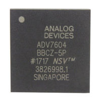
Analog Devices ADV7604 Hardware Manual (409 pages)
Component/Graphics Digitizer with 4:1 Multiplexed HDMI Receiver
Brand:
Analog Devices
| Category:
Computer Hardware
| Size: 2 MB
Table of Contents
Table of Contents
2
Disclaimer
8
Number Notations
8
Introduction to Adv7604 Hardware Manual
8
Description of Adv7604 Hardware Manual
8
Adv7604 Documentation Set
8
Register Access Conventions
9
Acronyms and Abbreviations
9
Field Function Description
10
References
11
Figure 1: Field Description Format
11
Introduction
13
Analog Front End
13
Hdmi Receiver
13
Component Processor
14
Main Features of Adv7604
15
Analog Front End
15
HDMI Receiver
15
Video Output Formats
15
Component Video Processing
15
Additional Features
16
RGB Graphics Processing
16
Functional Block Diagram
17
Figure 2: Functional Block Diagram
17
Pin Descriptions
18
Figure 3: ADV7604 Pin Configuration
18
Table 1: Pin Function Descriptions
18
Power Modes
28
Power-Down Modes
28
Adv7604 Revision Identification
28
Global Control Registers
28
Figure 4: Using +5 V from HDMI Source to Provide Supplies in Power-Down Mode 0
30
Figure 5: Hardware Configuration Recommended When PWRDNB Pin Required to Enter Power-Down Mode 0
31
Power-Save Mode
32
Secondary Power-Down Controls
33
ADC Power-Down Control
35
Reset Control
36
Crystal Frequencies Operation
36
Tristate LLC Driver
37
Global Pin Control
37
Tristate Pixel Bus Drivers
37
Tristate Synchronization Output Drivers
38
Tristate Audio Output Drivers
38
Drive Strength Selection (Data)
39
Drive Strength Selection (Clock)
40
Drive Strength Selection (Synchronization)
40
Synchronization Output Selection
41
Synchronization Output Signals Polarity
42
Figure 6: Synchronization Path
43
Digital Synthesizer Controls
44
Clock Generation for Analog CP Control
44
Phase Control
45
Dll on Llc Clock Path
45
Cp and Hdmi Simultaneous Mode
46
Pin Checker
47
Table 2: Pin Checker Values Corresponding to Output Pins
47
Table 3: Primary Mode and Video Standard Selection
49
Primary Mode and Video Standard
49
Primary Mode and Video Standard Controls
49
Table 4: V_FREQ[2:0] Description
53
Selecting Primary Mode and Video Standard for Hdmi Modes
54
Hdmi Decimation Modes
54
Primary Mode and Video Standard Configuration for Hdmi Free Run
55
Recommended Settings for Hdmi Inputs
55
Table 5: Recommended Settings for HDMI Inputs
55
Pixel Port Configuration
57
Llc Control
57
Cp Pixel Port Output Modes
57
Figure 7: Spreadsheet Screen Shot
57
Table 6: Sub Functions of OP_FORMAT_SEL[7:0]
58
Bus Rotation and Reordering Controls
59
Table 7: OP_FORMAT_SEL[7:0] Modes
59
Pixel Data and Synchronization Signals Control
60
Rounding and Truncating Data
61
Ddr Output Interface and Av Code Repetition
63
Analog Front End
64
Adc Sampling Clock Adjustment
64
Adcs and Voltage Clamps
64
ADC Power Control
64
ADC Input Range Control
64
Clamping
65
Figure 8: Video Signal Path to Adcs
65
Analog Input Muxing
66
Analog Input Routing Recommendation
66
Figure 9: Video Input Signal Level Prior to 24 Ohm to 51 Ohm Resistor Divider
66
Figure 10: Video Input Signal Level after Voltage Clamps
66
Auto Configuration
67
Recommended Analog Input Configurations
67
Table 8: ADC Input Muxing
67
Figure 11: Typical Configurations Using AIN_SEL[2:0]
68
Manual Input Muxing
68
Table 9: Manual Input Muxing
69
Sync 1, Sync 2, Sync 3 and Sync 4 Input Control
70
Figure 12: ADV7604 AFE Functional Diagram
70
Automatic Synchronization Configuration
71
Manual Synchronization Configuration
71
Manual Synchronization Application
72
Figure 13: Typical Example of Manual Synchronization Muxing
72
Table 10: Manual Synchronization Muxing Steps
72
Synchronization Strippers
73
Synchronization Filter Stage
73
Figure 14: Synchronization Stripper Circuit
73
Sync Stripper Slice Level
74
Tri 1-8 Input Control
74
Description
74
Table 12: D-Terminal Connector Characteristics (Bilevel)
75
Table 14: SCART Pin 8
75
Table 13: SCART Pin 16
75
SCART Connector
75
Table 11: D-Terminal Connector Characteristics (Trilevel)
75
TRI 1-8 Input Resistor Selection
75
D-Terminal Connector
75
Figure 15: D-Terminal Resistor Dividers
76
Figure 16: SCART Connector Resistor Dividers
76
Trilevel Slicers
77
Trilevel Slicer Operation
78
Figure 17: Trilevel Slicer
78
Bilevel/Trilevel Selection
79
Trilevel Slicer Readbacks
81
Slice Level Programming
83
Trilevel Interrupts
87
Table 15: Anti Alias Filter Frequency Characteristics
88
Anti Alias Filter Frequency Characteristics
88
Anti Alias Filter Control
88
Description
88
Anti Alias Filters
88
Figure 18: Anti Aliasing Filters Responses
89
Hdmi Receiver
90
Cable Detect
90
Figure 19: Functional Block Diagram of HDMI Core
90
Edid/Repeater Controller
92
Enhanced-Extended Display Identification Data Configuration
93
E-EDID Support for Power-Down Mode 0
94
Figure 20: SPI PROM Data Image Structure
97
Internal Edid
99
Edid Ram
99
Figure 21: Internal EDID RAM Map
99
Figure 22: Mapping between Internal EDID RAM and EDID Map
100
Structure of Internal E-EDID for Port a
101
Figure 23: Port a E-EDID Structure and Mapping
101
Figure 24: Port B E-EDID Structure and Mapping for SPA Located in EDID Block 1
102
Structure of Internal E-EDID of Ports B, C, and D
102
Figure 26: Port B E-EDID Structure and Mapping for SPA Located in EDID Block 3
103
Figure 25: Port B E-EDID Structure and Mapping for SPA Located in EDID Block 2
103
External E-Edid
106
Transition Minimized Differential Signaling Equalization
106
Figure 27: Low Frequency Gain Response
108
Figure 28: High Frequency Gain Response
108
Figure 29: Overall Gain of Equalizer Process
109
Port Selection
110
Tmds Clock Activity Detection
110
Clock and Data Termination Control
111
Tmds Measurement
112
TMDS Measurement after TMDS PLL
112
TMDS Measurement Prior to TMDS PLL
114
Figure 30: Monitoring TMDS Clock Frequency
114
Deep Color Mode Support
115
Video Fifo
116
Figure 31: HDMI Video FIFO
117
Pixel Repetition
120
Hdcp Support
121
HDCP Decryption Engine
121
Internal HDCP Key OTP ROM
122
HDCP Keys Access Flags
122
Figure 32: HDCP ROM Access after Power up
123
Figure 33: HDCP ROM Access after KSV Update from the Transmitter
123
Hdmi Synchronization Parameters
124
Horizontal Filters and Measurements
125
Horizontal Filter Locking Mechanism
125
Horizontal Filter Measurements
125
Figure 34: Horizontal Timing Parameters
127
Vertical Filters and Measurements
128
Figure 35: Vertical Parameters for Field 0
129
Figure 36: Vertical Parameters for Field 1
130
Figure 37: Audio Processor Block Diagram
131
Audio Control and Configuration
131
Audio DPLL
132
Audio FIFO
133
Table 16: Selectable Coast Conditions
133
Figure 38: Audio FIFO
134
Audio Packet Type Flags
135
Audio Output Controls
137
Figure 39: Monitoring Audio Packet Type Processed by ADV7604
137
MCLKOUT Setting
138
Audio Channel Mode
139
L-PCM and IEC 61937 Compressed Audio Interfaces
139
Figure 40: Timing Audio Data Output Via I
140
Figure 41: Timing Audio Data Output Via I
140
Figure 42: Timing Audio Data Output Via I
140
Table 17: I S/SPDIF Interface Description
140
Table 18: DSD Interface Description
141
Figure 45: AES3 Stream Timing Diagram
141
Figure 44: AES3 Sub-Frame Timing Diagram
141
Figure 43: IEC 60958 Sub-Frame Timing Diagram
141
DSD Interface
141
Figure 46: DSD Timing Diagram
142
HBR Interface
143
Table 19: HBR Interface Description
143
Audio Muting
144
Audio Mute Configuration
145
Table 20: Selectable Mute Conditions
147
Audio Stream with Incorrect Parity Error
150
Audio Clock Regeneration Parameters
150
ACR Parameters Readbacks
150
Monitoring ACR Parameters
151
Channel Status
152
Validity Status Flag
152
Figure 47: Reading Valid Channel Status Flags
153
General Control and Mode Information
154
Sampling and Frequency Accuracy
155
Source Number and Channel Number
155
Category Code
155
Word Length
156
Channel Status Copyright Value Assertion
157
Monitoring Change of Audio Sampling Frequency
157
Packets and Infoframes Registers
158
Infoframes Registers
158
Table 21: AVI Infoframe Registers
160
Table 22: Audio Infoframe Registers
162
Table 23: SPD Infoframe Registers
163
Table 24: MPEG Infoframe Registers
165
Table 25: VS Infoframe Registers
166
Packet Registers
167
Table 26: ACP Packet Registers
167
Table 27: ISRC1 Packet Registers
168
Table 28: ISRC2 Packet Registers
169
Table 29: Gamut Metadata Packet Registers
170
Customizing Packet/Infoframe Storage Registers
172
Repeater Routines Performed by the Edid/Repeater Controller
174
Repeater Support
174
Repeater Actions Required by External Controller
175
HDCP Registers Available in Repeater Map
177
Table 30: KSV List Registers Location
178
Table 31: Registers Location for SHA-1 Hash Value V
180
Interface to Dpp Section
181
Figure 48: YC 4:2:2 Video Data Encapsulated in HDMI Stream
181
Figure 49: Video Stream Output by HDMI Core for YC
181
Figure 50: Video Data Output by DPP in 4:2:2 Pass through Mode
183
Color Space Information Sent to the Dpp and Cp Sections
183
Status Registers
184
Table 32: HDMI Flags in IO Map Register 0X60
184
Table 33: HDMI Flags in IO Map Register 0X65
184
Table 34: HDMI Flags in IO Map Register 0X6A
185
Table 35: HDMI Flags in IO Map Register 0X6F
185
Table 36: HDMI Flags in IO Map Register 0X74
185
Table 37: HDMI Flags in IO Map Register 0X79
186
Table 40: HDMI Flags in HDMI Map
187
Table 38: HDMI Flags in IO Map Register 0X7E
187
Table 39: HDMI Flags in IO Map Register 0X83
187
Hdmi Section Reset Strategy
188
Decimation and Color Space Conversion
189
Data Preprocessor
189
Dpp Enable Control
189
Figure 51: DPP Block Diagram
189
Decimation Filters
190
DPP Automatic Selection
191
Decimation Filter Selection for Stage 1
191
Table 41: DPP Filter Auto Selection
191
Figure 52: Manual and Default DCM Filter Response Selection
192
Decimation Filter Selection for Stage 2
193
Figure 53: DPP Predetermined Filter Responses Available in Manual Selection Mode
194
Table 42: Coefficients of 19-Tap Decimation Filter on Channel a
195
Table 43: Coefficients of 19-Tap Decimation Filters on Channels B and C
196
Chroma 4X Decimation Filter Selection in Stage 2
197
Figure 54: Chroma 4X Filter Responses in Manual Selection Mode
198
DPP Decimation Only Selection
198
Figure 55: Channel B/C Decimation by 2 for Fs = 13.5 Mhz
199
Figure 56: Default Channel B/C Decimation by 2 with DPP_CHROMA_LOW_EN = 1 for Fs = 13.5 Mhz
199
Figure 57: Default Channel A/D Decimation by 2, Channel B/C Decimation by 2 and 4 for Fs = 27 Mhz
200
Figure 58: Default Channel A/D Decimation by 2, Channel B/C Decimation by 2 and 4 with DPP_CHROMA_LOW_EN = 1 for Fs = 27 Mhz
200
Figure 59: Default Channel A/D Decimation by 4, Channel B/C Decimation by 4 and 8 for Fs = 54 Mhz
201
Figure 60: Default Channel A/D Decimation by 4, Channel B/C Decimation by 4 and 8 with DPP_CHROMA_LOW_EN = 1 for Fs = 54 Mhz
201
Figure 62: Configuring DPP/CP CSC Blocks
202
Figure 61: DPP/CP CSC Block Diagram
202
Color Space Conversion Matrix
202
CP CSC or DPP CSC Selection
203
Selecting Auto or Manual CSC Conversion Mode
204
Auto Color Space Conversion Matrix
205
Table 44: Automatic Input Color Space Selection
205
Table 45: Automatic CSC Selection
206
Table 46: CSC Configuration for All CSC Modes Reported by CSC_COEFF_SEL_RB
207
Figure 64: ADV7604 HDMI Auto CSC Flowchart (Case RGB)
208
HDMI Auto CSC Operation
208
Figure 63: ADV7604 HDMI Auto CSC Flowchart
208
Figure 65: ADV7604 HDMI Auto CSC Flowchart (Case Ycbcr-1)
209
Figure 66: ADV7604 HDMI Auto CSC Flowchart (Case Ycbcr-2)
209
Figure 67: ADV7604 Manual RGB Range Control Flowchart for Auto CSC (Case RGB)
210
Manual Color Space Conversion Matrix
211
Figure 68: Single CSC Channel
211
Table 47: CSC Coefficients
212
CSC in Pass-Through Mode
216
Color Controls
217
Enhanced Standard Definition Processor
219
Background
219
Modes of Operation
219
Datapath Summary
219
Clamp and Gain
220
Figure 69: ESDP Block Diagram
220
Vsync/Field Separation
221
Hsync Separation
221
Input Signal Detection
221
Output Timing Signals
222
Table 48: Synchronization Timing Adjustment Controls
222
Basic Control - Enabling/Disabling ESDP Mode
223
Nonstandard Samples Per Line
224
Esdp Free Run Mode
225
Table 49: ESDP Setup Examples
225
Figure 70: Component Processor Block Diagram
226
Introduction to Component Processor
226
Component Processor
226
Clamp Operation
227
Figure 71: Position of Voltage Clamp Window
227
Cp Gain Operation
230
Features of Manual Gain Control
230
Features of Automatic Gain Control
230
Manual Gain and Automatic Gain Control Selection
231
Table 50. Input Ranges for HDMI Modes
231
Figure 72: CP Automatic Gain Controls
232
Manual Gain Control
233
Manual Gain Filter Mode
235
Automatic Gain Control
235
CP Peak Active Video Readback
239
Table 51: OP_656_RANGE Description for HDMI Receiver Input Mode
239
Table 52: OP_656_RANGE Description for Analog Front End Input Mode
239
Cp Offset Block
241
Figure 73: Channel A, B, and C Automatic Value Selection
241
Av Code Block
242
Figure 74 AV Code Output Options (CP)
244
Cp Data Path for Analog and Hdmi Modes
245
Pregain Block
245
Table 53: Settings Required to Support Extended Range Video Input
245
Figure 75: CP DATA Path Channel a (Y) for Analog Mode
246
Figure 76: CP Data Path Channel B/C (UV) for Analog Mode
247
Figure 77: CP Data Path Channel A/B/C (RGB) for Analog Mode
248
Figure 78: CP Data Path Channel a (Y) for HDMI Mode
249
Figure 79: CP Data Path Channel B/C for HDMI Mode
250
Synchronization Processed by Cp Section
251
Sync Extracted by ESDP Block
251
Figure 80: Syncs Extracted by ESDP Section
251
Sync Extracted by Sync Slicer Section
252
Figure 81: Sliced Signal Path
252
External Sync and Sync from HDMI Section
253
Figure 82: External/Hdmi Syncs Routing to CP Section
253
Final Sync Muxing Stage
256
Synchronization Processing Channel Mux
257
Figure 83: Final Sync Muxing Stage
257
Synchronization Source Polarity Detector
259
Figure 84: SSPD Auto Detection Flowchart
260
Figure 85: SSPD Vsync and Hsync Monitoring Operation
266
Standard Detection and Identification
267
Detailed Mechanism of STDI Block Horizontal/Vertical Lock Mechanism
270
Figure 87: STDI Hsync Monitoring Operation
271
Figure 86: STDI Horizontal Locking Operation
271
Figure 88: STDI Vertical Locking Operation
272
Figure 89: STDI Vsync Monitoring Operation
272
Figure 90: STDI Usage Flowchart
274
Table 54: STDI Readback Values for SD, PR, and HD
275
Table 55: STDI Results for Graphics Standards
275
Figure 91: STDI Values for GR Mode (Plot)
276
Cp Output Synchronization Signal Positioning
277
Figure 92: ADV7604 Synchronization Signal Processing Flow Diagram
277
Figure 93: Synchronization Repositioning and Displayed Area
278
Table 56: CP Synchronization Signal Output Pins
278
CP Primary Synchronization Signals
279
Hsync Timing Controls
279
Table 57: HS Default Timing
279
Table 60: HS Default Timing (Continued 3)
280
Table 59: HS Default Timing (Continued 2)
280
Table 58: HS Default Timing (Continued 1)
280
Figure 94: HS Timing
281
Vsync Timing Controls
283
Table 61: VS Default Timing
283
Timing Controls
284
FIELD Timing Controls
285
Table 62: FIELD Default Timing
285
Figure 95: 525I VS Timing
287
Figure 96: 625I VS Timing
288
Figure 97: 525P VS Timing
289
Figure 98: 625P VS Timing
289
Figure 99: 720P VS Timing
290
Figure 100: 1080I VS Timing
291
Figure 101: 1080P VS Timing
292
Secondary Synchronization Signals
293
Ancillary Synchronization Signal Outputs
293
Figure 102: Ancillary Synchronization Information Output on VS/FIELD Pin
294
Figure 103: Ancillary Synchronization Information Output on SYNC_OUT/INT2 Pin
296
Cp Horizontal Lock Status
296
Figure 104: Synchronization Lock Robustness Measurement
297
Noise and Calibration
298
Measurement Window
298
Noise Measurement
298
Calibration Measurement
299
Cp Hdmi Controls
299
Free Run Mode Thresholds
300
Free Run Mode
300
Free Run Feature in HDMI Mode
303
Figure 105: Free Run Field Length Selection for Channel 1 and Channel 2
303
Free Run Default Color Output
304
Table 63: Default Color Output Values (CP)
304
Cp Status
307
Auto Graphics Mode
308
Primary Auto Graphics Controls
308
Secondary Auto Graphics Control
309
Auxiliary Auto Graphics Controls
311
Setting Examples for 1280X720P
312
External Clock and Clamp Mode Operation
312
Introduction to External Clock and Clamp Mode
312
Figure 106: System Delay for External Clock and Clamp Mode
313
Clamp Control
314
Figure 107: External Clock and Clamp Mode Block Diagram
314
Configuring External Clock and Clamp Mode
315
Table 64: ADV7604 External Clock and Clamp Modes
315
Figure 108: Regenerated Clamp Pulse Position Control
318
System Delay in ADV7604
320
Figure 109: System Delay in ADV7604
320
Table 65: Delay Clock Cycles for Various Operation Modes
321
Vbi Data Processor
322
Vdp Configuration
322
VDP Default Configuration
323
Table 66: VBI Data Standards
323
Table 67: Default Standards on Lines for Supported Interlaced and Progressive Standards
323
Table 68: Details of Manual Line Programming Registers
324
VDP Manual Configuration
324
Table 69: Details of Full Field/Frame Programming Registers
326
Full Field/Frame Detection
326
Teletext System Identification
326
Vdp Configuration
327
Hamming Code Error
328
Table 70: Error Bits in Dehammed Output Byte
328
Table 71: WST Packet Description
328
Adaptive Slice Level Generators
331
Vdp Ancillary Data Output
332
Nibble Output Mode
333
Table 73: Ancillary Data in Byte Output Format
334
Table 72: Ancillary Data in Nibble Output Format
334
Structure of Vbi Words in Ancillary Data Stream
335
Table 74: Structure of VBI Data Words in Ancillary Stream
335
Framing Code
336
Table 75: Framing Code Sequence for Different VBI Standards
336
Data Bytes
337
Table 76: Total User Data Words for Different VBI Standards
337
Register Readback Protocol
338
Readback Registers
338
User Interface for Readback Registers
338
Content Based Data Update
339
Interrupt Based Reading of I C Registers
340
Interrupt Mask Register Details
341
Interrupt Status Register Details
342
Interrupt Status Clear Register Details
343
C Readback Egisters
343
Teletext
343
CGMS and WSS
344
Figure 110: WSS (625I) Waveform
344
Ccap
345
Figure 111: CGMS (525I) Waveform
345
Vitc
346
Figure 112: CCAP Waveform and Decoded Data Correlation
346
Table 77: VITC Readback Registers
347
Figure 113: VITC Waveform and Decoded Data Correlation
347
VPS, PDC, UTC, Gemstar, and CGMS Type B
347
Table 78: VDP_GS_VPS_PDC_UTC_CGMSTB_DATA Readback Registers
348
Table 79: VDP_CGMS_TYPEB_DATA Readback Registers
350
Customer Electronic Control
351
Figure 114: CEC Block Diagram
351
Main Controls
352
Cec Transmit Module
352
Table 80: CEC Outgoing Message Buffer Registers
352
Figure 115: State Machine of CEC Transmitter
355
Cec Receiver Module
356
Table 81: CEC Incoming Message Buffer Registers
356
Clock
358
Odule
358
Figure 116: State Machine of CEC Receiver
358
Initializing CEC Module
359
Typical Operation Flow
359
Antiglitch Filter Module
359
Figure 118: Using CEC Module as Initiator
360
Using CEC Module as Initiator
360
Figure 117: CEC Module Initialization
360
Using CEC Module as Follower
361
Figure 119: Using CEC Module as Follower
361
Av.link Bus Interface
362
Figure 120: Av.link Block Diagram
362
Av.link Transmit Module
363
Table 82: Av.link Outgoing Message Buffer Registers
363
Main Controls
363
Figure 121: Av.link Command Block
364
Av.link Receive Module
366
Figure 122: Transmitter Core State Machine
366
Table 83: Av.link Incoming Message Buffer Registers
367
Figure 123: Av.link Receiver State Machine
369
Format Description of Transmitted Frames
370
Table 84: Start Sequence Table
370
Odule
370
Av.link Antiglitch Filter
370
Clock
370
Mode 1
371
Mode 2
371
Mode 3
371
Figure 124: Mode 1 Frame Format
371
Figure 125: Mode 2 Frame Format
371
Figure 126: Mode 3 Frame Format
371
Table 85: Value Taken by each Data Unit in Mode 1 Frame
371
Table 86: Value Taken by each Data Unit in Mode 2 Frame
371
Mode Detection
372
Table 87: Value Taken by each Data Unit in Mode 3 Frame
372
Esc/Dir Bit Validation
373
Figure 127: Pseudo C Code for Mode Detection
373
Figure 128: Pseudo C Code for ESC/DIR Bit Validation
373
Interrupt Request Output Operation
374
Interrupts
374
Interrupt Manual Assertion
375
Multiple Interrupt Events
375
Interrupt Drive Level
375
HDMI Interrupts Validity Checking Process
376
Table 88: Interrupt Functions Available in ADV7604
376
Table 89: HDMI Interrupts in IO Map Categorized into Three Groups
377
Table 90: HDMI Interrupts Group 1
377
Table 91: HDMI Interrupts Group 2
377
Table 92: HDMI Interrupts Group 3
378
Storing Masked Interrupts
379
Processing AFE Interrupts
380
Figure 129: Processing Trilevel Interrupts
381
Hardware Design
382
Power Supply Sequence
382
Register Access
383
Figure 130: ADV7604 Register Map Access through Main I C Port
383
Port
383
Register Access and Serial Ports Description
383
Protocol for Main I C Port
384
Table 93: Register Maps and I
384
DDC Ports
385
I 2 C Protocols for Access to the Internal EDID
385
Figure 131: Bus Data Transfer
385
Figure 132: Read and Write Sequence
385
I 2 C Protocols for Access to HDCP Registers
386
DDC Port B
386
Figure 133: Internal E-EDID and HDCP Registers Access from Port a
386
DDC Port a
386
DDC Port C
387
DDC Port D
387
Figure 134: Internal E-EDID and HDCP Registers Access from Port B
387
Figure 135: Internal E-EDID and HDCP Registers Access from Port C
387
Figure 136: Internal E-EDID and HDCP Registers Access from Port D
388
Power Supply Bypassing
389
Pcb Layout Recommendations
389
Analogue Interface Inputs
389
Hdmi Inputs
390
Digital Outputs (Data and Clocks)
390
Figure 137: Recommended Power Supply Decoupling
390
Digital Inputs
391
Xtal and Load Cap Value Selection
391
Figure 138: Crystal Circuit
391
Table 94: Recommended Configuration for Unused Pins
393
Recommended Configuration for Unused Pins
400
Package Outline Drawing
400
Ordering Guide
400
Figure 139: BGA Package
400
Adv7604 List of Figures
401
List of Figures
401
List of Tables
403
List of Equations
405
Document Revision History
406
Advertisement
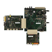
Analog Devices ADV7604 User Manual (27 pages)
Brand:
Analog Devices
| Category:
Motherboard
| Size: 1 MB
Table of Contents
Table of Contents
2
1 Introduction
3
2 Evaluation Kit
3
3 Initial Configuration
4
Hardware
4
Software
5
ATV Benchtop Installation
5
Getting Started with ADV Register Control Software
5
4 Using the Evaluation Platform
7
ADV7604 Evaluation Board Hardware
7
Connecting Input Video
8
EDID Configuration
8
Powerdown Mode EDID
9
Video Output Module
10
Using Configuration Scripts
10
Using Software Driver
11
Configuring the Motherboard
11
5 Updating Files
12
Updating Scripts
12
Updating Defaults
12
6 Schematics
13
7 Layout
22
Advertisement
Related Products
Analog Devices ADV7281-M
Analog Devices ADV3221-EVALZ
Analog Devices ADV3222-EVALZ
Analog Devices ADV3222
Analog Devices MICROCONVERTER ADUC814-28TSSOP
Analog Devices ADUCM310BBCZ-RL
Analog Devices AD9166-FMC-EBZ
Analog Devices AD9117
Analog Devices AD9520-3
Analog Devices AD7766-2
Analog Devices Categories
Motherboard
Computer Hardware
Controller
Media Converter
Extender
More Analog Devices Manuals
Login
Sign In
OR
Sign in with Facebook
Sign in with Google
Upload manual
Upload from disk
Upload from URL