Table of Contents
Advertisement
Advertisement
Table of Contents

Related Manuals for Siemens ERTEC 200P-2


Summary of Contents for Siemens ERTEC 200P-2
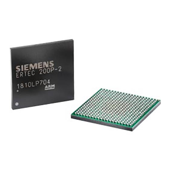
- Page 1 ERTEC 200P-2 Enhanced Real-Time Ethernet Controller Manual...
- Page 2 DOCUMENTS, NOR DOES SIEMENS ADOPT THESE WEB SITES AND ELECTRONIC DOCUMENTS AND THEIR CONTENTS AS THEIR OWN. YOU THEREFORE USE THESE LINKS AT YOUR OWN RISK. SINCE SIEMENS IS NOT RESPONSIBLE FOR LINKED CONTENTS AND INFORMATION ON THE WEB SITES AND ELECTRONIC DOCUMENTS OF THIRD PARTIES, THIS INFORMATION IS NOT CHECKED BY SIEMENS.
- Page 3 Section 5 Package o Section 6 Quality o Section 7 Miscellaneous Scope of the Manual This manual applies to the following product: ERTEC 200P-2 Copyright © Siemens AG 2016. All rights reserved ERTEC 200P-2 Manual Technical data subject to change Version 1.0...
- Page 4 Johnson City, TN 37602- 4991 Technical Contacts for China PIC China: Mr. Xu Bin 7,Wangjing Zhonghuan Nanku E-mail: Profinet.cn@siemens.com 100102 BEIJING Copyright © Siemens AG 2016. All rights reserved ERTEC 200P-2 Manual Technical data subject to change Version 1.0...
- Page 5 In order to protect plants, systems, machines and networks against cyber threats, it is necessary to implement – and continuously maintain – a holistic, state-of-the-art industrial security concept. Siemens’ products and solutions only form one element of such a con- cept.
-
Page 6: Table Of Contents
APB Subsystem (Peripheral Bus) ..................47 2.3.2.4.1 APB Decoder .........................51 2.3.2.5 Address Range and Acknowledgement Delay Monitoring .............51 2.3.2.5.1 Monitoring at the AHB Side ....................51 Copyright © Siemens AG 2016. All rights reserved ERTEC 200P-2 Manual Technical data subject to change Version 1.0... - Page 7 Function Description (XHIF) ....................183 2.3.6.2.1 AHB Master Interface ....................186 2.3.6.2.2 APB Slave Interface .....................186 2.3.6.2.3 XHIF Configuration .......................186 2.3.6.2.4 Application Information ....................187 Copyright © Siemens AG 2016. All rights reserved ERTEC 200P-2 Manual Technical data subject to change Version 1.0...
- Page 8 Register Description ....................286 2.3.10.4 F-Counter ........................302 2.3.10.4.1 Function Description ....................303 2.3.10.4.2 Application Information ....................303 2.3.10.4.3 Address Mapping .......................303 2.3.10.4.4 Register Description ....................304 Copyright © Siemens AG 2016. All rights reserved ERTEC 200P-2 Manual Technical data subject to change Version 1.0...
- Page 9 2.4.4 Host IF Memory Mapping .......................418 2.4.5 GDMA Memory Mapping ......................421 Detailed Address Mapping ......................422 Register Description ........................425 IO INTERFACE ......................426 Copyright © Siemens AG 2016. All rights reserved ERTEC 200P-2 Manual Technical data subject to change Version 1.0...
- Page 10 Circuit with Ext. Crystal ......................476 4.2.2 Circuit with External Crystal Oscilllator ...................478 PLL Wiring (Power Supply) ......................479 Test Signal Configuration ......................480 JTAG Wiring ..........................480 Copyright © Siemens AG 2016. All rights reserved ERTEC 200P-2 Manual Technical data subject to change Version 1.0...
- Page 11 Tray ............................498 5.6.2 Tape&Reel ..........................498 QUALITY ........................499 Hard-Error FIT rates ........................499 Soft-Error FIT rates........................499 MISCELLANEOUS ....................500 Abbreviations ..........................500 Literature list ..........................501 Copyright © Siemens AG 2016. All rights reserved ERTEC 200P-2 Manual Technical data subject to change Version 1.0...
- Page 12 Figure 41: SPI flash: serial output timing Figure 42: SPI flash: serial input timing Figure 43: Block diagram of a GPIO module Figure 44: GPIO, IO Circuit Copyright © Siemens AG 2016. All rights reserved ERTEC 200P-2 Manual Technical data subject to change Version 1.0...
- Page 13 Figure 56: FX circuit unused pins Figure 57: SD level translation circuit Figure 58: Recommendation for handling special function signals Figure 59: 400-ball SIP-FPBGA Copyright © Siemens AG 2016. All rights reserved ERTEC 200P-2 Manual Technical data subject to change Version 1.0...
- Page 14 Table 23: Configuration adjustment Table 24: IO – pin count overview Table 25: Signal Description and Pinning ERTEC 200P Table 26: Constraining PNPLL Interface Copyright © Siemens AG 2016. All rights reserved ERTEC 200P-2 Manual Technical data subject to change Version 1.0...
-
Page 15: Introduction
With IRT, cyclic communication operates in reserved time phases. You can choose between address-based forwarding and topological forwarding (planned communica- tion). The cut through time is ca. 2.1 µs (incl. PHY). Copyright © Siemens AG 2016. All rights reserved ERTEC 200P-2 Manual Technical data subject to change... -
Page 16: Mechanisms For Profinet Io (Irt High Performance Communication) Rtc3
Note: Branches and merges are possible; however, the configuration required for deterministic behav- ior and the possible times are more difficult to define. Copyright © Siemens AG 2016. All rights reserved ERTEC 200P-2 Manual Technical data subject to change... -
Page 17: Ertec 200P Data
1x I C (in PN-IP for fiber-optic transceiver) 4x UART including one UART as default without alternate function 2x SPI1 (master / slave,) Copyright © Siemens AG 2016. All rights reserved ERTEC 200P-2 Manual Technical data subject to change Version 1.0... -
Page 18: System Reliability
These standards are the device standards for use in industrial environments. For com- pliance with these device standards, however, the EMC of the individual integrated circuits used (in particular immunity to interference in operation) is key. Copyright © Siemens AG 2016. All rights reserved ERTEC 200P-2 Manual Technical data subject to change... -
Page 19: Ertec 200P Use Cases
PN-IP and by the host. The PN-IP transfers the data into the IO-RAM of the PER-IF. The host then transfers the data from there to its application. Copyright © Siemens AG 2016. All rights reserved ERTEC 200P-2 Manual Technical data subject to change Version 1.0... -
Page 20: Use Case 2 (Uc2): Operation Without External Host
The following profile is supported: - PN stack and application are combined as sources - Time-critical application code ( 256 kbytes) can be loaded into the integrated RAM Copyright © Siemens AG 2016. All rights reserved ERTEC 200P-2 Manual Technical data subject to change... -
Page 21: Application Notes
The user should pay attention to the following application notes: 1.4.1 EMC SDRAM Interface The EMC of the ERTEC 200P-2 has two possible settings for clocked signal output (address, data and control signals) to an external SDRAM. These can be configured over EXTENDED_CONFIG.SODM (see 2.3.5.8):... -
Page 22: Emc Burst Flash Interface
CLKOB and CLKOC do not. As multiplication (factor of 20) of the quartz clock (25 MHz) to 500 MHz is only possible at the CLKOB output (a Copyright © Siemens AG 2016. All rights reserved ERTEC 200P-2 Manual Technical data subject to change Version 1.0... -
Page 23: 16-Bit Data Access Over Xhif In Buffered Mode
XHIF. This write access always uses the data buffered in the XHIF and the data currently pending, and applies to the address currently pending at the XHIF and implemented at AHB. Copyright © Siemens AG 2016. All rights reserved ERTEC 200P-2 Manual Technical data subject to change... -
Page 24: Description Of Functions
The main requirements governing development of ERTEC 200 ERTEC 200P Step1 were: - USABILITY - PERFORMANCE ERTEC 200P Step1 -> ERTEC 200P-2 redesign implements the following key aspects: 1. System redundancy Rapid backup Primary switching (no waiting time to ensure data status consistency) 2. gPTP support 3. -
Page 25: Description Of Individual Ertec 200P Blocks
TCM is with a 'DMA-DTCM Access Controller'. I-TCM is only operated by ARM926EJ-S and cannot be accessed by the AHB. ARM926EJ-S is described in detailed under /7/. Copyright © Siemens AG 2016. All rights reserved ERTEC 200P-2 Manual Technical data subject to change... -
Page 26: Features
Memory Management Unit (MMU) Little endian support only Operating frequency: 125/250MHz ARM926 125MHz AMBA bus system Process: CB-90 2.3.1.2 Block diagram Figure 5: ARM926 subsystem Copyright © Siemens AG 2016. All rights reserved ERTEC 200P-2 Manual Technical data subject to change Version 1.0... -
Page 27: Arm926Ej-S Processor
SW (each cache line must be initialized in a loop). Until this point, the parity logic is disabled. Control is with the SCRB register Copyright © Siemens AG 2016. All rights reserved ERTEC 200P-2 Manual Technical data subject to change Version 1.0... -
Page 28: Arm926 Tightly Coupled Memories (Arm926_Tcm)
'EDC_Event' IRQ48 is triggered (see 2.3.2.14 ). '0h' must be written to the EDC event register to clear the error. 1 KByte is equal to 1024 bytes. Copyright © Siemens AG 2016. All rights reserved ERTEC 200P-2 Manual Technical data subject to change Version 1.0... -
Page 29: Memory Management Unit (Mmu)
A fast context switch enables virtual address remapping in a 0 – 32 MByte area TLB entries can be locked The MMU RAMs are not assigned parity. Copyright © Siemens AG 2016. All rights reserved ERTEC 200P-2 Manual Technical data subject to change... -
Page 30: Bus Interface Of The Arm926 Processor
The medium+ ETM9 cell has a larger FIFO (18 -> 45 bytes). ETM trace condition configuration is only possible from the external debugger and not over the AHB interface of the ETB11. Copyright © Siemens AG 2016. All rights reserved ERTEC 200P-2 Manual Technical data subject to change... -
Page 31: Debug Support
Before these debug signals can be used, they must be enabled in the GPIO31-0 block. If DBGREQ is not enabled in its alternate function, DBGREQ is internally not active and ARM926EJ-S is not in the debug state. Copyright © Siemens AG 2016. All rights reserved ERTEC 200P-2 Manual Technical data subject to change... -
Page 32: Boot Process For The Ertec 200P
The secondary boot loader sets the final TCM926 configuration required in TCM926_MAP (see 2.3.10.9.14). The code image can then be transferred by the boot medium to the I-TCM after the secondary boot loader. Copyright © Siemens AG 2016. All rights reserved ERTEC 200P-2 Manual Technical data subject to change... - Page 33 This also allows a wide range of different compilers, without having to consider special features such as INIT or ROM sections. Copyright © Siemens AG 2016. All rights reserved ERTEC 200P-2 Manual Technical data subject to change...
-
Page 34: Primary Boot Loader
Stack pointer from address: 0x0800_FA00 0x0c Opcode from Jump command after illegal opcode address is read illegal ad- Stack pointer from address: 0x0800_FB00 Copyright © Siemens AG 2016. All rights reserved ERTEC 200P-2 Manual Technical data subject to change Version 1.0... - Page 35 SPI master (RD Cmd: 0x03) XHIF (ext. host) The secondary boot loader is run straight from the NOR flash and not from the TCM. The default mode, Copyright © Siemens AG 2016. All rights reserved ERTEC 200P-2 Manual Technical data subject to change...
-
Page 36: Table 3: Boot Mode Adjustment
Compile mode bit),ASYNC_ ADDR_MODE = 1 5.8 ms (256 data bytes copied) 1.07 ms SPI master (RD Cmd: Each additional byte requires Copyright © Siemens AG 2016. All rights reserved ERTEC 200P-2 Manual Technical data subject to change Version 1.0... -
Page 37: Boot Mode 1
The complete interrupt vector table is available in the boot ROM to prevent system dead- lock. When an interrupt or an exception occurs, a restart is always carried out if the vector Copyright © Siemens AG 2016. All rights reserved ERTEC 200P-2 Manual Technical data subject to change Version 1.0... -
Page 38: Boot Modes 5 And 6 (Booting With Spi Master)
If an identifier is read for one of the two read commands (ID_OK = 0x5A), the position of the identifier in the SPI data stream indicates how many address bytes (1, 2, 3 or 4 bytes) Copyright © Siemens AG 2016. All rights reserved ERTEC 200P-2 Manual Technical data subject to change Version 1.0... - Page 39 Word 1 TCM+5 0x00 Data 5 TCM+6 0x01 Data 6 TCM+7 0x05 Data 7 TCM+8 0x00 Data 8 TCM+0x104 ….. ….. ….. Copyright © Siemens AG 2016. All rights reserved ERTEC 200P-2 Manual Technical data subject to change Version 1.0...
-
Page 40: Boot Mode 7 (Booting With External Host)
XHIF host sets identifier 0x6879_9786 at address D- TCM+0x40 (address 0x0803_0040 in block 3 of the D-TCM) (semaphore address). Note for module development Copyright © Siemens AG 2016. All rights reserved ERTEC 200P-2 Manual Technical data subject to change... - Page 41 IMPORTANT: The interrupt vector table (see 2.3.1.5.1) is to be stored at the addresses before the semaphore (i.e. from addresses 0x0803_0000) Copyright © Siemens AG 2016. All rights reserved ERTEC 200P-2 Manual Technical data subject to change Version 1.0...
- Page 42 Value == expectedValue external host can configure additional pages XHIF Ready Flow chart for the external host for establishing XHIF interface enable Copyright © Siemens AG 2016. All rights reserved ERTEC 200P-2 Manual Technical data subject to change Version 1.0...
-
Page 43: Secondary Boot Loader
2.3.2.1 Characteristics of the Bus System in ERTEC 200P The table below sets out the characteristics of the internal bus system: Copyright © Siemens AG 2016. All rights reserved ERTEC 200P-2 Manual Technical data subject to change... -
Page 44: Endianness
AMBA AHB interface are implemented more efficiently by using an AMBA AXI protocol interface. More detailed documentation is available at: /11/ AHB_Lite_Protocol. Copyright © Siemens AG 2016. All rights reserved ERTEC 200P-2 Manual Technical data subject to change... -
Page 45: Ahb Arbiters
No fixed priority is assigned to the PN-IP-M2 master as the connection to the PER-PN-S10 is point-to-point. This prevents a conflict from ever occurring at PER-PN-S10. Copyright © Siemens AG 2016. All rights reserved ERTEC 200P-2 Manual Technical data subject to change... -
Page 46: Ahb Burst Breaker
IDLE cycles in between, which are necessary for re-arbitration of AHB masters. The Burst Breaker counts the address phases of following ARM926-D/ARM926-I AHB transfers: SINGLE INCR unspecified length Copyright © Siemens AG 2016. All rights reserved ERTEC 200P-2 Manual Technical data subject to change Version 1.0... -
Page 47: Apb Subsystem (Peripheral Bus)
ERTEC 200P has a wider functionality than the ARM-APB bus (see document /11/, 5.5). Unlike the standard APB bus, it offers the option of variable timing (wait states) and byte Copyright © Siemens AG 2016. All rights reserved ERTEC 200P-2 Manual Technical data subject to change Version 1.0... - Page 48 The AHB/APB bridge is implemented between the two buses. The AHB/APB bridge has a single-stage write buffer. The function of the AHB bridge is detailed in document /40/ AHB_APB_BRIDGE_V1.0- pdf. Copyright © Siemens AG 2016. All rights reserved ERTEC 200P-2 Manual Technical data subject to change Version 1.0...
-
Page 49: Figure 7: Ahb/Apb Bridge, Block Diagram
PBExx which exist in parallel to PADDR, i.e. PADDR and PBE timing are identical (see Figure 8: APB bridge, timing with sideband Copyright © Siemens AG 2016. All rights reserved ERTEC 200P-2 Manual Technical data subject to change... -
Page 50: Figure 8: Apb Bridge, Timing
AHB_APB_Bridge therefore synchronous reset has to be applied to meet recov- ery/removal time requirements. Bridge timing with the additional signals PBE and PRDY: Figure 8: APB bridge, timing Copyright © Siemens AG 2016. All rights reserved ERTEC 200P-2 Manual Technical data subject to change Version 1.0... -
Page 51: Apb Decoder
ARM926 core. Address gaps in the APB address range are not visible at the AHB side; the monitoring mechanisms in 2.3.2.5.2 apply. Copyright © Siemens AG 2016. All rights reserved ERTEC 200P-2 Manual Technical data subject to change Version 1.0... -
Page 52: Monitoring At The Apb Side
An entry in the module register Access_Error is saved when ERR_LOCK = '0' in the fol- lowing cases: Write access to read-only registers Write and read access to address gaps in register and RAM address ranges Copyright © Siemens AG 2016. All rights reserved ERTEC 200P-2 Manual Technical data subject to change Version 1.0... -
Page 53: Table 8: Access Error Register (From Scrb)
MODUL_ACCESS_ERR register to identify the module affected. The SW must then read the detailed data for the erroneous access from the access error register in the relevant Copyright © Siemens AG 2016. All rights reserved ERTEC 200P-2 Manual Technical data subject to change... -
Page 54: Overview
Copyright © Siemens AG 2016. All rights reserved ERTEC 200P-2 Manual Technical data subject to change Version 1.0... -
Page 55: Interrupt Acquisition
In edge-triggered mode, each level on the input for synchronous signals must be stable for at least one clock, for asynchronous signals for at least two clocks. Copyright © Siemens AG 2016. All rights reserved ERTEC 200P-2 Manual Technical data subject to change... - Page 56 – and only in this regard – the software interrupt is always treated as level-triggered. Copyright © Siemens AG 2016. All rights reserved ERTEC 200P-2 Manual Technical data subject to change...
-
Page 57: Interrupt Masking / Priorisation
LOCKREG register. If the interrupt request has already been pending longer without it being acknowledged and the software now writes this LOCKREG with the same Copyright © Siemens AG 2016. All rights reserved ERTEC 200P-2 Manual Technical data subject to change... -
Page 58: Interrupt Post-Processing
The Interrupt Controller Unit does not require any further information from the CPU to identify the interrupt whose bit must be cleared in the ISREG (non-specific EOI com- mand). Copyright © Siemens AG 2016. All rights reserved ERTEC 200P-2 Manual Technical data subject to change... -
Page 59: Special Functions
MASK_ALL_INPUT_EN software register. The input is synchronized by the ICU with a double flop. In ERTEC 200P this input is tied inactive. 2.3.2.13 Miscellaneous 2.3.2.13.1 Synchronizing the inputs Copyright © Siemens AG 2016. All rights reserved ERTEC 200P-2 Manual Technical data subject to change Version 1.0... -
Page 60: Bus Interface
This is mandatory since the CPU issues an end-of-interrupt command after the execution of the interrupt service routine, by carrying out a write access to Copyright © Siemens AG 2016. All rights reserved ERTEC 200P-2 Manual Technical data subject to change... -
Page 61: Operating Rules
(described is a writing on the first and immediate reading of the second register): IRCLVEC -> ACK IRCLVEC -> IRREG1-5 IRCLVEC -> SWIRREG1-5 LOCKREG -> ACK MASK -> ACK ACK->IRREG1-5 Copyright © Siemens AG 2016. All rights reserved ERTEC 200P-2 Manual Technical data subject to change Version 1.0... -
Page 62: Startup/Shutdown
INTA input in the INTA sub-block used as INTB since otherwise an INTA as well as an INTB is signaled to the CPU upon the occurrence of the interrupt. Copyright © Siemens AG 2016. All rights reserved ERTEC 200P-2 Manual Technical data subject to change Version 1.0... -
Page 63: Interrupt Sources For Arm-Irq
Receive FIFO half-full or full TR (group inter- Transmit FIFO half-empty or rupt) empty Receive Timeout UART4_UARTEI INT_UART4_ER Error interrupt (Error interrupt) Copyright © Siemens AG 2016. All rights reserved ERTEC 200P-2 Manual Technical data subject to change Version 1.0... - Page 64 INT_TIMER5 TIM_OUT5 Timer expired (value 0 reached) WD_INT_ARM9 Watchdog ARM926 Watchdog Inter- ARM926 rupt SPI1_TFE SPI1_TFE Transmit FIFO empty SPI1, 2 Copyright © Siemens AG 2016. All rights reserved ERTEC 200P-2 Manual Technical data subject to change Version 1.0...
- Page 65 GPIO 12 input pin INT_GPIO13 GPIO13 External interrupt over GPIO 13 input pin INT_GPIO14 GPIO14 External interrupt over GPIO 14 input pin Copyright © Siemens AG 2016. All rights reserved ERTEC 200P-2 Manual Technical data subject to change Version 1.0...
- Page 66 PN_IRQ2(4) PN_ICU2_IRQ2(4 Selectable PN-ICU Interrupt PN_IRQ2(5) PN_ICU2_IRQ2(5 Selectable PN-ICU Interrupt PN_IRQ2(6) PN_ICU2_IRQ2(6 Selectable PN-ICU Interrupt PN_IRQ2(7) PN_ICU2_IRQ2(7 Selectable PN-ICU Interrupt PN_IRQ2(8) PN_ICU2_IRQ2(8 Copyright © Siemens AG 2016. All rights reserved ERTEC 200P-2 Manual Technical data subject to change Version 1.0...
- Page 67 HW SW_INT_6 not used in HW SW_INT_7 not used in HW IP Access Error ACCESS_ERR Combined Interrupt for (IPs) address mismatches in Copyright © Siemens AG 2016. All rights reserved ERTEC 200P-2 Manual Technical data subject to change Version 1.0...
-
Page 68: Interrupts For Accesses To Missing Addresses
Tp = 2/125 MHz. This pulse must be processed in the Interrupt Controller as an edge-triggered interrupt. 2.3.2.14.2 Confirmation delay in the Memory Controller (EMC) address area Copyright © Siemens AG 2016. All rights reserved ERTEC 200P-2 Manual Technical data subject to change Version 1.0... -
Page 69: Interrupt Sources For Arm-Fiq
As effective RT debugging, the interrupts of the embedded ICE RT communication chan- nel ( or the interrupt of UART2 can be mapped over FIQ1 to COMMRX926, COMMTX926) FIQ7. This allows interrupt routine debugging. Copyright © Siemens AG 2016. All rights reserved ERTEC 200P-2 Manual Technical data subject to change Version 1.0... -
Page 70: Address Mapping
IRR0 5100h IRR1 5104h IRR2 5108h ISR0 5200h ISR1 5204h ISR2 5208h TRIGREG0 5300h TRIGREG1 5304h TRIGREG2 5308h EDGEREG0 5400h EDGEREG1 5404h Copyright © Siemens AG 2016. All rights reserved ERTEC 200P-2 Manual Technical data subject to change Version 1.0... - Page 71 PRIOREG18 6048h PRIOREG19 604Ch PRIOREG20 6050h PRIOREG21 6054h PRIOREG22 6058h PRIOREG23 605Ch PRIOREG24 6060h PRIOREG25 6064h PRIOREG26 6068h PRIOREG27 606Ch PRIOREG28 6070h Copyright © Siemens AG 2016. All rights reserved ERTEC 200P-2 Manual Technical data subject to change Version 1.0...
- Page 72 PRIOREG51 60CCh PRIOREG52 60D0h PRIOREG53 60D4h PRIOREG54 60D8h PRIOREG55 60DCh PRIOREG56 60E0h PRIOREG57 60E4h PRIOREG58 60E8h PRIOREG59 60ECh PRIOREG60 60F0h PRIOREG61 60F4h Copyright © Siemens AG 2016. All rights reserved ERTEC 200P-2 Manual Technical data subject to change Version 1.0...
- Page 73 PRIOREG84 6150h PRIOREG85 6154h PRIOREG86 6158h PRIOREG87 615Ch PRIOREG88 6160h PRIOREG89 6164h PRIOREG90 6168h PRIOREG91 616Ch PRIOREG92 6170h PRIOREG93 6174h PRIOREG94 6178h Copyright © Siemens AG 2016. All rights reserved ERTEC 200P-2 Manual Technical data subject to change Version 1.0...
- Page 74 A00Ch PRIOREG4 A010h PRIOREG5 A014h PRIOREG6 A018h PRIOREG7 A01Ch /icu_ertec_addr_dec_top/icu_general_registers_inst not usable FIQ_SEL_0 48000h FIQ_SEL_1 48004h FIQ_SEL_2 48008h FIQ_SEL_3 4800Ch FIQ_SEL_4 48010h Copyright © Siemens AG 2016. All rights reserved ERTEC 200P-2 Manual Technical data subject to change Version 1.0...
- Page 75 FIQ_SEL_5 48014h FIQ_SEL_6 48018h FIQ_SEL_7 4801Ch Copyright © Siemens AG 2016. All rights reserved ERTEC 200P-2 Manual Technical data subject to change Version 1.0...
-
Page 76: Register Description
Binary code of the input number of the request to be cleared Register: MASKALL Address: 4010h Bits: Reset value: Attributes: Description: Mask all interrupts Copyright © Siemens AG 2016. All rights reserved ERTEC 200P-2 Manual Technical data subject to change Version 1.0... - Page 77 Function / Description 6dt0 LOCK_PRIO Binary code of the locking priority LOCKREG_ENABLE 0h 0 = lock inactive / 1 = lock active Copyright © Siemens AG 2016. All rights reserved ERTEC 200P-2 Manual Technical data subject to change Version 1.0...
- Page 78 Flag for the Interrupt Request detected as result of a positive edge Description: 32 – 63 inputs of the interrupt controller '0' = No request '1' = Request has occurred Copyright © Siemens AG 2016. All rights reserved ERTEC 200P-2 Manual Technical data subject to change Version 1.0...
- Page 79 Select the interrupt detection Description: Interrupt inputs 0 – 31 0 = Interrupt detection using edge 1 = Interrupt detection using level Copyright © Siemens AG 2016. All rights reserved ERTEC 200P-2 Manual Technical data subject to change Version 1.0...
- Page 80 Select the edge for the interrupt detection Description: (only when edge detection has been set for the associated input) Interrupt inputs 64 – 95 Copyright © Siemens AG 2016. All rights reserved ERTEC 200P-2 Manual Technical data subject to change Version 1.0...
- Page 81 Reset value: Attributes: Priority Register Description: Specification of the priority of an interrupt request at the associated Binary code of the priority input Copyright © Siemens AG 2016. All rights reserved ERTEC 200P-2 Manual Technical data subject to change Version 1.0...
- Page 82 Description: Specification of the priority of an interrupt request at the associated Binary code of the priority input Register: PRIOREG8 Address: 6020h Copyright © Siemens AG 2016. All rights reserved ERTEC 200P-2 Manual Technical data subject to change Version 1.0...
- Page 83 Specification of the priority of an interrupt request at the associated Binary code of the priority input Register: PRIOREG14 Address: 6038h Bits: 6dt0 Reset value: Attributes: Copyright © Siemens AG 2016. All rights reserved ERTEC 200P-2 Manual Technical data subject to change Version 1.0...
- Page 84 Specification of the priority of an interrupt request at the associated Binary code of the priority input Register: PRIOREG20 Address: 6050h Bits: 6dt0 Reset value: Attributes: Description: Priority Register Copyright © Siemens AG 2016. All rights reserved ERTEC 200P-2 Manual Technical data subject to change Version 1.0...
- Page 85 Reset value: Attributes: Priority Register Description: Specification of the priority of an interrupt request at the associated Binary code of the priority input Copyright © Siemens AG 2016. All rights reserved ERTEC 200P-2 Manual Technical data subject to change Version 1.0...
- Page 86 Reset value: Attributes: Priority Register Description: Specification of the priority of an interrupt request at the associated Binary code of the priority input Copyright © Siemens AG 2016. All rights reserved ERTEC 200P-2 Manual Technical data subject to change Version 1.0...
- Page 87 Description: Specification of the priority of an interrupt request at the associated Binary code of the priority input Register: PRIOREG39 Address: 609Ch Copyright © Siemens AG 2016. All rights reserved ERTEC 200P-2 Manual Technical data subject to change Version 1.0...
- Page 88 Specification of the priority of an interrupt request at the associated Binary code of the priority input Register: PRIOREG45 Address: 60B4h Bits: 6dt0 Reset value: Attributes: Copyright © Siemens AG 2016. All rights reserved ERTEC 200P-2 Manual Technical data subject to change Version 1.0...
- Page 89 Specification of the priority of an interrupt request at the associated Binary code of the priority input Register: PRIOREG51 Address: 60CCh Bits: 6dt0 Reset value: Attributes: Description: Priority Register Copyright © Siemens AG 2016. All rights reserved ERTEC 200P-2 Manual Technical data subject to change Version 1.0...
- Page 90 Reset value: Attributes: Priority Register Description: Specification of the priority of an interrupt request at the associated Binary code of the priority input Copyright © Siemens AG 2016. All rights reserved ERTEC 200P-2 Manual Technical data subject to change Version 1.0...
- Page 91 Reset value: Attributes: Priority Register Description: Specification of the priority of an interrupt request at the associated Binary code of the priority input Copyright © Siemens AG 2016. All rights reserved ERTEC 200P-2 Manual Technical data subject to change Version 1.0...
- Page 92 Description: Specification of the priority of an interrupt request at the associated Binary code of the priority input Register: PRIOREG70 Address: 6118h Copyright © Siemens AG 2016. All rights reserved ERTEC 200P-2 Manual Technical data subject to change Version 1.0...
- Page 93 Specification of the priority of an interrupt request at the associated Binary code of the priority input Register: PRIOREG76 Address: 6130h Bits: 6dt0 Reset value: Attributes: Copyright © Siemens AG 2016. All rights reserved ERTEC 200P-2 Manual Technical data subject to change Version 1.0...
- Page 94 Specification of the priority of an interrupt request at the associated Binary code of the priority input Register: PRIOREG82 Address: 6148h Bits: 6dt0 Reset value: Attributes: Description: Priority Register Copyright © Siemens AG 2016. All rights reserved ERTEC 200P-2 Manual Technical data subject to change Version 1.0...
- Page 95 Reset value: Attributes: Priority Register Description: Specification of the priority of an interrupt request at the associated Binary code of the priority input Copyright © Siemens AG 2016. All rights reserved ERTEC 200P-2 Manual Technical data subject to change Version 1.0...
- Page 96 Reset value: Attributes: Priority Register Description: Specification of the priority of an interrupt request at the associated Binary code of the priority input Copyright © Siemens AG 2016. All rights reserved ERTEC 200P-2 Manual Technical data subject to change Version 1.0...
- Page 97 Description: Direct clearing of an interrupt request in the Interrupt Request Register Binary code of the input number of the request to be cleared Copyright © Siemens AG 2016. All rights reserved ERTEC 200P-2 Manual Technical data subject to change...
- Page 98 31dt0 Reset value: 00000000h Attributes: Priority Lock Register Description: Specification of a priority to lock interrupt requests with lower or equal priority Copyright © Siemens AG 2016. All rights reserved ERTEC 200P-2 Manual Technical data subject to change Version 1.0...
- Page 99 Interrupt inputs 0 – 7 0 = Interrupt detection using edge 1 = Interrupt detection using level Register: EDGEREG0 Address: 9400h Bits: 7dt0 Reset value: Attributes: Copyright © Siemens AG 2016. All rights reserved ERTEC 200P-2 Manual Technical data subject to change Version 1.0...
- Page 100 Bits: 2dt0 Reset value: Attributes: Description: Priority Register for IRQ4, the higher the number, the lower the priority Register: PRIOREG5 Address: A014h Copyright © Siemens AG 2016. All rights reserved ERTEC 200P-2 Manual Technical data subject to change Version 1.0...
- Page 101 Important: The FIQ_SEL register have to be configured with different val- ues (except 0) for each select register. The ICU does not take care at all Copyright © Siemens AG 2016. All rights reserved ERTEC 200P-2 Manual Technical data subject to change...
- Page 102 Important: The FIQ_SEL register have to be configured with different val- Description: ues (except 0) for each select register. The ICU does not take care at all about this issue. Copyright © Siemens AG 2016. All rights reserved ERTEC 200P-2 Manual Technical data subject to change Version 1.0...
-
Page 103: Host Icu (Perif: Event Unit)
Source Addr. 255 Destination Addr. 255 Size 255 Count 255 Last = Yes Transfer_lists.vsd Figure 1: The principle of the DMA Job organization Copyright © Siemens AG 2016. All rights reserved ERTEC 200P-2 Manual Technical data subject to change Version 1.0... -
Page 104: Ahb Interfaces
GPIO input signals. The input selection is programmable through the Job Control registers. The maximum number of job-starting input signals is pa- rameterizable up to 64. Copyright © Siemens AG 2016. All rights reserved ERTEC 200P-2 Manual Technical data subject to change... - Page 105 Wrapper of the internal DMA RAM. Note that this interrupt is used only when the GDMA controller is configured for an internal DMA RAM and the Memory Wrapper is applied. Copyright © Siemens AG 2016. All rights reserved ERTEC 200P-2 Manual Technical data subject to change...
- Page 106 DMA jobs are programmed by means of GDMA Job Control registers and the transfer records of the DMA RAM, as illustrated in Figure 3 Copyright © Siemens AG 2016. All rights reserved ERTEC 200P-2 Manual Technical data subject to change...
- Page 107 32 byte status field for every job, where the information to continue an interrupted job, is stored. It can be read and written by software for debug purposes. Copyright © Siemens AG 2016. All rights reserved ERTEC 200P-2 Manual Technical data subject to change...
- Page 108 DMA destination address error is assumed. When at the same time bit “Error Interrupt Enable” (ERR_INT_EN) in the GDMA Main Control register is “1”, the relevant error Copyright © Siemens AG 2016. All rights reserved ERTEC 200P-2 Manual Technical data subject to change...
- Page 109 The DMA destination address is compared with the GDMA registers ad- dress space to protect the registers against undesirable write accesses by the GDMA controller, as will be described later. Copyright © Siemens AG 2016. All rights reserved ERTEC 200P-2 Manual Technical data subject to change...
- Page 110 After the job with the higher priority is finished, the interrupted job will continue. Copyright © Siemens AG 2016. All rights reserved ERTEC 200P-2 Manual Technical data subject to change...
- Page 111 When the peripheral is ready to send/receive data again, the job will continue. The check, whether the HW peripheral is ready, can be enabled/disabled by means of field HW_FLOW_EN of the Job Control Copyright © Siemens AG 2016. All rights reserved ERTEC 200P-2 Manual Technical data subject to change...
- Page 112 NOT (sig HW_DMA_REQ = '0' AND reg HW_FLOW _EN = '1' ) Figure 4: Finite state machine diagram of the job control algorithm Copyright © Siemens AG 2016. All rights reserved ERTEC 200P-2 Manual Technical data subject to change Version 1.0...
- Page 113 (GDMA_JC_EN), one of the GDMA Control registers. Reset of the job counter is done by bit “Reset Job Counter” (JC_RESET) of the GDMA Main Control register (GDMA_MAIN_CTRL). Copyright © Siemens AG 2016. All rights reserved ERTEC 200P-2 Manual Technical data subject to change...
-
Page 114: Usage
Destination Address Transfer Control consists of three 2-bit fields: Source Address Mode, Destination Address Mode and Burst Mode, as described above Transfer Count Copyright © Siemens AG 2016. All rights reserved ERTEC 200P-2 Manual Technical data subject to change Version 1.0... -
Page 115: Result
The started jobs can be reset and the running job as well as all interrupted ones can be cancelled when bit SW_RESET in GDMA Main Control regis- ter is set. Copyright © Siemens AG 2016. All rights reserved ERTEC 200P-2 Manual Technical data subject to change... -
Page 116: Memory
The configuration for ERTEC 200P is n = 255 and J = 31. For this configuration the internal GDMA SRAM is organized in 1152 x 32 Bit. Copyright © Siemens AG 2016. All rights reserved ERTEC 200P-2 Manual Technical data subject to change Version 1.0... -
Page 117: Interrupts
2.3.4.2 ERTEC 200P GDMA Use Cases 2.3.4.2.1 Using the Job Start and HW_REQ Signal List There are 2 ways to implement a HW-triggered DMA transfer. Copyright © Siemens AG 2016. All rights reserved ERTEC 200P-2 Manual Technical data subject to change... - Page 118 Reserved Reserved HW_JOB_START_1 Reserved HW_JOB_START_1 HW_JOB_START_ Not used for ERTEC 20...63 200P; tied to inactive values Table 11: DMA, Table of HW_JOB_START_Signals Copyright © Siemens AG 2016. All rights reserved ERTEC 200P-2 Manual Technical data subject to change Version 1.0...
- Page 119 The job control register must then be written again to repeat the transfers. Use of request signals in the ERTEC 200P: Copyright © Siemens AG 2016. All rights reserved ERTEC 200P-2 Manual Technical data subject to change...
- Page 120 SPI2 Tx-FIFO not half full - DMA request (the SSPTXINTR interrupt (Trans- mit FIFO is half full or less) must be enabled; set GDMA to INCR4 mode) Copyright © Siemens AG 2016. All rights reserved ERTEC 200P-2 Manual Technical data subject to change Version 1.0...
- Page 121 First Transfer Number of Job in Transfer List (0-255) JOB_PRIO = 0-31 Job Priority(0-31) HW_SELECT = HW Job Start Selector (selects one from 64 inputs) Copyright © Siemens AG 2016. All rights reserved ERTEC 200P-2 Manual Technical data subject to change Version 1.0...
- Page 122 First Transfer Number of Job in Transfer List (0-255) JOB_PRIO = 0-31 Job Priority(0-31) HW_SELECT = HW Job Start Selector (selects one from 64 inputs) Copyright © Siemens AG 2016. All rights reserved ERTEC 200P-2 Manual Technical data subject to change Version 1.0...
- Page 123 Empty). The GDMA writes data to the SPI transmit FIFO until TFE is canceled by the SPI-IP. This is the case if there is at least one user data entry (8…16 bits) in the SPI transmit FIFO. Copyright © Siemens AG 2016. All rights reserved ERTEC 200P-2 Manual Technical data subject to change...
- Page 124 SPI transmit FIFO. The GDMA interrupt there- fore always becomes active 2 SPI transfers (8…16 bits) before the end of the SPI trans- fer. Copyright © Siemens AG 2016. All rights reserved ERTEC 200P-2 Manual Technical data subject to change...
-
Page 125: Dma With Uart Interface
3. JOB31 is enabled, but not started. -> GDMA continues JOB31 from where it was interrupted, i.e. deleting does not work for JOB31 in the GDMA Copyright © Siemens AG 2016. All rights reserved ERTEC 200P-2 Manual Technical data subject to change... -
Page 126: Address Mapping
Address range allocation for the GDMA registers and the transfer list RAM: Start_Address End_Address Modul/Memory_Name Interface 12AFh gdma 10AFh LIST_RAM 10B0h 12AFh JOB_STACK_RAM Copyright © Siemens AG 2016. All rights reserved ERTEC 200P-2 Manual Technical data subject to change Version 1.0... - Page 127 GDMA_JOB16_CTRL (w)(t) GDMA_JOB17_CTRL (w)(t) GDMA_JOB18_CTRL (w)(t) GDMA_JOB19_CTRL (w)(t) GDMA_JOB20_CTRL (w)(t) GDMA_JOB21_CTRL (w)(t) GDMA_JOB22_CTRL (w)(t) GDMA_JOB23_CTRL (w)(t) GDMA_JOB24_CTRL (w)(t) GDMA_JOB25_CTRL (w)(t) GDMA_JOB26_CTRL (w)(t) Copyright © Siemens AG 2016. All rights reserved ERTEC 200P-2 Manual Technical data subject to change Version 1.0...
- Page 128 (w)(t) GDMA_JOB30_CTRL (w)(t) GDMA_JOB31_CTRL (w)(t) GDMA_JOB_STATUS GDMA_FINISHED_JOBS GDMA_ACTUAL_STATUS r(h) GDMA_IRQ_STATUS GDMA_ERR_IRQ_STATUS r(h) GDMA_JOB_COUNT REVISION_CODE LIST_RAM 00B0h - 10AFh JOB_STACK_RAM 10B0h - 12AFh Copyright © Siemens AG 2016. All rights reserved ERTEC 200P-2 Manual Technical data subject to change Version 1.0...
-
Page 129: Register Description
14dt2 <notused> all bits = '0' Reset Job Counter 15dt15 JC_RESET '0' = don’t care, '1' = Reset 16dt16 ERR_INT_EN Error Interrupt Enable Copyright © Siemens AG 2016. All rights reserved ERTEC 200P-2 Manual Technical data subject to change Version 1.0... - Page 130 First Transfer Number of Job in Trans- 31dt24 TRANSFER_PTR fer List (0-255) Register: GDMA_JOB1_CTRL Address: Bits: 31dt0 Reset value: 00000000h Attributes: (w)(t) Description: Job Control Registers 1 Copyright © Siemens AG 2016. All rights reserved ERTEC 200P-2 Manual Technical data subject to change Version 1.0...
- Page 131 4dt4 INTR_EN 0 = disabled, 1 = enabled Reset Job (cancel running job) 5dt5 JOB_RESET 0 = don’t care, 1 = Cancel Copyright © Siemens AG 2016. All rights reserved ERTEC 200P-2 Manual Technical data subject to change Version 1.0...
- Page 132 First Transfer Number of Job in Trans- 31dt24 TRANSFER_PTR fer List (0-255) Register: GDMA_JOB4_CTRL Address: Bits: 31dt0 Reset value: 00000000h Attributes: (w)(t) Copyright © Siemens AG 2016. All rights reserved ERTEC 200P-2 Manual Technical data subject to change Version 1.0...
- Page 133 Hardware Triggered Flow Enable 3dt3 HW_FLOW_EN 0 = disabled, 1 = enabled Interrupt Request Generation Enable 4dt4 INTR_EN 0 = disabled, 1 = enabled Copyright © Siemens AG 2016. All rights reserved ERTEC 200P-2 Manual Technical data subject to change Version 1.0...
- Page 134 Job Priority (0-31) 23dt21 <notused> all bits = '0' First Transfer Number of Job in Trans- 31dt24 TRANSFER_PTR fer List (0-255) Register: GDMA_JOB7_CTRL Address: Copyright © Siemens AG 2016. All rights reserved ERTEC 200P-2 Manual Technical data subject to change Version 1.0...
- Page 135 0 = disable, 1 = enable Hardware Triggered Flow Enable 3dt3 HW_FLOW_EN 0 = disabled, 1 = enabled 4dt4 INTR_EN Interrupt Request Generation Enable Copyright © Siemens AG 2016. All rights reserved ERTEC 200P-2 Manual Technical data subject to change Version 1.0...
- Page 136 20dt16 JOB_PRIO Job Priority (0-31) 23dt21 <notused> all bits = '0' First Transfer Number of Job in Trans- 31dt24 TRANSFER_PTR fer List (0-255) Copyright © Siemens AG 2016. All rights reserved ERTEC 200P-2 Manual Technical data subject to change Version 1.0...
- Page 137 Start Job by Hardware 2dt2 HW_JOB_START_EN 0 = disable, 1 = enable Hardware Triggered Flow Enable 3dt3 HW_FLOW_EN 0 = disabled, 1 = enabled Copyright © Siemens AG 2016. All rights reserved ERTEC 200P-2 Manual Technical data subject to change Version 1.0...
- Page 138 20dt16 JOB_PRIO Job Priority (0-31) 23dt21 <notused> all bits = '0' First Transfer Number of Job in Trans- 31dt24 TRANSFER_PTR fer List (0-255) Copyright © Siemens AG 2016. All rights reserved ERTEC 200P-2 Manual Technical data subject to change Version 1.0...
- Page 139 0 = disable, 1 = enable Start Job by Hardware 2dt2 HW_JOB_START_EN 0 = disable, 1 = enable 3dt3 HW_FLOW_EN Hardware Triggered Flow Enable Copyright © Siemens AG 2016. All rights reserved ERTEC 200P-2 Manual Technical data subject to change Version 1.0...
- Page 140 = '0' 20dt16 JOB_PRIO Job Priority (0-31) 23dt21 <notused> all bits = '0' 31dt24 TRANSFER_PTR First Transfer Number of Job in Trans- Copyright © Siemens AG 2016. All rights reserved ERTEC 200P-2 Manual Technical data subject to change Version 1.0...
- Page 141 Job Enable 1dt1 JOB_EN 0 = disable, 1 = enable Start Job by Hardware 2dt2 HW_JOB_START_EN 0 = disable, 1 = enable Copyright © Siemens AG 2016. All rights reserved ERTEC 200P-2 Manual Technical data subject to change Version 1.0...
- Page 142 HW Job Start Selector (selects one from 13dt8 HW_SELECT 64 inputs) 15dt14 <notused> all bits = '0' 20dt16 JOB_PRIO Job Priority (0-31) 23dt21 <notused> all bits = '0' Copyright © Siemens AG 2016. All rights reserved ERTEC 200P-2 Manual Technical data subject to change Version 1.0...
- Page 143 0 = don’t care, 1 = Start Job Enable 1dt1 JOB_EN 0 = disable, 1 = enable 2dt2 HW_JOB_START_EN Start Job by Hardware Copyright © Siemens AG 2016. All rights reserved ERTEC 200P-2 Manual Technical data subject to change Version 1.0...
- Page 144 HW Job Start Selector (selects one from 13dt8 HW_SELECT 64 inputs) 15dt14 <notused> all bits = '0' 20dt16 JOB_PRIO Job Priority (0-31) Copyright © Siemens AG 2016. All rights reserved ERTEC 200P-2 Manual Technical data subject to change Version 1.0...
- Page 145 Start Job from SW 0dt0 SW_JOB_START 0 = don’t care, 1 = Start Job Enable 1dt1 JOB_EN 0 = disable, 1 = enable Copyright © Siemens AG 2016. All rights reserved ERTEC 200P-2 Manual Technical data subject to change Version 1.0...
- Page 146 <notused> all bits = '0' HW Job Start Selector (selects one from 13dt8 HW_SELECT 64 inputs) 15dt14 <notused> all bits = '0' Copyright © Siemens AG 2016. All rights reserved ERTEC 200P-2 Manual Technical data subject to change Version 1.0...
- Page 147 Job Control Registers 26 Identifier Reset Attr. Function / Description Start Job from SW 0dt0 SW_JOB_START 0 = don’t care, 1 = Start Copyright © Siemens AG 2016. All rights reserved ERTEC 200P-2 Manual Technical data subject to change Version 1.0...
- Page 148 0 = don’t care, 1 = Cancel 7dt6 <notused> all bits = '0' HW Job Start Selector (selects one from 13dt8 HW_SELECT 64 inputs) Copyright © Siemens AG 2016. All rights reserved ERTEC 200P-2 Manual Technical data subject to change Version 1.0...
- Page 149 Reset value: 00000000h Attributes: (w)(t) Description: Job Control Registers 29 Identifier Reset Attr. Function / Description 0dt0 SW_JOB_START Start Job from SW Copyright © Siemens AG 2016. All rights reserved ERTEC 200P-2 Manual Technical data subject to change Version 1.0...
- Page 150 0 = disabled, 1 = enabled Reset Job (cancel running job) 5dt5 JOB_RESET 0 = don’t care, 1 = Cancel 7dt6 <notused> all bits = '0' Copyright © Siemens AG 2016. All rights reserved ERTEC 200P-2 Manual Technical data subject to change Version 1.0...
- Page 151 List (0-255) Register: GDMA_JOB_STATUS Address: Bits: 31dt0 Reset value: 00000000h Attributes: Job (31:0) State Description: 0 = not started, 1 = started Copyright © Siemens AG 2016. All rights reserved ERTEC 200P-2 Manual Technical data subject to change Version 1.0...
- Page 152 0 = no Error, 1 = Error occurred DMA Destination Address Error JOB 5dt1 ERR_DST_ADDR_JOB_NR 00h number AHB Master Interface Error (write 1 to 6dt6 ERR_AHB rh w clear) Copyright © Siemens AG 2016. All rights reserved ERTEC 200P-2 Manual Technical data subject to change Version 1.0...
- Page 153 Description: Revison Code register Identifier Reset Attr. Function / Description 7dt0 MINOR_REVISION minor revision = 0x1 15dt8 MAJOR_REVISION major revision = 0x1 Copyright © Siemens AG 2016. All rights reserved ERTEC 200P-2 Manual Technical data subject to change Version 1.0...
-
Page 154: Table 13: The Dma Ram Address Space
DMA Transfer Record – Destination Address DEST_ADDR Bit no. Name Description 31:0 DEST Destination Address DMA Transfer Record – Transfer Control Bit no. Name Description Copyright © Siemens AG 2016. All rights reserved ERTEC 200P-2 Manual Technical data subject to change Version 1.0... - Page 155 DMA Stack – Destination Address Stack Bit no. Name Description 31:0 CDEST Current Destination Address DMA Stack – Transfer Control Stack Bit no. Name Description Copyright © Siemens AG 2016. All rights reserved ERTEC 200P-2 Manual Technical data subject to change Version 1.0...
- Page 156 10 = 32 bit 11 = reserved 21:16 reserved Current Transfer Count 15:0 CTR_COUNT 0x0 = 1 element, 0xFFFF = 63536 elements Copyright © Siemens AG 2016. All rights reserved ERTEC 200P-2 Manual Technical data subject to change Version 1.0...
-
Page 157: Emc (External Memory Controller)
The timing for each chip select can be set individually o The response to ready signal can be set individually for each chip select Copyright © Siemens AG 2016. All rights reserved ERTEC 200P-2 Manual Technical data subject to change... -
Page 158: Block Diagram Of The Emc
1,8V and the other IOs (e.g. GPIOs) with 3,3V. The driver strength of the 1,8V EMC pads is 12mA after PowerOn Reset by default. Copyright © Siemens AG 2016. All rights reserved ERTEC 200P-2 Manual Technical data subject to change... -
Page 159: Emc Reset And Clock
Figure 10: EMC interface with two SDRAM / two Burst Flash configuration CLK_O_SDRAM1 / CLK_O_BF1 are used for the respective memory device no.1 and CLK_O_SDRAM2 / CLK_O_BF2 for the respective memory device no.2. Copyright © Siemens AG 2016. All rights reserved ERTEC 200P-2 Manual Technical data subject to change... -
Page 160: Figure 11: Emc Interface With Only One Sdram / One Burst Flash Configuration
2.3.10.9.22) are the appropriate bits for this function. CLK_O_SDRAM0/1, CLK_O_SDRAM2, CLK_O_BF0/1 and CLK_O_BF2 could be switched separately. Attention: After PowerOn Reset all CLK_O_SDRAM0…2 are switched on. Copyright © Siemens AG 2016. All rights reserved ERTEC 200P-2 Manual Technical data subject to change... -
Page 161: Ahb-Slave Interface
. g . BURST Flash ROM max . 64 MByte max . 64 MByte EMC internal registers 1 MByte Figure 13: EMC, Address Space Copyright © Siemens AG 2016. All rights reserved ERTEC 200P-2 Manual Technical data subject to change Version 1.0... -
Page 162: Emc Notes
16 MByte with a data bus width of 8 bits (byte) 32 MByte with a data bus width of 8 bits (byte) 64 MByte with a data bus width of 32 bits (word) Copyright © Siemens AG 2016. All rights reserved ERTEC 200P-2 Manual Technical data subject to change... -
Page 163: Control Of An External Driver
512 bytes do not permit any change in the CS signal during address byte transfer and would otherwise not respond correctly. Copyright © Siemens AG 2016. All rights reserved ERTEC 200P-2 Manual Technical data subject to change... -
Page 164: Timing Of The Asynchronous Memory Interfaces
Read Data XOE_ASYNC ASYNC_WAIT DTXR XOE_DRIVER “active interface” AHB clock cycle ASYNC_read.vsd Figure 14: EMC, Notation definition for a read access (ASYNC) Copyright © Siemens AG 2016. All rights reserved ERTEC 200P-2 Manual Technical data subject to change Version 1.0... -
Page 165: Write Access
Figure 15: EMC, Notation definition for a write access (ASYNC) For the asynchronous interface (SRAM), the data are valid until the end of the HOLD phase. Copyright © Siemens AG 2016. All rights reserved ERTEC 200P-2 Manual Technical data subject to change... -
Page 166: Application Examples
ADR[...] D[31:0] XOE_DRIVER Control DTXR Control_I Control 1 x 32 connection_sdram_driver.vsd Figure 17: EMC, Application example: Combination of SDRAM and asynchronous Interfaces Copyright © Siemens AG 2016. All rights reserved ERTEC 200P-2 Manual Technical data subject to change Version 1.0... -
Page 167: Interface Signals
AHB-IF hrdata hburst hready hsize htrans hwdata mem_swap hsel_ext hwrite Monitoring qvz_irq qvz_ad xres scan_mode emc_interfacing.vsd Figure 18: EMC, Interface Signals Copyright © Siemens AG 2016. All rights reserved ERTEC 200P-2 Manual Technical data subject to change Version 1.0... -
Page 168: Table 14: Emc, Connection To The Memory Devices
MD_OUT – write data XOE_MD DQM_SDRAM XCS_SDRAM XRAS_SDRAM XCAS_SDRAM XWE_SDRAM XCS_ASYNC XWE_ASYNC XOE_ASYNC DTXR XOE_DRIVER XBF_AVD Table 14: EMC, Connection to the Memory devices Copyright © Siemens AG 2016. All rights reserved ERTEC 200P-2 Manual Technical data subject to change Version 1.0... -
Page 169: Address Mapping
Table 15: EMC – Address map Note: EMC register address base can be any address 0xXYZ_00000, but X must not be 0, 2, 3. Copyright © Siemens AG 2016. All rights reserved ERTEC 200P-2 Manual Technical data subject to change... -
Page 170: Register Description
1 = Byte Enable reflect AHB HSIZE during read Byte Enable Control Async. Bank 4: BE_CTRL4 0 = all Byte Enables low during read Copyright © Siemens AG 2016. All rights reserved ERTEC 200P-2 Manual Technical data subject to change Version 1.0... - Page 171 Write protected as long as bit29 in SDRAM_REFRESH = 0. A write starts a Mode Register Set to external SDRAM. 12dt11 reserved_3 reserved Copyright © Siemens AG 2016. All rights reserved ERTEC 200P-2 Manual Technical data subject to change Version 1.0...
- Page 172 01 = 16 bit device 10 = 32 bit device 11 = reserved Mode 3dt2 MODE 00 = SRAM 01 = Pagemode ROM Copyright © Siemens AG 2016. All rights reserved ERTEC 200P-2 Manual Technical data subject to change Version 1.0...
- Page 173 01 = 16 bit device 10 = 32 bit device 11 = reserved Mode 00 = SRAM 3dt2 MODE 01 = Pagemode ROM 10 = reserved Copyright © Siemens AG 2016. All rights reserved ERTEC 200P-2 Manual Technical data subject to change Version 1.0...
- Page 174 10 = 32 bit device 11 = reserved Mode 00 = SRAM 3dt2 MODE 01 = Pagemode ROM 10 = reserved 11 = Burstflash ROM Copyright © Siemens AG 2016. All rights reserved ERTEC 200P-2 Manual Technical data subject to change Version 1.0...
- Page 175 Mode 00 = SRAM 3dt2 MODE 01 = Pagemode ROM 10 = reserved 11 = Burstflash ROM 6dt4 R_HOLD Read Hold Cycles Copyright © Siemens AG 2016. All rights reserved ERTEC 200P-2 Manual Technical data subject to change Version 1.0...
- Page 176 Mobile SDRAM Mode MOBILE_SDRAM 0 = disabled (1 SDRAM mode register) 1 = enabled (2 SDRAM mode register) ASYNC_ADDR_MODE 0h Async. Address Output Mode Copyright © Siemens AG 2016. All rights reserved ERTEC 200P-2 Manual Technical data subject to change Version 1.0...
- Page 177 Output Delay Mode 0 = outputs are delayed with register clocked SODM by input SDRAM clock 1 = outputs are delayed with delay buffers Copyright © Siemens AG 2016. All rights reserved ERTEC 200P-2 Manual Technical data subject to change Version 1.0...
- Page 178 Clock Frequency 0 = Burstflash clock = HCLK/2 BF_CLK_F 1 = Burstflash clock = HCLK (HCLK = AHB clock) BF_CLK_EN Clock Enable Copyright © Siemens AG 2016. All rights reserved ERTEC 200P-2 Manual Technical data subject to change Version 1.0...
- Page 179 111 = 8 AHB clocks reserved_3 reserved 31dt24 reserved_4 reserved Register: PM_CONFIG Address: Bits: 31dt0 Reset value: 0000003Fh Attributes: Description: Pagemode ROM Configuration register Copyright © Siemens AG 2016. All rights reserved ERTEC 200P-2 Manual Technical data subject to change Version 1.0...
- Page 180 0001 = 1 clock (WR access) / 2 clocks (RD access) 11dt8 RECOV2 0010 = 2 clocks 0011 = 3 clocks 0100 = 4 clocks … 1111 = 15 clocks Copyright © Siemens AG 2016. All rights reserved ERTEC 200P-2 Manual Technical data subject to change Version 1.0...
- Page 181 15dt12 RECOV3 0010 = 2 clocks 0011 = 3 clocks 0100 = 4 clocks … 1111 = 15 clocks 31dt16 reserved_1 0000h reserved Copyright © Siemens AG 2016. All rights reserved ERTEC 200P-2 Manual Technical data subject to change Version 1.0...
-
Page 182: Host Interface - Parallel (Xhif)
2.3.6.1 Block Diagram of the Host Interface Figure 19: Block diagram of the host interface Copyright © Siemens AG 2016. All rights reserved ERTEC 200P-2 Manual Technical data subject to change Version 1.0... -
Page 183: Function Description (Xhif)
Single read and write commands are supported, but burst mode is not. The XHIF module only supports little-endian mode (least significant byte at the lower memory address) Copyright © Siemens AG 2016. All rights reserved ERTEC 200P-2 Manual Technical data subject to change... -
Page 184: Figure 20: Xhif, Symbol And Signals
A20 ( page address range increased to 2 MByte) Just how this input pin is used in the XHIF modules is set in the SCRB register 'XHIF_Mode' with the 'XHIF_Mode' bit: Copyright © Siemens AG 2016. All rights reserved ERTEC 200P-2 Manual Technical data subject to change... - Page 185 1.8 V. The driver capacity of the pad cell is 25pF with 1.8 V and 35pF with 3.3 V. The max. board capacities are still to be defined. Copyright © Siemens AG 2016. All rights reserved ERTEC 200P-2 Manual Technical data subject to change...
-
Page 186: Ahb Master Interface
XRDY high-active, XWR only 32-bit, XRDY high-active, RD-WR separate 32-bit, XRDY low-active, XWR only 32-bit, XRDY low-active, RD-WR separate Figure 21: XHIF interface adjustment Note: Copyright © Siemens AG 2016. All rights reserved ERTEC 200P-2 Manual Technical data subject to change Version 1.0... -
Page 187: Application Information
- Page setting by ARM926EJ-S: access over the APB to the relevant registers or page setting by host: access over the XHIF_XCS_R chip select to the relevant registers Copyright © Siemens AG 2016. All rights reserved ERTEC 200P-2 Manual Technical data subject to change... - Page 188 The host must detect an ERTEC 200P reset (at the host, use a GPIO that signals the reset state) and block access to CS_M Copyright © Siemens AG 2016. All rights reserved ERTEC 200P-2 Manual Technical data subject to change...
-
Page 189: Address Mapping
XHIF_0_P0_OF XHIF_0_P0_CFG XHIF_0_P1_RG XHIF_0_P1_OF XHIF_0_P1_CFG XHIF_0_P2_RG XHIF_0_P2_OF XHIF_0_P2_CFG XHIF_0_P3_RG XHIF_0_P3_OF XHIF_0_P3_CFG XHIF_0_VERSION XHIF_1_P0_RG XHIF_1_P0_OF XHIF_1_P0_CFG XHIF_1_P1_RG XHIF_1_P1_OF XHIF_1_P1_CFG XHIF_1_P2_RG XHIF_1_P2_OF XHIF_1_P2_CFG XHIF_1_P3_RG Copyright © Siemens AG 2016. All rights reserved ERTEC 200P-2 Manual Technical data subject to change Version 1.0... -
Page 190: Register Description
Reset value: 20000000h Attributes: Description: Access error register Identifier Reset Attr. Function / Description Erroneous APB address in the 7dt0 APB_ADDRESS HostIF Copyright © Siemens AG 2016. All rights reserved ERTEC 200P-2 Manual Technical data subject to change Version 1.0... - Page 191 Reset Attr. Function / Description 7dt0 XHIF_0_P0_RG_ROSL2 Read only value = 0 w Read/Write part of the Range regis- 21dt8 XHIF_0_P0_RG_RW 0000h Copyright © Siemens AG 2016. All rights reserved ERTEC 200P-2 Manual Technical data subject to change Version 1.0...
- Page 192 Read only value = 0 w Read/Write value of the offset regis- 31dt8 XHIF_0_P1_OF_RW 000000h Register: XHIF_0_P1_CFG Address: Bits: 0dt0 Reset value: Attributes: Copyright © Siemens AG 2016. All rights reserved ERTEC 200P-2 Manual Technical data subject to change Version 1.0...
- Page 193 Read only value = 0 w Read/Write part of the Range regis- 21dt8 XHIF_0_P3_RG_RW 0000h 31dt22 XHIF_0_P3_RG_ROSL1 000h Read only value = 0 Copyright © Siemens AG 2016. All rights reserved ERTEC 200P-2 Manual Technical data subject to change Version 1.0...
- Page 194 Reset Attr. Function / Description 7dt0 XHIF_1_P0_OF_RO Read only value = 0 w Read/Write value of the offset regis- 31dt8 XHIF_1_P0_OF_RW 000000h Copyright © Siemens AG 2016. All rights reserved ERTEC 200P-2 Manual Technical data subject to change Version 1.0...
- Page 195 Reset value: Attributes: Description: Range value of the page #2 Identifier Reset Attr. Function / Description 7dt0 XHIF_1_P2_RG_ROSL2 Read only value = 0 Copyright © Siemens AG 2016. All rights reserved ERTEC 200P-2 Manual Technical data subject to change Version 1.0...
- Page 196 Reset Attr. Function / Description 7dt0 XHIF_1_P3_OF_RO Read only value = 0 w Read/Write value of the offset regis- 31dt8 XHIF_1_P3_OF_RW 000000h Copyright © Siemens AG 2016. All rights reserved ERTEC 200P-2 Manual Technical data subject to change Version 1.0...
-
Page 197: Peripheral Interface
AHB access. The event unit is configured with the parame- ter module and therefore the APB. Copyright © Siemens AG 2016. All rights reserved ERTEC 200P-2 Manual Technical data subject to change Version 1.0... -
Page 198: Figure 22: Block Diagram Of The Peripheral Interface
Figure 22: Block diagram of the peripheral interface Copyright © Siemens AG 2016. All rights reserved ERTEC 200P-2 Manual Technical data subject to change Version 1.0... -
Page 199: Apb Interface
Reserved r(h) Reserved r(h) Reserved r(h) Reserved r(h) Reserved r(h) Reserved r(h) Reserved r(h) Reserved r(h) Reserved r(h) Reserved r(h) Reserved r(h) Copyright © Siemens AG 2016. All rights reserved ERTEC 200P-2 Manual Technical data subject to change Version 1.0... - Page 200 158h Reserved r(h) 15Ch Reserved r(h) 160h Reserved r(h) 164h Reserved r(h) 168h Guard_Control_1 200h Guard_Control_2 204h Guard_Control_3 208h Guard_Control_4 20Ch Copyright © Siemens AG 2016. All rights reserved ERTEC 200P-2 Manual Technical data subject to change Version 1.0...
- Page 201 268h IO_Mode 300h OutData_SrcAddress 304h OutData_DstAddress 308h OutData_Offset 30Ch Sub_Value r(h) 310h Default_Value 314h Last_Value 318h RecordValue_O 31Ch RecordValue_I 320h InData_SrcAddress 324h Copyright © Siemens AG 2016. All rights reserved ERTEC 200P-2 Manual Technical data subject to change Version 1.0...
- Page 202 GPIO_IN_1 434h GPIO_PORT_MODE_1_L r 438h GPIO_PORT_MODE_1_H r 43Ch SSPCR0 500h SSPCR1 504h SSPDR 508h SSPSR 50Ch SSPCPSR r(h) 510h SSPIIR_SSPICR r(h) 514h Copyright © Siemens AG 2016. All rights reserved ERTEC 200P-2 Manual Technical data subject to change Version 1.0...
-
Page 203: Register Description
New_Data_INT Register: CR_Address_2 Address: Bits: 31dt0 Reset value: FFCh Attributes: (r) (w) Description: CR_Address Identifier Reset Attr. Function / Description 1dt0 reserved Copyright © Siemens AG 2016. All rights reserved ERTEC 200P-2 Manual Technical data subject to change Version 1.0... - Page 204 Read returns zero data 31dt28 New_Data_INT r w New_Data_INT Register: CR_Address_5 Address: Bits: 31dt0 Reset value: FFCh Attributes: (r) (w) Copyright © Siemens AG 2016. All rights reserved ERTEC 200P-2 Manual Technical data subject to change Version 1.0...
- Page 205 15dt12 reserved 25dt16 CR_EndAddress r w CR_EndAddress 26dt26 reserved 27dt27 Zero_Data r w Read returns zero data 31dt28 New_Data_INT r w New_Data_INT Copyright © Siemens AG 2016. All rights reserved ERTEC 200P-2 Manual Technical data subject to change Version 1.0...
- Page 206 CR_Address Identifier Reset Attr. Function / Description 1dt0 reserved 11dt2 CR_StartAddress 3FFh r w CR_StartAddress 15dt12 reserved 25dt16 CR_EndAddress r w CR_EndAddress Copyright © Siemens AG 2016. All rights reserved ERTEC 200P-2 Manual Technical data subject to change Version 1.0...
- Page 207 New_Data_INT Register: CR_State_1 Address: 100h Bits: 31dt0 Reset value: FD2h Attributes: r(h) w Description: CR_State Identifier Reset Attr. Function / Description Copyright © Siemens AG 2016. All rights reserved ERTEC 200P-2 Manual Technical data subject to change Version 1.0...
- Page 208 Reset Attr. Function / Description 1dt0 buffer_number_data_buffer 2h rh w buffer_number_data_buffer 3dt2 buffer_number_r2_buffer rh w buffer_number_r2_buffer 5dt4 buffer_number_free_buffer 1h rh w buffer_number_free_buffer Copyright © Siemens AG 2016. All rights reserved ERTEC 200P-2 Manual Technical data subject to change Version 1.0...
- Page 209 5dt4 buffer_number_free_buffer 1h rh w buffer_number_free_buffer 7dt6 buffer_number_f2_buffer rh w buffer_number_f2_buffer 9dt8 buffer_number_next_buffer 3h rh w buffer_number_next_buffer 11dt10 buffer_number_n2_buffer 3h rh w buffer_number_n2_buffer Copyright © Siemens AG 2016. All rights reserved ERTEC 200P-2 Manual Technical data subject to change Version 1.0...
- Page 210 11dt10 buffer_number_n2_buffer 3h rh w buffer_number_n2_buffer 13dt12 buffer_number_user_buffer 0h rh w buffer_number_user_buffer 14dt14 Redundance_Mode r w Redundance_Mode 15dt15 EXT_BUF_Mode r w EXT_BUF_Mode Copyright © Siemens AG 2016. All rights reserved ERTEC 200P-2 Manual Technical data subject to change Version 1.0...
- Page 211 14dt14 Redundance_Mode r w Redundance_Mode 15dt15 EXT_BUF_Mode r w EXT_BUF_Mode 31dt16 Mapping r w Mapping Register: CR_State_10 Address: 124h Copyright © Siemens AG 2016. All rights reserved ERTEC 200P-2 Manual Technical data subject to change Version 1.0...
- Page 212 Mapping Register: CR_State_12 Address: 12Ch Bits: 31dt0 Reset value: FD2h Attributes: r(h) w Description: CR_State Identifier Reset Attr. Function / Description Copyright © Siemens AG 2016. All rights reserved ERTEC 200P-2 Manual Technical data subject to change Version 1.0...
- Page 213 30dt30 Guard_Type r w Guard_Type 31dt31 Guard_Valid r w Guard_Valid Register: Guard_Control_3 Address: 208h Bits: 31dt0 Reset value: Attributes: (r) (w) Description: Guard_Control_1 Copyright © Siemens AG 2016. All rights reserved ERTEC 200P-2 Manual Technical data subject to change Version 1.0...
- Page 214 Description: Guard_Control_1 Identifier Reset Attr. Function / Description 11dt0 guard_address 29dt12 reserved 30dt30 Guard_Type r w Guard_Type 31dt31 Guard_Valid r w Guard_Valid Copyright © Siemens AG 2016. All rights reserved ERTEC 200P-2 Manual Technical data subject to change Version 1.0...
- Page 215 Guard_Control_10 Address: 224h Bits: 31dt0 Reset value: Attributes: (r) (w) Description: Guard_Control_1 Identifier Reset Attr. Function / Description 11dt0 guard_address 29dt12 reserved Copyright © Siemens AG 2016. All rights reserved ERTEC 200P-2 Manual Technical data subject to change Version 1.0...
- Page 216 1dt1 I_Interface r w I_Interface 2dt2 IO_Mapping r w IO_Mapping 6dt3 reserved 7dt7 Access_Mode r w Access_Mode 31dt8 reserved Register: OutData_SrcAddress Address: 304h Copyright © Siemens AG 2016. All rights reserved ERTEC 200P-2 Manual Technical data subject to change Version 1.0...
- Page 217 Function / Description 0dt0 Sub_Mode r w Sub_Mode 7dt1 reserved 8dt8 SubActiv_direct r w SubActiv_direct 9dt9 SubActiv_state SubActiv_state 31dt10 reserved Register: Default_Value Address: 314h Copyright © Siemens AG 2016. All rights reserved ERTEC 200P-2 Manual Technical data subject to change Version 1.0...
- Page 218 11dt0 RecordValue_I r w RecordValue_I 26dt12 reserved 31dt27 RecordValue_CR_Nr_I r w RecordValue_CR_Nr_I Register: InData_SrcAddress Address: 324h Bits: 31dt0 Reset value: Attributes: (r) (w) Copyright © Siemens AG 2016. All rights reserved ERTEC 200P-2 Manual Technical data subject to change Version 1.0...
- Page 219 SPI_OutHeaderProtocol_1 Address: 384h Bits: 31dt0 Reset value: Attributes: Description: SPI_OutHeaderProtocol_1 Identifier Reset Attr. Function / Description 31dt0 SPI_OutHeaderProtocol_1 00h r w SPI_OutHeaderProtocol_1 Copyright © Siemens AG 2016. All rights reserved ERTEC 200P-2 Manual Technical data subject to change Version 1.0...
- Page 220 SPI_InHeaderProtocol_1 Register: SPI_InHeaderLength Address: 398h Bits: 31dt0 Reset value: Attributes: (r) (w) Description: SPI_InHeaderLength Identifier Reset Attr. Function / Description Copyright © Siemens AG 2016. All rights reserved ERTEC 200P-2 Manual Technical data subject to change Version 1.0...
- Page 221 31dt0 Reset value: Attributes: rh Description: GPIO_OUT_0 Identifier Reset Attr. Function / Description 31dt0 GPIO_OUT_0 rh w GPIO_OUT_0 Register: GPIO_OUT_SET_0 Address: 408h Copyright © Siemens AG 2016. All rights reserved ERTEC 200P-2 Manual Technical data subject to change Version 1.0...
- Page 222 31dt0 GPIO_PORT_MODE_0_L 00h r w GPIO_PORT_MODE_0_L Register: GPIO_PORT_MODE_0_H Address: 41Ch Bits: 31dt0 Reset value: Attributes: Description: GPIO_PORT_MODE_0_H Identifier Reset Attr. Function / Description Copyright © Siemens AG 2016. All rights reserved ERTEC 200P-2 Manual Technical data subject to change Version 1.0...
- Page 223 Bits: 31dt0 Reset value: Attributes: Description: GPIO_RES_DIS_1 Identifier Reset Attr. Function / Description 31dt0 GPIO_RES_DIS_1 r w GPIO_RES_DIS_1 Register: GPIO_IN_1 Address: 434h Copyright © Siemens AG 2016. All rights reserved ERTEC 200P-2 Manual Technical data subject to change Version 1.0...
- Page 224 Attributes: Description: SSPCR1 Identifier Reset Attr. Function / Description RIE=Receive FIFO Interrupt 0dt0 RIE Enable 1dt1 TIE r w TIE=Transmit FIFO Interrupt Copyright © Siemens AG 2016. All rights reserved ERTEC 200P-2 Manual Technical data subject to change Version 1.0...
- Page 225 Bits: 31dt0 Reset value: Attributes: Description: SSPCPSR Identifier Reset Attr. Function / Description CPSDVSR=Clock Prescale 7dt0 CPSDVSR rh w divisor 31dt8 reserved Copyright © Siemens AG 2016. All rights reserved ERTEC 200P-2 Manual Technical data subject to change Version 1.0...
- Page 226 1dt1 TIE Enable RORIE=Receive FIFO Overrun 2dt2 RORIE Interrupt Enable 3dt3 LBM r w LBM=Loop Back Mode SSE=Synchronous Serial Port 4dt4 SSE Enable Copyright © Siemens AG 2016. All rights reserved ERTEC 200P-2 Manual Technical data subject to change Version 1.0...
- Page 227 Address: 534h (r)( Bits: 31dt0 Reset value: Attributes: Description: SSPIIR_SSPICR Identifier Reset Attr. Function / Description 0dt0 RIS RIS=SSP Transmit FIFO ser- Copyright © Siemens AG 2016. All rights reserved ERTEC 200P-2 Manual Technical data subject to change Version 1.0...
- Page 228 15dt11 Inkr Inkr 18dt16 label_structure patch 20dt19 type platform 31dt21 identification 023h identification Register: Access_Error Address: 808h (r)( Bits: 31dt0 Reset value: Attributes: Copyright © Siemens AG 2016. All rights reserved ERTEC 200P-2 Manual Technical data subject to change Version 1.0...
- Page 229 This ensures that burst access by the PN-IP (communicative instance) is treated as such at the IO-RAM while burst access by the applicative instances (host interface, ARM and Copyright © Siemens AG 2016. All rights reserved ERTEC 200P-2 Manual Technical data subject to change...
-
Page 230: Profinet-Ip
ARM926 (PN-ICU 2) / external host (PN-ICU 3) as single in- terrupts PN_IRQ2/3(15:2). Figure 5: Diagram of Interrupt Management in the PN-IP Copyright © Siemens AG 2016. All rights reserved ERTEC 200P-2 Manual Technical data subject to change Version 1.0... -
Page 231: Figure 23: Block Diagram Of Pn-Icu For Pn_Irqx(0/1:0) Group Interrupts
PN_IRQx(0/1:0) group interrupts. The PN_IRQx(0/1:0) group interrupt cannot be reactivated by set event bits in the IRQEvent registers until the wait time (Wait_Time) written is up. Copyright © Siemens AG 2016. All rights reserved ERTEC 200P-2 Manual Technical data subject to change... -
Page 232: Pn-Pll (Incl. 3X Application Timer Blocks)
0x000, default value), the selected single event (single interrupt) is connected straight to the relevant CPU subsystems (combinatorial). 2.3.8.1.3 PN-PLL (incl. 3x Application Timer Blocks) Copyright © Siemens AG 2016. All rights reserved ERTEC 200P-2 Manual Technical data subject to change... -
Page 233: Figure 25: Pnpll With 3 Application Time Blocks (Application Connection)
HWJob(0) PNPLL12 IRQ75 HWJob(1) PNPLL13 IRQ76 HWJob(2) PNPLL14 IRQ77 HWJob(3) PNPLL15 HWJob(4) PNPLL16 HWJob(5) PNPLL17 HWJob(6) PNPLL18 HWJob(7) PNPLL19 HWJob(8) PNPLL20 HWJob(9) Copyright © Siemens AG 2016. All rights reserved ERTEC 200P-2 Manual Technical data subject to change Version 1.0... -
Page 234: Edc In Pn-Ip Rams
API access to the AHB bus for a configurable time in CPM_AHB_Lockout_Control the communication cycle. SCRB AHB_BurstBreaker( 7: 0) = 0x08 For the ARM926I and ARM926D AHB master inter- Copyright © Siemens AG 2016. All rights reserved ERTEC 200P-2 Manual Technical data subject to change Version 1.0... -
Page 235: Ethernet Phy (Integrated)
MDIO interface (SMI interface). The clock source is 25 MHz and is provided either with a 25 MHz quartz at the CLKP_A/B external pins or a 25 MHz external clock supply at the CLKP_A pin. Copyright © Siemens AG 2016. All rights reserved ERTEC 200P-2 Manual Technical data subject to change... -
Page 236: Status Of The Integrated Phy
In ERTEC 200P, the clock is distributed to the various modules. The PHYs start in the disable state and must be enabled by the SW. Copyright © Siemens AG 2016. All rights reserved ERTEC 200P-2 Manual Technical data subject to change... -
Page 237: Pll Clock Generation
125 MHz, the output clocks are 125 MHz for ARM926EJ-S, system clock and synchronization. This PLL bypass is only useful for debug operation. Copyright © Siemens AG 2016. All rights reserved ERTEC 200P-2 Manual Technical data subject to change... -
Page 238: Clock Source For The Phys And Ethernet Macs
One-Shot Timer generates a logic one signal at the XLOCK output after a minimum time of 1000µs after STBY was activated. Features: Operation frequency of 25 MHz Copyright © Siemens AG 2016. All rights reserved ERTEC 200P-2 Manual Technical data subject to change Version 1.0... -
Page 239: Lock Monitor
The counter operates with the output frequency of the 500 MHz PLL (i.e. in case of an error the PLL will change its output frequency towards the free running fre- quency of the PLL). Copyright © Siemens AG 2016. All rights reserved ERTEC 200P-2 Manual Technical data subject to change... - Page 240 (25 MHz), this cannot be detected by the LOCK monitor because the PLL has already adjusted to the new output frequency during easurement (3 oscillator clocks) in line with the specified frequency (20). Copyright © Siemens AG 2016. All rights reserved ERTEC 200P-2 Manual Technical data subject to change...
-
Page 241: Reset System
PN-IP (RES_SOFT_PN) only, an internal asynchronous reset for the ARM926 core system (RES_SOFT_ARM926_CORE). The trigger event for the last reset for the ARM926EJ-S core can be read from the SCRB register RES_STAT_REG (see 2.3.10.9.22 Copyright © Siemens AG 2016. All rights reserved ERTEC 200P-2 Manual Technical data subject to change... -
Page 242: Figure 28: Ertec 200P Reset Matrix
Core-Reset ARM926-Core - / in set to '8h' (Pulse (RES_SOFT_ARM926_CORE) duration) Legend Reset on the modul Figure 28: ERTEC 200P reset matrix Copyright © Siemens AG 2016. All rights reserved ERTEC 200P-2 Manual Technical data subject to change Version 1.0... -
Page 243: Asynchronous Poweron Reset
Upon restart, the software can read RES_STAT_REG (see 2.3.10.9.22 An asynchronous reset affects the reset input of a flip-flop. This reset is applied asynchronously but cleared synchro- nously. Copyright © Siemens AG 2016. All rights reserved ERTEC 200P-2 Manual Technical data subject to change Version 1.0... -
Page 244: Asynchronous Hardware Reset
TDI/TMS and TCK. Note for HW-Development: For rules for the external pull circuit for the XTRST pin, see 0. Copyright © Siemens AG 2016. All rights reserved ERTEC 200P-2 Manual Technical data subject to change Version 1.0... -
Page 245: Asynchronous Arm926 Watchdog Reset
2.3.9.4.6 Asynchronous Software Reset for PN-IP The PN-IP and PHYs can only be reset asynchronously by the software with the 'RES_SOFT_PN' bit in the SCRB register 'ASYN_RES_CTRL_REG' (see 2.3.10.9.22). Copyright © Siemens AG 2016. All rights reserved ERTEC 200P-2 Manual Technical data subject to change... -
Page 246: Asynchronous Software Reset For The Arm926Ej-S Core
'SYN_RES_CTRL_REG'. This allows the SW to set the reset state itself ( short pulse: dyn. reset, continuously '1': disable state). Copyright © Siemens AG 2016. All rights reserved ERTEC 200P-2 Manual Technical data subject to change... -
Page 247: Apb Peripherals
IRQ52 (see 2.3.2.14) and ends with a ready signal generated by the APB address decoder. Write access does not have any effect on the system. Read access returns undefined data. Copyright © Siemens AG 2016. All rights reserved ERTEC 200P-2 Manual Technical data subject to change... -
Page 248: I-Filter
FILT_OFF PCLK CLK_EN D_IN_FILT 5-bit counter D_IN D_IN_SYN D_IN_Delay D_IN_SYN D_IN Figure 31: Block diagram of the filter structure of a channel Copyright © Siemens AG 2016. All rights reserved ERTEC 200P-2 Manual Technical data subject to change Version 1.0... -
Page 249: Figure 32: Block Diagram Of The Central Clock Divider
(filter time – CLOCK FILT_Reload_x jitter) delay Reload_0 1.024 µs (CLOCK0) 0.960 s Reload_1 5.12 µs (CLOCK1) 4.80 s Copyright © Siemens AG 2016. All rights reserved ERTEC 200P-2 Manual Technical data subject to change Version 1.0... -
Page 250: Operating Principle Of The Rc Filter
'0' following a signal change (that would be a signal delay, not filtering). The filter structure therefore acts as an RC circuit or digital I-controller. Copyright © Siemens AG 2016. All rights reserved ERTEC 200P-2 Manual Technical data subject to change... -
Page 251: Address Mapping
Module Register/Memory Read Write Address Revision /i_filter FILT_IP_VERSION FILT_IP_DEVELOPMENT r FILT_ACCESS_ERR (r)(h) FILT_RELOAD_0 FILT_RELOAD_1 FILT_RELOAD_2 FILT_RELOAD_3 FILT_RELOAD_4 FILT_RELOAD_5 FILT_RELOAD_6 FILT_RELOAD_7 FILT_DELAY_0 FILT_DELAY_1 Copyright © Siemens AG 2016. All rights reserved ERTEC 200P-2 Manual Technical data subject to change Version 1.0... - Page 252 FILT_DELAY_2 FILT_DELAY_3 FILT_DELAY_4 FILT_DELAY_5 FILT_DELAY_6 FILT_DELAY_7 FILT_DELAY_8 FILT_DELAY_9 Copyright © Siemens AG 2016. All rights reserved ERTEC 200P-2 Manual Technical data subject to change Version 1.0...
-
Page 253: Register Description
Description: Identifier Reset Attr. Function / Description 6dt0 APB_ADDRESS Erroneous APB address in the I-filter 27dt7 <reserved> 29dt28 APB_SIZE 00: Byte access Copyright © Siemens AG 2016. All rights reserved ERTEC 200P-2 Manual Technical data subject to change Version 1.0... - Page 254 0x001 by the HW. Register: FILT_RELOAD_4 Address: 1Ch Bits: 9dt0 Reset value: 000h Attributes: r Description: Load value of clock divider 4 Copyright © Siemens AG 2016. All rights reserved ERTEC 200P-2 Manual Technical data subject to change Version 1.0...
- Page 255 0x8 - 0xE: no filtering, only synchronization 0xF: no filtering and no synchronization, only forwarding 7dt4 IN_DELAY_1 see IN_DELAY_0 11dt8 IN_DELAY_2 see IN_DELAY_0 Copyright © Siemens AG 2016. All rights reserved ERTEC 200P-2 Manual Technical data subject to change Version 1.0...
- Page 256 IN_DELAY_0 19dt16 IN_DELAY_20 see IN_DELAY_0 23dt20 IN_DELAY_21 see IN_DELAY_0 27dt24 IN_DELAY_22 see IN_DELAY_0 31dt28 IN_DELAY_23 see IN_DELAY_0 Register: FILT_DELAY_3 Address: 38h Copyright © Siemens AG 2016. All rights reserved ERTEC 200P-2 Manual Technical data subject to change Version 1.0...
- Page 257 Identifier Reset Attr. Function / Description 3dt0 IN_DELAY_40 see IN_DELAY_0 7dt4 IN_DELAY_41 see IN_DELAY_0 11dt8 IN_DELAY_42 see IN_DELAY_0 15dt12 IN_DELAY_43 see IN_DELAY_0 Copyright © Siemens AG 2016. All rights reserved ERTEC 200P-2 Manual Technical data subject to change Version 1.0...
- Page 258 23dt20 IN_DELAY_61 see IN_DELAY_0 27dt24 IN_DELAY_62 see IN_DELAY_0 31dt28 IN_DELAY_63 see IN_DELAY_0 Register: FILT_DELAY_8 Address: 4Ch Bits: 31dt0 Reset value: FFFFFFFFh Attributes: r Copyright © Siemens AG 2016. All rights reserved ERTEC 200P-2 Manual Technical data subject to change Version 1.0...
- Page 259 IN_DELAY_0 15dt12 IN_DELAY_75 see IN_DELAY_0 19dt16 IN_DELAY_76 see IN_DELAY_0 23dt20 IN_DELAY_77 see IN_DELAY_0 27dt24 IN_DELAY_78 see IN_DELAY_0 31dt28 IN_DELAY_79 see IN_DELAY_0 Copyright © Siemens AG 2016. All rights reserved ERTEC 200P-2 Manual Technical data subject to change Version 1.0...
-
Page 260: Arm926 Watchdog
RELD0(_LOW/_HIGH) register with the clock pulse from the CLK_WD pin. The watchdog is (re)started with Run/xStop_Z0=1 and, when required, stopped with Run/xStop_Z0=0. Copyright © Siemens AG 2016. All rights reserved ERTEC 200P-2 Manual Technical data subject to change Version 1.0... - Page 261 The register values must be changed only when the counter is stopped (Run/xStop_ZX = 0). Copyright © Siemens AG 2016. All rights reserved ERTEC 200P-2 Manual Technical data subject to change...
- Page 262 (CLK_WD). Thus, without requiring the wait state, a read access to these registers al- ways returns the contents of the two counters after the last recognized counter cycle Copyright © Siemens AG 2016. All rights reserved ERTEC 200P-2 Manual Technical data subject to change...
-
Page 263: Signal Waveforms
Period duration of the system cycle clock (8 ns). REF_CLK_IN = 125 MHz: REF_CLK_IN = 0 sec, t = 34,36 sec, Interval = 8 ns 1MIN 1MAX Copyright © Siemens AG 2016. All rights reserved ERTEC 200P-2 Manual Technical data subject to change Version 1.0... -
Page 264: Write Protection Of The Watchdog Register
16 bits. Starting the Watchdog 2.3.10.2.5 The following sequence describes the initialization phase which at first has to be per- formed by software: Copyright © Siemens AG 2016. All rights reserved ERTEC 200P-2 Manual Technical data subject to change Version 1.0... -
Page 265: Notes
Modul/Memory_Name Interface wdog Module Register/Memory Read Write Address wdog WD_CTRL_STATUS (r)(h) (w)(k) RELD0_LOW w(k) RELD0_HIGH w(k) RELD1_LOW w(k) RELD1_HIGH w(k) WDOG0 WDOG1 Copyright © Siemens AG 2016. All rights reserved ERTEC 200P-2 Manual Technical data subject to change Version 1.0... -
Page 266: Register Description
ERTEC 200P is passive (1) and the sta- tus bit of counter 1 (bit 4) is 0. Enable/disable watchdog counter 0: Run_xStop_Z0 0h 0: Watchdog counter 0 disabled Copyright © Siemens AG 2016. All rights reserved ERTEC 200P-2 Manual Technical data subject to change Version 1.0... - Page 267 If bits 31-16 = 9876h, bits 0-15 of this regis- 31dt16 Key_bits 0000h ter will be written, otherwise the operation has no effect. Copyright © Siemens AG 2016. All rights reserved ERTEC 200P-2 Manual Technical data subject to change Version 1.0...
- Page 268 Watchdog value 0. Value of watchdog counter 0. Register: WDOG1 Address: Bits: 31dt0 Reset-Value: FFFFFFFFh Attribute: Description: Watchdog value 1. Value of watchdog counter 1. Copyright © Siemens AG 2016. All rights reserved ERTEC 200P-2 Manual Technical data subject to change Version 1.0...
-
Page 269: Timer 0 - 5
Connections of the TIMER_TOP module to other modules or to ASIC pins are to be found in the functional description of the chip/core level. Copyright © Siemens AG 2016. All rights reserved ERTEC 200P-2 Manual Technical data subject to change... -
Page 270: Timer_Top Functionality
Gate_Trig_Control register for triggering SW gate/trigger signals and for releasing the count pulses for the timers SW event trigger register for storing the current counter values in the Int_Event regis- ters Copyright © Siemens AG 2016. All rights reserved ERTEC 200P-2 Manual Technical data subject to change Version 1.0... - Page 271 For the assignment of the input signals of the individual multiplexers, see “Chip/core level”, Subsection “Timer”. clock divider / clock divider register: Copyright © Siemens AG 2016. All rights reserved ERTEC 200P-2 Manual Technical data subject to change Version 1.0...
- Page 272 The TIMER modules are cascadable under certain conditions. The items stated under “Cascading of TIMER modules” have to be taken into account for that. Copyright © Siemens AG 2016. All rights reserved ERTEC 200P-2 Manual Technical data subject to change...
-
Page 273: Timer Module
‘0’ has been reached or is automatically reloaded if the reload function has been activated in the mode register. Copyright © Siemens AG 2016. All rights reserved ERTEC 200P-2 Manual Technical data subject to change... - Page 274 The operating mode of the TIMER module is set via the following bits in the mode regis- ter: Init_bit Clk_input select Reload_disable DIS_RLD_WHEN_WR_LDREG Copyright © Siemens AG 2016. All rights reserved ERTEC 200P-2 Manual Technical data subject to change Version 1.0...
- Page 275 Single mode active The DIS_RLD_WHEN_WR_LDREG bit in the mode register determines the effect of the writing of a new value on the load register: Copyright © Siemens AG 2016. All rights reserved ERTEC 200P-2 Manual Technical data subject to change...
- Page 276 Level of the external gate/trigger signal is “high active” or rising edge is active edge Level of the external gate/trigger signal is “low active” or falling edge is active edge Copyright © Siemens AG 2016. All rights reserved ERTEC 200P-2 Manual Technical data subject to change Version 1.0...
- Page 277 (non-saving), otherwise passive. The active level of the TIM_OUT output is defined by the Timer_out_polarity bit in accordance with the following table: Timer_out_polarity Function TIM_OUT = high active Copyright © Siemens AG 2016. All rights reserved ERTEC 200P-2 Manual Technical data subject to change Version 1.0...
- Page 278 The registers Ext_Event_1 and Ext_Event_2 are readable and writable by the software; the setting of the registers after reset is ’0000h’. Copyright © Siemens AG 2016. All rights reserved ERTEC 200P-2 Manual Technical data subject to change Version 1.0...
- Page 279 Ext_Ev_1, Ext_Ev_2 (edge programma- ble), and One SW event register (Int_Event) for storing the current counter values with a positive edge of the input INT_EV. Copyright © Siemens AG 2016. All rights reserved ERTEC 200P-2 Manual Technical data subject to change Version 1.0...
-
Page 280: Overview Of The Count Modes
(if the current counter value is equal to the load/reload value) Gate mode: Counter counts/loads with internal clock CLK_TIMT dependent on the preselector Copyright © Siemens AG 2016. All rights reserved ERTEC 200P-2 Manual Technical data subject to change... -
Page 281: Timing Requirements
CLK_TIMT clocks set in the preselector in order to become effective. EXT_EV1, EXT_EV2, At least two CLK_TIMT clocks INT_EV Copyright © Siemens AG 2016. All rights reserved ERTEC 200P-2 Manual Technical data subject to change Version 1.0... -
Page 282: Operating Rules
Be careful when storing into event registers! The following combination of the bits Event2_control, Event1_control is forbidden: Event2_control Event1_control Copyright © Siemens AG 2016. All rights reserved ERTEC 200P-2 Manual Technical data subject to change Version 1.0... -
Page 283: Connections On Ertec 200P Toplevel
The minimum distance of all signals (Bit0 – Bit15) must be at least 3 x 125MHz clocks (see chapter 1.3 in Errata-Sheet of Timer_TOP modul /31/). That means e.g. clock divider value > 3 for CLK_OUT. Copyright © Siemens AG 2016. All rights reserved ERTEC 200P-2 Manual Technical data subject to change... - Page 284 It is advisable to share the timers between the application and the PN stack. Timer 0-2 should use for the PN stack and Timer 3-5 for the application. Copyright © Siemens AG 2016. All rights reserved ERTEC 200P-2 Manual Technical data subject to change...
-
Page 285: Address Mapping
TIM_0_INT_EV_REG TIM_0_EXT_EV_1_REG TIM_0_EXT_EV_2_REG TIM_1_MODE_REG TIM_1_PRESCALER_REG TIM_1_LOAD_REG TIM_1_COUNT_REG TIM_1_INT_EV_REG TIM_1_EXT_EV_1_REG TIM_1_EXT_EV_2_REG TIM_2_MODE_REG TIM_2_PRESCALER_REG TIM_2_LOAD_REG TIM_2_COUNT_REG TIM_2_INT_EV_REG TIM_2_EXT_EV_1_REG TIM_2_EXT_EV_2_REG TIM_3_MODE_REG TIM_3_PRESCALER_REG TIM_3_LOAD_REG TIM_3_COUNT_REG TIM_3_INT_EV_REG Copyright © Siemens AG 2016. All rights reserved ERTEC 200P-2 Manual Technical data subject to change Version 1.0... -
Page 286: Register Description
Description: Timer Mode Register for Timer 0 Identifier Reset Attr. Function / Description Initialization (0 =INIT_BIT not active, INIT_BIT 1 =INIT_BIT active) Copyright © Siemens AG 2016. All rights reserved ERTEC 200P-2 Manual Technical data subject to change Version 1.0... - Page 287 Address: Bits: 31dt0 Reset value: 00000000h Attributes: (r) (w) Description: Timer PRESCALER Register for Timer 0 Identifier Reset Attr. Function / Description Copyright © Siemens AG 2016. All rights reserved ERTEC 200P-2 Manual Technical data subject to change Version 1.0...
- Page 288 Description: Timer EXT_EVENT_1 Register for Timer 0 Identifier Reset Attr. Function / Description 31dt0 EXT_EVENT_2_VALUE 00000000h rh w External Event 2 Value Copyright © Siemens AG 2016. All rights reserved ERTEC 200P-2 Manual Technical data subject to change Version 1.0...
- Page 289 Effect of EXT_EV2 on External Event 15dt14 EVENT2_CONTROL register Inversion of Event2 EVENT2_INVERSION 0 =not inverted, 1 =inverted 31dt17 <reserved> not used Copyright © Siemens AG 2016. All rights reserved ERTEC 200P-2 Manual Technical data subject to change Version 1.0...
- Page 290 Timer EXT_EVENT_1 Register for Timer 1 Identifier Reset Attr. Function / Description 31dt0 EXT_EVENT_1_VALUE 00000000h rh w External Event 1 Value Register: TIM_1_EXT_EV_2_REG Address: Copyright © Siemens AG 2016. All rights reserved ERTEC 200P-2 Manual Technical data subject to change Version 1.0...
- Page 291 TIM_OUT TIMER_OUT_POLARITY 0 =high active, 1 =low active Effect of EXT_EV1 on External Event 12dt11 EVENT1_CONTROL register EVENT1_INVERSION w Inversion of Event1 Copyright © Siemens AG 2016. All rights reserved ERTEC 200P-2 Manual Technical data subject to change Version 1.0...
- Page 292 Reset Attr. Function / Description 31dt0 INT_EVENT_VALUE 00000000h rh w Internal Event Value Register: TIM_2_EXT_EV_1_REG Address: Bits: 31dt0 Reset value: 00000000h Attributes: Copyright © Siemens AG 2016. All rights reserved ERTEC 200P-2 Manual Technical data subject to change Version 1.0...
- Page 293 GATE_POLARITY 0 =high active/rising edge, 1 =low active/falling edge Effect of ext. Gate/Trigger signal 0 =Gate-/Count-Mode for GATE_EFFECT CLK_INPUT_SELECT =0/1,1 =Trigger-/Toggle-Mode for Copyright © Siemens AG 2016. All rights reserved ERTEC 200P-2 Manual Technical data subject to change Version 1.0...
- Page 294 31dt0 COUNTER_VALUE 00000000h r Counter Value Register: TIM_3_INT_EV_REG Address: Bits: 31dt0 Reset value: 00000000h Attributes: Description: Timer INT_EVENT Register for Timer 3 Copyright © Siemens AG 2016. All rights reserved ERTEC 200P-2 Manual Technical data subject to change Version 1.0...
- Page 295 0 =Reload Mode is active, 1 =Single Mode is active Selection of Gate-/Trigger signal 0 =INT_GATE_TRIG, 1 EXT_GATE_TRIG_ENABLE =EXT_GATE_TRIG is Gate-/Trigger signal Copyright © Siemens AG 2016. All rights reserved ERTEC 200P-2 Manual Technical data subject to change Version 1.0...
- Page 296 31dt0 LOAD_RELOAD_VALUE 00000000h r w Load/Reload value Register: TIM_4_COUNT_REG Address: Bits: 31dt0 Reset value: 00000000h Attributes: Description: Timer COUNT Register for Timer 4 Copyright © Siemens AG 2016. All rights reserved ERTEC 200P-2 Manual Technical data subject to change Version 1.0...
- Page 297 0 =CLK_TIMT, 1 =ext. Gate- CLK_INPUT_SELECT /Triggersignal, see also bit GATE_EFFECT) Reload Mode disable RELOAD_DISABLE 0 =Reload Mode is active, 1 =Single Mode is active Copyright © Siemens AG 2016. All rights reserved ERTEC 200P-2 Manual Technical data subject to change Version 1.0...
- Page 298 Register: TIM_5_LOAD_REG Address: Bits: 31dt0 Reset value: 00000000h Attributes: Description: Timer LOAD/RELOAD Register for Timer 5 Identifier Reset Attr. Function / Description Copyright © Siemens AG 2016. All rights reserved ERTEC 200P-2 Manual Technical data subject to change Version 1.0...
- Page 299 Description: Timer Gate Control Register Identifier Reset Attr. Function / Description Software Gate-/Trigger signal Timer TIM_0_INT_GATE_TRIG TIM_1_INT_GATE_TRIG w Software Gate-/Trigger signal Timer Copyright © Siemens AG 2016. All rights reserved ERTEC 200P-2 Manual Technical data subject to change Version 1.0...
- Page 300 TIM0_EXT_G_T_SEL_3_0 EXTERNAL_INPUTS(15:0) for EXT_GATE_TRIG of Timer 0 Selection of 7dt4 TIM1_EXT_G_T_SEL_3_0 EXTERNAL_INPUTS(15:0) for EXT_GATE_TRIG of Timer 1 11dt8 TIM2_EXT_G_T_SEL_3_0 w Selection of Copyright © Siemens AG 2016. All rights reserved ERTEC 200P-2 Manual Technical data subject to change Version 1.0...
- Page 301 EXTERNAL_INPUTS(15:0) for EXT_Event 1 of Timer 5 31dt24 <reserved> not used Register: EXT_EV_2_MUX_REG Address: Bits: 31dt0 Reset value: 00000000h Attributes: (r) (w) Copyright © Siemens AG 2016. All rights reserved ERTEC 200P-2 Manual Technical data subject to change Version 1.0...
-
Page 302: F-Counter
For F-applications, another timer not dependant on the system clock is required in addi- tion to a system timer. The functionality corresponds to the F-counter function of the IBC blocks. Copyright © Siemens AG 2016. All rights reserved ERTEC 200P-2 Manual Technical data subject to change... -
Page 303: Function Description
The current setting is for an independent F-CLK of 32768 Hz. This ensures a safe differ- ence from the internal system clock. Address Mapping 2.3.10.4.3 Copyright © Siemens AG 2016. All rights reserved ERTEC 200P-2 Manual Technical data subject to change Version 1.0... -
Page 304: Register Description
15dt0 FCOUNT_RES_LWORD 0000h r(h) w Lower halfword of F-counter reset Upper halfword of F-counter reset 31dt16 FCOUNT_RES_HWORD 0000h r(h) w (don’t care) Copyright © Siemens AG 2016. All rights reserved ERTEC 200P-2 Manual Technical data subject to change Version 1.0... -
Page 305: Uart1
Transmit Data (TXD, Output) Receive Data (RXD, Input) Clear To Send (CTS, Input) Data Carrier Detect (DCD, Input) Data Set Ready (DSR, Input) Copyright © Siemens AG 2016. All rights reserved ERTEC 200P-2 Manual Technical data subject to change Version 1.0... -
Page 306: Uart Baud Rates
The table below shows the divisor values to be set for the baud rates and deviations from the standard baud rates. The UART (incl. APB interface) with a clock of 125 MHz. Copyright © Siemens AG 2016. All rights reserved ERTEC 200P-2 Manual Technical data subject to change Version 1.0... -
Page 307: Figure 39: Baud Rates Uart When F
3255 2400,00 1200 6510 1199,99 sup- sup- sup- ported ported ported Figure 39: Baud rates UART when F = 125 MHz UARTCLK Copyright © Siemens AG 2016. All rights reserved ERTEC 200P-2 Manual Technical data subject to change Version 1.0... -
Page 308: Address Mapping
UARTITIP r(h) UARTITOP r(h) UARTTDR r(h) UARTPeriphID0 FE0h UARTPeriphID1 FE4h UARTPeriphID2 FE8h UARTPeriphID3 FECh UARTPCellID0 FF0h UARTPCellID1 FF4h UARTPCellID2 FF8h UARTPCellID3 FFCh Copyright © Siemens AG 2016. All rights reserved ERTEC 200P-2 Manual Technical data subject to change Version 1.0... - Page 309 Copyright © Siemens AG 2016. All rights reserved ERTEC 200P-2 Manual Technical data subject to change Version 1.0...
-
Page 310: Register Description
The next character is only enabled after the receive data input goes to a 1 (marking state), and the next valid start bit is received. Copyright © Siemens AG 2016. All rights reserved ERTEC 200P-2 Manual Technical data subject to change Version 1.0... - Page 311 RXFE are 1. Identifier Reset Attr. Function / Description (CTS) This bit is the complement of Clear_To_Send the PrimeCell UART clear to send Copyright © Siemens AG 2016. All rights reserved ERTEC 200P-2 Manual Technical data subject to change Version 1.0...
- Page 312 FEN bit in Transmit_FIFO_Empty the UARTLCR_H register. If the FIFO is disabled, this bit is set when the transmit holding register is empty. If Copyright © Siemens AG 2016. All rights reserved ERTEC 200P-2 Manual Technical data subject to change Version 1.0...
- Page 313 Identifier Reset Attr. Function / Description Send_Break If this bit is set to 1, a low level is con- Copyright © Siemens AG 2016. All rights reserved ERTEC 200P-2 Manual Technical data subject to change Version 1.0...
- Page 314 31dt8 <unused> 000000h Reserved, do not modify, read as zero. Register: UARTCR Address: Bits: 31dt0 Reset value: 300h Attributes: Copyright © Siemens AG 2016. All rights reserved ERTEC 200P-2 Manual Technical data subject to change Version 1.0...
- Page 315 If 1, RTS hardware flow is enabled. CTS_Enable If 1, CTR hardware flow is enabled. 31dt16 <unused> Reserved, do not modify, read as zero. Copyright © Siemens AG 2016. All rights reserved ERTEC 200P-2 Manual Technical data subject to change Version 1.0...
- Page 316 On a write of 1, the mask of the interrupt is set. A write of 0 clears the mask. Identifier Reset Attr. Function / Description RI_Modem_Int_Mask CTS_Modem_Int_Mask DCD_Modem_Int_Mask DSR_Modem_Int_Mask Rx_Int_Mask Tx_Int_Mask Receive_Timout_Mask Framing_Error_Mask Parity_Error_Mask Copyright © Siemens AG 2016. All rights reserved ERTEC 200P-2 Manual Technical data subject to change Version 1.0...
- Page 317 Attr. Function / Description RIMMIS ...RI Intr. CTSMMIS ...CTS Intr. DCDMMIS ...DCD Intr. DSRMMIS ...DSR Intr. RXMIS ...Receive Interrupt TXMIS ...Transmit Interrupt Copyright © Siemens AG 2016. All rights reserved ERTEC 200P-2 Manual Technical data subject to change Version 1.0...
- Page 318 If 1, DMA for the receive FIFO is ena- RXDMAE bled. If 1, DMA for the transmit FIFO is TXDMAE enabled. DMAONERR If 1, DMA request outputs are disabled Copyright © Siemens AG 2016. All rights reserved ERTEC 200P-2 Manual Technical data subject to change Version 1.0...
- Page 319 Bits: 31dt0 Reset value: Attributes: r(h) (w) Integration test input read/set register Description: (for integration test) Identifier Reset Attr. Function / Description Copyright © Siemens AG 2016. All rights reserved ERTEC 200P-2 Manual Technical data subject to change Version 1.0...
- Page 320 Writes specify the value to be driven Copyright © Siemens AG 2016. All rights reserved ERTEC 200P-2 Manual Technical data subject to change Version 1.0...
- Page 321 UARTDMABREQ line in the integration test mode. UARTRXDMABREQ rh w Reads return the value of UARTDMABREQ at the output of the test multiplexor. Copyright © Siemens AG 2016. All rights reserved ERTEC 200P-2 Manual Technical data subject to change Version 1.0...
- Page 322 Identifier Reset Attr. Function / Description 7dt0 UARTCellID0 Reserved, read undefined must read 31dt8 <unused> 000000h as zeros Register: UARTPeriphID1 Address: FE4h Copyright © Siemens AG 2016. All rights reserved ERTEC 200P-2 Manual Technical data subject to change Version 1.0...
- Page 323 Reserved, read undefined must read 31dt8 <unused> 000000h as zeros Register: UARTPCellID1 Address: FF4h Bits: 31dt0 Reset value: Attributes: Description: PrimeCell ID1 Register, hard coded Copyright © Siemens AG 2016. All rights reserved ERTEC 200P-2 Manual Technical data subject to change Version 1.0...
- Page 324 PrimeCell ID3 Register, hard coded Identifier Reset Attr. Function / Description 7dt0 UARTPCellID3 Reserved, read undefined must read 31dt8 <unused> 000000h as zeros Copyright © Siemens AG 2016. All rights reserved ERTEC 200P-2 Manual Technical data subject to change Version 1.0...
-
Page 325: I²C
I C interface of the ERTEC 200P. The corresponding regis- ters are located in the I C address area. Copyright © Siemens AG 2016. All rights reserved ERTEC 200P-2 Manual Technical data subject to change Version 1.0... -
Page 326: Important Software Rules
C bus can be initiated. Otherwise errors can oc- cur during the next address/data transfer. 5. The I C controller has a bug which occurs in this way: Copyright © Siemens AG 2016. All rights reserved ERTEC 200P-2 Manual Technical data subject to change Version 1.0... - Page 327 I C macro are recorded, otherwise data could get lost or the I C macro may not respond to its slave address. Copyright © Siemens AG 2016. All rights reserved ERTEC 200P-2 Manual Technical data subject to change Version 1.0...
-
Page 328: Address Mapping
EX_DATA_OUT_1 EX_DATA_IN_1 EX_CTRL_2 r(h) EX_ADDR_2 EX_DATA_OUT_2 EX_DATA_IN_2 EX_CTRL_3 r(h) EX_ADDR_3 EX_DATA_OUT_3 EX_DATA_IN_3 EX_CTRL_4 r(h) EX_ADDR_4 EX_DATA_OUT_4 EX_DATA_IN_4 ERROR_SLAVE_ADDRESS r SW_I2C_EN SW_I2C_CTRL r(h) Copyright © Siemens AG 2016. All rights reserved ERTEC 200P-2 Manual Technical data subject to change Version 1.0... -
Page 329: Register Description
Identifier Reset Attr. Function / Description Assert acknowledge IFLG Interrupt flag Master mode stop Master mode start ENAB Bus enable Interrupt enable Copyright © Siemens AG 2016. All rights reserved ERTEC 200P-2 Manual Technical data subject to change Version 1.0... - Page 330 Extended Slave Address SLAX3 Extended Slave Address SLAX4 Extended Slave Address SLAX5 Extended Slave Address SLAX6 Extended Slave Address SLAX7 Extended Slave Address Copyright © Siemens AG 2016. All rights reserved ERTEC 200P-2 Manual Technical data subject to change Version 1.0...
- Page 331 Register: EX_DATA_OUT_1 Address: Bits: 7dt0 Reset value: Attributes: Description: Send data for expander 1. Register: EX_DATA_IN_1 Address: Bits: 7dt0 Reset value: Attributes: Copyright © Siemens AG 2016. All rights reserved ERTEC 200P-2 Manual Technical data subject to change Version 1.0...
- Page 332 Read data for expander 2. Register: EX_CTRL_3 Address: Bits: 4dt0 Reset value: Attributes: r(h) (w) Description: Control register for IO expander 3. Copyright © Siemens AG 2016. All rights reserved ERTEC 200P-2 Manual Technical data subject to change Version 1.0...
- Page 333 1 = Periodic service 0 = Write service off, default 1 = Write service on Send output data as specified in MODE Copyright © Siemens AG 2016. All rights reserved ERTEC 200P-2 Manual Technical data subject to change Version 1.0...
- Page 334 7dt1 ERROR_SLAVE_ADDRESS 7Dh r Fictive target address Register: SW_I2C_EN Address: Bits: 0dt0 Reset value: Attributes: Software I2C enable: Description: 0 = disabled 1 = enabled Copyright © Siemens AG 2016. All rights reserved ERTEC 200P-2 Manual Technical data subject to change Version 1.0...
-
Page 335: Spi1/2 (Serial Peripheral Interface)
Master: 1922.27 Bd – 62.5 MBd (theoretical), constraining is limited to 25 MBd Slave: max. bit rate 10.42 MBd Programmable data frame size of between 4 and 16 bits Copyright © Siemens AG 2016. All rights reserved ERTEC 200P-2 Manual Technical data subject to change Version 1.0... - Page 336 Each SPI1/2 interface supports the following external signals: SFRMOUT (Output): Serial Frame Output (Master) SCLKOUT (Output): Serial Clock Output (Master) Copyright © Siemens AG 2016. All rights reserved ERTEC 200P-2 Manual Technical data subject to change Version 1.0...
-
Page 337: Features Of The Spi Interface
- The receive FIFO is half full or fuller or - The receive FIFO overruns. The interrupt sources can be masked individually. Copyright © Siemens AG 2016. All rights reserved ERTEC 200P-2 Manual Technical data subject to change Version 1.0... -
Page 338: Sspms Ip Extension
The additional interface signal SSP_SSPRXDMA is already available in the SSPMS IP version in the ClearCase directory /vobs/ip_pool_mc/ssp/hdl. The additional signal SSP_TFE needs to be added to the SSPMS top level file Ssp.vhd. Copyright © Siemens AG 2016. All rights reserved ERTEC 200P-2 Manual Technical data subject to change... -
Page 339: Sspms Ip Integration
SSPMS IP Integration The SSPMS IP is available either over the GPIOs (dedicated) (see xxx) in line with the SCRB register SPI_MODE (see 2.3.10.9.20), Copyright © Siemens AG 2016. All rights reserved ERTEC 200P-2 Manual Technical data subject to change... -
Page 340: Figure 40: Spi Block Diagram
GPIO12(C), GPIO24(A), SPI_1/2_SCLKOUT_a/_b SPI1/2_CLK_a/_b GPIO17(A), GPIO41(C) GPIO13(C), GPIO25(A), SPI_1/2_SFRMOUT_a/_b SPI1/2_FRAME_N_a/_b GPIO18(A), GPIO42(C) GPIO14(C), GPIO26(A), SPI_1/2_SSPTXD_a/_b SPI1/2_MOSI_a/_b GPIO19(A), GPIO43(C) GPIO15(C), GPIO27(A), SPI_1/2_SSPRXD_a/_b SPI1/2_MISO_a/_b Copyright © Siemens AG 2016. All rights reserved ERTEC 200P-2 Manual Technical data subject to change Version 1.0... - Page 341 FIFO. If the receive FIFO is not emptied, it overruns after 8 data words at the latest and the receive overrun interrupt SSPRORINTR is triggered if enabled. (The re- Copyright © Siemens AG 2016. All rights reserved ERTEC 200P-2 Manual Technical data subject to change Version 1.0...
-
Page 342: Send Support With Pause Between Individual Characters
3) Enter pause + byte transfer time as load value in timer 4 or timer 5 LOAD register 4) Configure timer mode register for SW-triggered, cyclic operation (internal gating) Copyright © Siemens AG 2016. All rights reserved ERTEC 200P-2 Manual Technical data subject to change Version 1.0... -
Page 343: Spi Flash Boot
At a frequency of 25 MHz, booting 256 KByte takes ca. 85 msec. Figure 41: SPI flash: serial output timing Figure 42: SPI flash: serial input timing Copyright © Siemens AG 2016. All rights reserved ERTEC 200P-2 Manual Technical data subject to change... -
Page 344: Table 19: Timing Parameters For Spi Flash (75 Mhz)
Output Hold Time CLQX Data In Setup Time DVCH Data In Hold Time CHDX Table 19: Timing parameters for SPI flash (75 MHz) Copyright © Siemens AG 2016. All rights reserved ERTEC 200P-2 Manual Technical data subject to change Version 1.0... -
Page 345: Address Mapping
Reset Attr. Function / Description Data size select: 0000 Reserved, undefined operation 3dt0 DSS 0001 Reserved, undefined operation 0010 Reserved, undefined operation Copyright © Siemens AG 2016. All rights reserved ERTEC 200P-2 Manual Technical data subject to change Version 1.0... - Page 346 SSPTXINTR interrupt. Receive FIFO overrun interrupt enable: RORIE 0 =Overrun detection is disabled. Overrun condition does not generate the SSPRORINTR interrupt. Copyright © Siemens AG 2016. All rights reserved ERTEC 200P-2 Manual Technical data subject to change Version 1.0...
- Page 347 SSP busy status. Identifier Reset Attr. Function / Description Transmit FIFO empty Transmit FIFO not full Receive FIFO not empty Copyright © Siemens AG 2016. All rights reserved ERTEC 200P-2 Manual Technical data subject to change Version 1.0...
-
Page 348: Gpio (General Purpose Input / Output)
GPIO_INT_POLSEL register (see 2.3.10.9.22). In line with the polarity of the external signals, this ensures a high-active interrupt level. Copyright © Siemens AG 2016. All rights reserved ERTEC 200P-2 Manual Technical data subject to change... -
Page 349: Gpio Module Function Description
GPIO55-54 (XHIF_IRQ, XHIF_XRDY) have no internal pulls. 2.3.10.8.1 GPIO Module Function Description Figure 43 is a block diagram of a GPIO module. Copyright © Siemens AG 2016. All rights reserved ERTEC 200P-2 Manual Technical data subject to change Version 1.0... -
Page 350: Figure 43: Block Diagram Of A Gpio Module
The number of general purpose input/outputs (GPIOs) is configurable with the hardware. Each GPIO can be programmable as input/output (GPIO function). Each GPIO input (pin) can be read by the SW. Copyright © Siemens AG 2016. All rights reserved ERTEC 200P-2 Manual Technical data subject to change Version 1.0... - Page 351 By writing a '1' to the corresponding bit in the GPIO_OUT_CLEAR_0 register (=> The pin is set to 0.) The values can be read at the GPIO pins over the GPIO_IN_0 register. Copyright © Siemens AG 2016. All rights reserved ERTEC 200P-2 Manual Technical data subject to change...
-
Page 352: Integration Of The Gpio Module
GPIO_IN_F_A(k) GPIO_IN_F_A_BLOCK(k) GPIO_XOE_F_B(k) GPIO_XOE(k) Module 2 GPIO_OUT_F_B(k) GPIO_DO(k) GPIO_IN_F_B(k) GPIO_DI(k) GPIO_IN_F_B_BLOCK(k) GPIO_XOE_F_C(k) Module 3 GPIO_OUT_F_C(k) GPIO_IN_F_C(k) GPIO_IN_F_C_BLOCK(k) Figure 44: GPIO, IO Circuit Copyright © Siemens AG 2016. All rights reserved ERTEC 200P-2 Manual Technical data subject to change Version 1.0... -
Page 353: Gpio Pad Multiplexing
In the case of input signals with _a/_b versions, the user must however ensure that only one of the two versions is activated over the GPIO alternate functions. Copyright © Siemens AG 2016. All rights reserved ERTEC 200P-2 Manual Technical data subject to change... - Page 354 NOT_USED PNPLL_OUT2_b XHIF_XCS_M GPIO_*_1.27 NOT_USED NOT_USED PNPLL_OUT3_b XHIF_XBE0 GPIO_*_1.28 NOT_USED NOT_USED PNPLL_OUT4_b XHIF_XBE1 GPIO_*_1.29 NOT_USED NOT_USED PNPLL_OUT5_b XHIF_XBE2 GPIO_*_1.30 NOT_USED NOT_USED U1_TXD Copyright © Siemens AG 2016. All rights reserved ERTEC 200P-2 Manual Technical data subject to change Version 1.0...
-
Page 355: Table 20: Overview Of Alternate Functions (A - C)
NOT_USED NOT_USED NOT_USED XHIF_D30 GPIO_*_2.30 NOT_USED NOT_USED NOT_USED XHIF_D31 GPIO_*_2.31 NOT_USED NOT_USED NOT_USED Table 20: Overview of alternate functions (A – C) Copyright © Siemens AG 2016. All rights reserved ERTEC 200P-2 Manual Technical data subject to change Version 1.0... -
Page 356: Address Mapping
GPIO_OUT_SET_0 GPIO_OUT_CLEAR_0 GPIO_RES_DIS_0 GPIO_IN_0 GPIO_PORT_MODE_0_L GPIO_PORT_MODE_0_H GPIO_IOCTRL_1 GPIO_OUT_1 GPIO_OUT_SET_1 GPIO_OUT_CLEAR_1 GPIO_RES_DIS_1 GPIO_IN_1 GPIO_PORT_MODE_1_L GPIO_PORT_MODE_1_H GPIO_IOCTRL_2 GPIO_OUT_2 GPIO_OUT_SET_2 GPIO_OUT_CLEAR_2 GPIO_RES_DIS_2 GPIO_IN_2 GPIO_PORT_MODE_2_L GPIO_PORT_MODE_2_H Copyright © Siemens AG 2016. All rights reserved ERTEC 200P-2 Manual Technical data subject to change Version 1.0... -
Page 357: Register Description
Address: Bits: 31dt0 Reset value: 00000000h Attributes: r Bit-selective reset disabling of XRESET_GPIO_SM signal for Description: registers of General Purpose IOs (31:0) Copyright © Siemens AG 2016. All rights reserved ERTEC 200P-2 Manual Technical data subject to change Version 1.0... - Page 358 Port GPIO(11) 25dt24 GPIO_12_MODE_0_L 0h Port GPIO(12) 27dt26 GPIO_13_MODE_0_L 0h Port GPIO(13) 29dt28 GPIO_14_MODE_0_L 0h Port GPIO(14) 31dt30 GPIO_15_MODE_0_L 0h Port GPIO(15) Copyright © Siemens AG 2016. All rights reserved ERTEC 200P-2 Manual Technical data subject to change Version 1.0...
- Page 359 Reset value: 00000000h Attributes: rh Output register for General Purpose IOs (63:32) Description: 0: GPIO outputx = 0, 1: GPIO outputx = 1 Copyright © Siemens AG 2016. All rights reserved ERTEC 200P-2 Manual Technical data subject to change Version 1.0...
- Page 360 Attributes: r Configuration register for GPIO port (47:32) Function assignment: Description: 00 =GPIO function 01 =alternate function A 10 =alternate function B Copyright © Siemens AG 2016. All rights reserved ERTEC 200P-2 Manual Technical data subject to change Version 1.0...
- Page 361 Port GPIO(50) 7dt6 GPIO_51_MODE_1_H 0h Port GPIO(51) 9dt8 GPIO_52_MODE_1_H 0h Port GPIO(52) 11dt10 GPIO_53_MODE_1_H 0h Port GPIO(53) 13dt12 GPIO_54_MODE_1_H 0h Port GPIO(54) Copyright © Siemens AG 2016. All rights reserved ERTEC 200P-2 Manual Technical data subject to change Version 1.0...
- Page 362 Bit-selective reset of the output register for General Purpose IOs (95:64) For writing: Description: 0: GPIO outputx remains unchanged 1: GPIO outputx = 0 Read always returns 0 Copyright © Siemens AG 2016. All rights reserved ERTEC 200P-2 Manual Technical data subject to change Version 1.0...
- Page 363 Port GPIO(71) 17dt16 GPIO_72_MODE_2_L 0h Port GPIO(72) 19dt18 GPIO_73_MODE_2_L 0h Port GPIO(73) 21dt20 GPIO_74_MODE_2_L 0h Port GPIO(74) 23dt22 GPIO_75_MODE_2_L 0h Port GPIO(75) Copyright © Siemens AG 2016. All rights reserved ERTEC 200P-2 Manual Technical data subject to change Version 1.0...
- Page 364 Port GPIO(91) 25dt24 GPIO_92_MODE_2_H 0h Port GPIO(92) 27dt26 GPIO_93_MODE_2_H 0h Port GPIO(93) 29dt28 GPIO_94_MODE_2_H 0h Port GPIO(94) 31dt30 GPIO_95_MODE_2_H 0h Port GPIO(95) Copyright © Siemens AG 2016. All rights reserved ERTEC 200P-2 Manual Technical data subject to change Version 1.0...
-
Page 365: Scrb (System Control Register Block)
001 = 1st 01 = FPGA patch 10 = re- etc. (Gray- served coded) 11 = user defined Table 21: ERTEC 200P, ID register Copyright © Siemens AG 2016. All rights reserved ERTEC 200P-2 Manual Technical data subject to change Version 1.0... -
Page 366: Boot Register
CONFIG(6-3): XHIF interface setting: (off, 16/32-bit, ARM926 trace port) XHIF_XRDY setting: (low-active, high-active) XHIF_XWR setting: (Wr or Read/Write Control) GPIO31-0 setting: GPIO, PHY debug port Copyright © Siemens AG 2016. All rights reserved ERTEC 200P-2 Manual Technical data subject to change Version 1.0... -
Page 367: Reset Registers
RES_STAT_REG. The SW can delete individual bits by writing a '1' to the bit position. The register is only reset with a PowerOn reset (XRESET). Copyright © Siemens AG 2016. All rights reserved ERTEC 200P-2 Manual Technical data subject to change Version 1.0... -
Page 368: Access_Error And Qvz Register
The reset vector of the ARM926 processor points to address 0x0000_0000. That is why the mirrored area of the boot ROM starts at address 0x0000_0000 (MEM_SWAP = "00") Copyright © Siemens AG 2016. All rights reserved ERTEC 200P-2 Manual Technical data subject to change... -
Page 369: Arm Control Register
AHB master is blocking the bus for too long with burst access and preventing another AHB master from accessing the slave in time (for details, see 2.3.2.3.3). 2.3.10.9.11 GPIO Control Register Copyright © Siemens AG 2016. All rights reserved ERTEC 200P-2 Manual Technical data subject to change... -
Page 370: I²C Clock Divider
The IO buffers at the XHIF / GPIO interface support both 3.3 V and 1.8 V IO. The IO buffers of the EMC interface are designed for an IO voltage of 1.8 V. The driver power of Copyright © Siemens AG 2016. All rights reserved ERTEC 200P-2 Manual Technical data subject to change Version 1.0... - Page 371 SW at any time. 2.3.10.9.15.2 Pull setting (PULL) The following registers are used to set the pull for the inputs (see 2.3.10.9.22): Copyright © Siemens AG 2016. All rights reserved ERTEC 200P-2 Manual Technical data subject to change...
- Page 372 Blocks whose inputs are connected to these ERTEC 200P EMC output pins without in- ternal pull resistors must if necessary be protected from a floating input voltage with ex- ternal pulls. Copyright © Siemens AG 2016. All rights reserved ERTEC 200P-2 Manual Technical data subject to change...
-
Page 373: Clear Dma Request
SD+ and SD- are switched to high impedance to continue to allow the direct connection of an external differentiated SD signal over the ERTEC 200P BGA balls. Copyright © Siemens AG 2016. All rights reserved ERTEC 200P-2 Manual Technical data subject to change... -
Page 374: Address Mapping
For external wiring over GPIO, see 4.6.2.2.2. 2.3.10.9.22 Address Mapping Start- End- Address Address Modul/Memory-Name SCRB Module Register/Memory Read Write Address /SCRB ID_REG BOOT_REG CONFIG_REG ASYN_RES_CTRL_REG SYN_RES_CTRL_REG Copyright © Siemens AG 2016. All rights reserved ERTEC 200P-2 Manual Technical data subject to change Version 1.0... - Page 375 LOCAL_OUT_READ_L LOCAL_OUT_READ_H CCR_I2C EDC_EVENT EDC_INIT_DONE TCM926_MAP GPIO_INT_POLSEL EDC_PARITY_EN MODUL_ACCESS_ERR RES_SOFT_RETURN_ADDR PHY_LED_CONTROL (r)(h) ACCESS_ERROR_SCRB (r)(h) DRIVE_EMC DRIVE15_0GPIO DRIVE31_16GPIO DRIVE47_32GPIO DRIVE63_48GPIO DRIVE79_64GPIO DRIVE95_80GPIO PULL15_0GPIO Copyright © Siemens AG 2016. All rights reserved ERTEC 200P-2 Manual Technical data subject to change Version 1.0...
-
Page 376: Register Description
BOOT_0 is latched when PowerOn reset is deactivated The value pending at the Boot(1) pin BOOT_1 is latched when PowerOn reset is Copyright © Siemens AG 2016. All rights reserved ERTEC 200P-2 Manual Technical data subject to change Version 1.0... - Page 377 000-: XHIF = on, 16-bit mode, GPIO94-79, 61-60 on (all inputs), XHIF_XRDY is high-active 001-: XHIF = on, 16-bit mode, GPIO94-79, 61-60 on (all inputs), Copyright © Siemens AG 2016. All rights reserved ERTEC 200P-2 Manual Technical data subject to change Version 1.0...
- Page 378 1: PN-IP is reset by an ARM926 watchdog reset reserved reserved 1: Asynchronous software reset (not retentive, PULSE_DUR is reset RES_SOFT_ARM926_CORE 0h length), resets ARM926EJ-S core system only Copyright © Siemens AG 2016. All rights reserved ERTEC 200P-2 Manual Technical data subject to change Version 1.0...
- Page 379 Only the bit for the most recent reset event is ever set. The two other bits are reset. Identifier Reset Attr. Function / Description ARM926_WDOG_RES 1: The last reset was with the Copyright © Siemens AG 2016. All rights reserved ERTEC 200P-2 Manual Technical data subject to change Version 1.0...
- Page 380 00000000 Address of incorrect addressing at the 31dt0 QVZ_AHB_ADR multi-layer AHB Register: QVZ_AHB_CTRL Address: 20h Attribu- Bits: 31dt0 Reset value: 0h tes: Copyright © Siemens AG 2016. All rights reserved ERTEC 200P-2 Manual Technical data subject to change Version 1.0...
- Page 381 Address of incorrect addressing at the APB Identifier Reset Attr. Function / Description 31dt0 QVZ_APB_ADR 00000000 r Address of incorrect addressing at the Copyright © Siemens AG 2016. All rights reserved ERTEC 200P-2 Manual Technical data subject to change Version 1.0...
- Page 382 (I-master does not support locked transfers) LE_ARM926_I 0: Lock disabled 1: Lock enabled Lock enable, AHB master ARM926-D: LE_ARM926_D 0: Lock disabled Copyright © Siemens AG 2016. All rights reserved ERTEC 200P-2 Manual Technical data subject to change Version 1.0...
- Page 383 'Enabled' again, the SW P1_PHY_ENB must comply with a disable time of - 100?s (see Figure 37 - FSpec ERTEC 200P). 1: PHY1 enabled - Copyright © Siemens AG 2016. All rights reserved ERTEC 200P-2 Manual Technical data subject to change Version 1.0...
- Page 384 Bits 1 and 0 deter- mine timing 1001: 1010: 1011: 1100: 1101: 1110: 1111: Loopback mode. The Phy starts in loopback mode, with the 0.14 bit Copyright © Siemens AG 2016. All rights reserved ERTEC 200P-2 Manual Technical data subject to change Version 1.0...
- Page 385 Reset value: 80808h tes: Maximal number of beats in an ARM9 burst. Longer bursts Description: are split by inserting an IDLE transfer. Copyright © Siemens AG 2016. All rights reserved ERTEC 200P-2 Manual Technical data subject to change Version 1.0...
- Page 386 1: Reads LOC_IO9 Out 0: Reads GPIO42 pad 10 GPIO42_IN_MUX 1: Reads LOC_IO10 Out 0: Reads GPIO43 pad 11 GPIO43_IN_MUX 1: Reads LOC_IO11 Out Copyright © Siemens AG 2016. All rights reserved ERTEC 200P-2 Manual Technical data subject to change Version 1.0...
- Page 387 1: Reads LOC_IO29 Out 0: Reads GPIO62 pad 30 GPIO62_IN_MUX 1: Reads LOC_IO30 Out r w 0: Reads GPIO63 pad 31 GPIO63_IN_MUX Copyright © Siemens AG 2016. All rights reserved ERTEC 200P-2 Manual Technical data subject to change Version 1.0...
- Page 388 1: Reads LOC_IO45 Out 0: Reads GPIO78 pad 14 GPIO78_IN_MUX 1: Reads LOC_IO46 Out r w 0: Reads GPIO79 pad 15 GPIO79_IN_MUX Copyright © Siemens AG 2016. All rights reserved ERTEC 200P-2 Manual Technical data subject to change Version 1.0...
- Page 389 Attribu- Bits: 31dt0 Reset value: 7Ch tes: Clock Control register for the I2C_3 interface divider value Description: for determining the bit rate. Copyright © Siemens AG 2016. All rights reserved ERTEC 200P-2 Manual Technical data subject to change Version 1.0...
- Page 390 A 2-bit error has occurred in the PerlF PERIF_2B memory A parity error has occurred in the I- 10 I_CACHE_PAR cache during reading Copyright © Siemens AG 2016. All rights reserved ERTEC 200P-2 Manual Technical data subject to change Version 1.0...
- Page 391 1: Initialization of the EDC bits in PERIF_INIT_DONE PER-IF is complete Register: TCM926_MAP Address: 5Ch Attribu- Bits: 31dt0 Reset value: 0h tes: Copyright © Siemens AG 2016. All rights reserved ERTEC 200P-2 Manual Technical data subject to change Version 1.0...
- Page 392 1: GPIO4 is inverted from the A-ICU (IRQ36) and PN-ICU 1 r w 0: GPIO5 is not inverted from the A- INT_POLSEL_GPIO5 Copyright © Siemens AG 2016. All rights reserved ERTEC 200P-2 Manual Technical data subject to change Version 1.0...
- Page 393 1: GPIO14 is inverted from the A-ICU (IRQ46) 0: GPIO15 is not inverted from the A- ICU (IRQ47) 15 INT_POLSEL_GPIO15 1: GPIO15 is inverted from the A-ICU (IRQ47) Copyright © Siemens AG 2016. All rights reserved ERTEC 200P-2 Manual Technical data subject to change Version 1.0...
- Page 394 1: An access error has occurred in the I-filter 0: No access error has occurred in the HOST IF HOST_IF_ACCESS_ERR 1: An access error has occurred in the Copyright © Siemens AG 2016. All rights reserved ERTEC 200P-2 Manual Technical data subject to change Version 1.0...
- Page 395 0: LED: P2_XLINK_STATUS is con- trolled by the PHY EN_P2_XLINK_STATUS 1: LED: P2_XLINK_STATUS is con- trolled by the SW r w 0: LED: P2_XLINK_XACTIVITY is EN_P2_XACTIVITY Copyright © Siemens AG 2016. All rights reserved ERTEC 200P-2 Manual Technical data subject to change Version 1.0...
- Page 396 Erroneous APB address in SCRB 27dt8 Reserved READ_DATA = (others -= '0') 29dt2 APB_SIZE Clamped at 10 (word access) as only Copyright © Siemens AG 2016. All rights reserved ERTEC 200P-2 Manual Technical data subject to change Version 1.0...
- Page 397 G8: DR_EMC_CLK_SDRAM 3h CLK_O_SDRAM1, CLK_O_SDRAM2 Signal list: XCS_SDRAM, 17dt1 G9: DR_EMC_SDRAM XRAS_SDRAM, XCAS_SDRAM, XWE_SDRAM 19dt1 G10: DR_EMC_CLK_BF r w Signal list: CLK_O_BF0 - 2 Copyright © Siemens AG 2016. All rights reserved ERTEC 200P-2 Manual Technical data subject to change Version 1.0...
- Page 398 GPIO6 15dt1 DR_GPIO7 r w drive current GPIO7 17dt1 DR_GPIO8 r w drive current GPIO8 19dt1 DR_GPIO9 r w drive current GPIO9 Copyright © Siemens AG 2016. All rights reserved ERTEC 200P-2 Manual Technical data subject to change Version 1.0...
- Page 399 GPIO21 13dt1 DR_GPIO22 r w drive current GPIO22 15dt1 DR_GPIO23 r w drive current GPIO23 17dt1 DR_GPIO24 r w drive current GPIO24 Copyright © Siemens AG 2016. All rights reserved ERTEC 200P-2 Manual Technical data subject to change Version 1.0...
- Page 400 GPIO37 13dt1 DR_GPIO38 r w drive current GPIO38 15dt1 DR_GPIO39 r w drive current GPIO39 17dt1 DR_GPIO40 r w drive current GPIO40 Copyright © Siemens AG 2016. All rights reserved ERTEC 200P-2 Manual Technical data subject to change Version 1.0...
- Page 401 GPIO52 11dt1 DR_GPIO53 r w drive current GPIO53 13dt1 DR_GPIO54 r w drive current GPIO54 15dt1 DR_GPIO55 r w drive current GPIO55 Copyright © Siemens AG 2016. All rights reserved ERTEC 200P-2 Manual Technical data subject to change Version 1.0...
- Page 402 GPIO68 11dt1 DR_GPIO69 r w drive current GPIO69 13dt1 DR_GPIO70 r w drive current GPIO70 15dt1 DR_GPIO71 r w drive current GPIO71 Copyright © Siemens AG 2016. All rights reserved ERTEC 200P-2 Manual Technical data subject to change Version 1.0...
- Page 403 GPIO83 9dt8 DR_GPIO84 r w drive current GPIO84 11dt1 DR_GPIO85 r w drive current GPIO85 13dt1 DR_GPIO86 r w drive current GPIO86 Copyright © Siemens AG 2016. All rights reserved ERTEC 200P-2 Manual Technical data subject to change Version 1.0...
- Page 404 Attr. Function / Description 1dt0 PR_GPIO0 w pull control GPIO0 3dt2 PR_GPIO1 w pull control GPIO1 5dt4 PR_GPIO2 w pull control GPIO2 Copyright © Siemens AG 2016. All rights reserved ERTEC 200P-2 Manual Technical data subject to change Version 1.0...
- Page 405 If the PAD is switched to output, the pull resistors are au- tomatically deactivated Reset value does not apply as the register is loaded in accordance with the function set with CONFIG. Copyright © Siemens AG 2016. All rights reserved ERTEC 200P-2 Manual Technical data subject to change Version 1.0...
- Page 406 Reset value: 0h tes: SCRB Pull GPIO Signals Description: Each GPIO bit is set to the pull resistors on the basis of Copyright © Siemens AG 2016. All rights reserved ERTEC 200P-2 Manual Technical data subject to change Version 1.0...
- Page 407 GPIO43 25dt2 PR_GPIO44 w pull control GPIO44 27dt2 PR_GPIO45 w pull control GPIO45 29dt2 PR_GPIO46 w pull control GPIO46 Copyright © Siemens AG 2016. All rights reserved ERTEC 200P-2 Manual Technical data subject to change Version 1.0...
- Page 408 GPIO55 17dt1 PR_GPIO56 w pull control GPIO56 19dt1 PR_GPIO57 w pull control GPIO57 21dt2 PR_GPIO58 w pull control GPIO58 Copyright © Siemens AG 2016. All rights reserved ERTEC 200P-2 Manual Technical data subject to change Version 1.0...
- Page 409 GPIO67 9dt8 PR_GPIO68 w pull control GPIO68 11dt1 PR_GPIO69 w pull control GPIO69 13dt1 PR_GPIO70 w pull control GPIO70 Copyright © Siemens AG 2016. All rights reserved ERTEC 200P-2 Manual Technical data subject to change Version 1.0...
- Page 410 Attr. Function / Description 1dt0 PR_GPIO80 w pull control GPIO80 3dt2 PR_GPIO81 w pull control GPIO81 5dt4 PR_GPIO82 w pull control GPIO82 Copyright © Siemens AG 2016. All rights reserved ERTEC 200P-2 Manual Technical data subject to change Version 1.0...
- Page 411 Attr. Function / Description CLEAR_SPI1_SSPTX_DELA 1: SPI1_SSPTX_Delayed_ Request YED_REQUEST reset in GDMA shell, non-retentive CLEAR_SPI2_SSPTX_DELA 1: SPI2_SSPTX_Delayed_ Request YED_REQUEST reset in GDMA shell, non-retentive Copyright © Siemens AG 2016. All rights reserved ERTEC 200P-2 Manual Technical data subject to change Version 1.0...
- Page 412 1: CS0 activates XOE_DRIVER 0: CS0 has no effect on XOE_DRIVER CS0_ENABLE When the reset is cleared, the invert- ed value of XRDY_BF is latched. Copyright © Siemens AG 2016. All rights reserved ERTEC 200P-2 Manual Technical data subject to change Version 1.0...
- Page 413 SD1_ENABLE = 0 …95: 14dt8 SD1_MUX GPIO pin 0…95 over which the SD1 signal of the fiber-optic transceiver is received. Copyright © Siemens AG 2016. All rights reserved ERTEC 200P-2 Manual Technical data subject to change Version 1.0...
- Page 414 30dt2 SD2_MUX 96…112, no GPIO selection, input signal of '0' is assumed 113…127, no GPIO selection, input signal of '1' is assumed Copyright © Siemens AG 2016. All rights reserved ERTEC 200P-2 Manual Technical data subject to change Version 1.0...
-
Page 415: Memory Mapping
. If, for example, a physical size of I-TCM = 192 KByte has been selected in 'TCM926_Map Register', ARM926 can only assign I-TCM an address range of 256 KByte. Copyright © Siemens AG 2016. All rights reserved ERTEC 200P-2 Manual Technical data subject to change Version 1.0... -
Page 416: Arm926-D Memory Mapping
. If, for example, a physical size of D-TCM = 192 KByte has been selected in 'TCM926_Map Register', ARM926 can only assign D-TCM an address range of 256 KByte. Copyright © Siemens AG 2016. All rights reserved ERTEC 200P-2 Manual Technical data subject to change Version 1.0... -
Page 417: Pn-Ip Memory Mapping
0x1FFF_FFFFh 0x2000_0000h EMC SDRAM 256 MByte (256 MByte) 0x2FFF_FFFFh 0x3000_0000h EMC Asyn 256 MByte Memory 0x3FFF_FFFFh 0x4000_0000h Not used 3072 MByte 0XFFFF_FFFFh Copyright © Siemens AG 2016. All rights reserved ERTEC 200P-2 Manual Technical data subject to change Version 1.0... -
Page 418: Host If Memory Mapping
0x5000_0000h Not used 2816 MByte 0XFFFF_FFFFh The boot ROM can be accessed from the host but not used from an applicative perspective. Copyright © Siemens AG 2016. All rights reserved ERTEC 200P-2 Manual Technical data subject to change Version 1.0... - Page 419 0 : Buffering Page XHIF_P3_CFG XHIF_P3_CFG mode on read disabled XHIF_ XHIF_VERSION_L IA&DT IP VERSION Version of the XHIF version XHIF_VERSION_H compliant Copyright © Siemens AG 2016. All rights reserved ERTEC 200P-2 Manual Technical data subject to change Version 1.0...
- Page 420 APB or externally with the XHIF_XCR_R_A20 signal (default after reset). The selec- tion of the two XHIF modules is controlled by the pin XHIF_SEG_2 (= 0b XHIF0, = 1b XHIF1). Copyright © Siemens AG 2016. All rights reserved ERTEC 200P-2 Manual Technical data subject to change Version 1.0...
-
Page 421: Gdma Memory Mapping
0x5000_0000h Not used 2816 MByte 0XFFFF_FFFFh The boot ROM can be accessed from the GDMA but not used from an applicative perspective. Copyright © Siemens AG 2016. All rights reserved ERTEC 200P-2 Manual Technical data subject to change Version 1.0... -
Page 422: Detailed Address Mapping
AHB. This range can also be shown at other addresses with alignment in seg- ment 0, however not in the ARM926 D-TCM or ARM966 D-TCM area. Copyright © Siemens AG 2016. All rights reserved ERTEC 200P-2 Manual Technical data subject to change Version 1.0... - Page 423 No parity generation/check 0x4001_04FFh 0x4001_0500h reserved 2.75 KByte corresponds to 0x4001_0000 - 0x4001_0FFFh 0x4001_00FF 0x4001_1000h SPI2 256 byte No 8/16-bit reversal of endianess Copyright © Siemens AG 2016. All rights reserved ERTEC 200P-2 Manual Technical data subject to change Version 1.0...
- Page 424 256 bytes physical; 4 KByte (Host Interface) imaged; 0x4001_AFFFh 0x4002_0000h Not used < 256 MByte 0x4FFF_FFFFh Unused 0x5000_0000h Not used 2816 MByte 0XFFFF_FFFFh Copyright © Siemens AG 2016. All rights reserved ERTEC 200P-2 Manual Technical data subject to change Version 1.0...
-
Page 425: Register Description
All register descriptions are taken from the XRSL descriptions of the individual modules. The registers used are described in the individual function blocks and in the rele- vant IP specifications. Copyright © Siemens AG 2016. All rights reserved ERTEC 200P-2 Manual Technical data subject to change... -
Page 426: Io Interface
3.3V Subtotal CTRL-STBY pins CTRL_STBY0 (inputs) 3.3V CTRL_STBY1 (inputs) 1.8V/3.3V CTRL_STBY2 (inputs) 1.8V/3.3V Subtotal Total Table 24: IO – pin count overview Copyright © Siemens AG 2016. All rights reserved ERTEC 200P-2 Manual Technical data subject to change Version 1.0... -
Page 427: Detailed Signal Description
REE DFT Input TWC1BC18ALV04SZ bidi EMC Address Bus Pin 4 REE DFT Input TWC1BC18ALV04SZ bidi EMC Address Bus Pin 5 REE DFT Input TWC1BC18ALV04SZ Copyright © Siemens AG 2016. All rights reserved ERTEC 200P-2 Manual Technical data subject to change Version 1.0... - Page 428 REE DFT Input TWC1BC18ALV04SZ EMC Address Bus Pin 15 bidi 1V8 Boot(2) TWC1BC18ALV04SZ EMC Address Bus Pin 16 bidi 1V8 Boot(3) TWC1BC18ALV04SZ Copyright © Siemens AG 2016. All rights reserved ERTEC 200P-2 Manual Technical data subject to change Version 1.0...
- Page 429 EMC Data Bus Pin 2 TWC1BC18ALV04SZ bidi 1V8 62.5 EMC Data Bus Pin 3 TWC1BC18ALV04SZ bidi 1V8 bid G4 62.5 EMC Data Bus Pin 4 TWC1BC18ALV04SZ Copyright © Siemens AG 2016. All rights reserved ERTEC 200P-2 Manual Technical data subject to change Version 1.0...
- Page 430 EMC Data Bus Pin 13 TWC1BC18ALV04SZ bidi 1V8 62.5 EMC Data Bus Pin 14 TWC1BC18ALV04SZ bidi 1V8 62.5 EMC Data Bus Pin 15 TWC1BC18ALV04SZ Copyright © Siemens AG 2016. All rights reserved ERTEC 200P-2 Manual Technical data subject to change Version 1.0...
- Page 431 EMC Data Bus Pin 25 TWC1BC18ALV04SZ bidi 1V8 62.5 EMC Data Bus Pin 26 TWC1BC18ALV04SZ bidi 1V8 bid G5 62.5 EMC Data Bus Pin 27 TWC1BC18ALV04SZ Copyright © Siemens AG 2016. All rights reserved ERTEC 200P-2 Manual Technical data subject to change Version 1.0...
- Page 432 EMC Bank 1 Chip Select XCS_PER1 REE DFT Input TWC1BC18ALV04SZ bidi EMC Bank 2 Chip Select XCS_PER2 REE DFT Input TWC1BC18ALV04SZ Copyright © Siemens AG 2016. All rights reserved ERTEC 200P-2 Manual Technical data subject to change Version 1.0...
- Page 433 SDRAM CLK_O_SDRAM2 device TWC1BC18ALV04SZ Feedback clock for syn- chronization of read data. MUST be connected, CLK_I_SDRAM even if SDRAM is not TWC1IC18AS Copyright © Siemens AG 2016. All rights reserved ERTEC 200P-2 Manual Technical data subject to change Version 1.0...
- Page 434 BurstFlash CLK_O_BF2 device TWC1BC18ALV04SZ Feedback clock for syn- chronization of read data. MUST be connected, CLK_I_BF even if BurstFlash is not TWC1IC18AS Copyright © Siemens AG 2016. All rights reserved ERTEC 200P-2 Manual Technical data subject to change Version 1.0...
- Page 435 I-filter: IN_Delay_6 TWF1BC33ASLV04SZ GPIO 7 (interruptible) ***) GPIO7_INT bidi 3V3 I-filter: IN_Delay_7 TWF1BC33ASLV04SZ GPIO 8 (interruptible) ***) GPIO8_INT bidi 3V3 I-filter: IN_Delay_8 TWF1BC33ASLV04SZ Copyright © Siemens AG 2016. All rights reserved ERTEC 200P-2 Manual Technical data subject to change Version 1.0...
- Page 436 TWF1BC33ASLV04SZ ***) GPIO18 bidi 3V3 GPIO 18 TWF1BC33ASLV04SZ ***) GPIO19 bidi 3V3 GPIO 19 TWF1BC33ASLV04SZ ***) GPIO20 bidi 3V3 GPIO 20 TWF1BC33ASLV04SZ Copyright © Siemens AG 2016. All rights reserved ERTEC 200P-2 Manual Technical data subject to change Version 1.0...
- Page 437 TWF1BC33ASLV04SZ ***) GPIO29 bidi 3V3 GPIO 29 TWF1BC33ASLV04SZ ***) GPIO30 bidi 3V3 GPIO 30 TWF1BC33ASLV04SZ ***) GPIO31 bidi 3V3 GPIO 31 TWF1BC33ASLV04SZ Copyright © Siemens AG 2016. All rights reserved ERTEC 200P-2 Manual Technical data subject to change Version 1.0...
- Page 438 3V3/1 XHIF Address Bus Pin 9 ***) XHIF_A9 I-filter: IN_Delay_24 TWF1ZE1410BASNV6SZ 3V3/1 XHIF Address Bus Pin 10 ***) XHIF_A10 I-filter: IN_Delay_25 TWF1ZE1410BASNV6SZ Copyright © Siemens AG 2016. All rights reserved ERTEC 200P-2 Manual Technical data subject to change Version 1.0...
- Page 439 TWF1ZE1410BASNV6SZ 3V3/1 XHIF Address Bus Pin 21 ***) XHIF_SEG_1 I-filter: IN_Delay_36 TWF1ZE1410BASNV6SZ ***) XHIF_SEG_2 3V3/1 XHIF Address Bus Pin 22 1 TWF1ZE1410BASNV6SZ Copyright © Siemens AG 2016. All rights reserved ERTEC 200P-2 Manual Technical data subject to change Version 1.0...
- Page 440 I-filter: IN_Delay_43 TWF1ZE1410BASNV6SZ XHIF Read Signal, low 3V3/1 active ***) XHIF_XRD I-filter: IN_Delay_44 TWF1ZE1410BASNV6SZ 3V3/1 XHIF Write Signal, low ***) XHIF_XWR active TWF1ZE1410BASNV6SZ Copyright © Siemens AG 2016. All rights reserved ERTEC 200P-2 Manual Technical data subject to change Version 1.0...
- Page 441 3V3/1 XHIF Data Bus Pin 7 ***) XHIF_D7 bidi I-filter: IN_Delay_55 TWF1ZE1410BASNV6SZ ***) XHIF_D8 bidi 3V3/1 XHIF Data Bus Pin 8 TWF1ZE1410BASNV6SZ Copyright © Siemens AG 2016. All rights reserved ERTEC 200P-2 Manual Technical data subject to change Version 1.0...
- Page 442 XHIF Data Bus Pin 18 ***) XHIF_D18 bidi I-filter: IN_Delay_66 TWF1ZE1410BASNV6SZ 3V3/1 XHIF Data Bus Pin 19 ***) XHIF_D19 bidi I-filter: IN_Delay_67 TWF1ZE1410BASNV6SZ Copyright © Siemens AG 2016. All rights reserved ERTEC 200P-2 Manual Technical data subject to change Version 1.0...
- Page 443 3V3/1 XHIF Data Bus Pin 30 ***) XHIF_D30 bidi I-filter: IN_Delay_78 TWF1ZE1410BASNV6SZ ***) XHIF_D31 bidi 3V3/1 XHIF Data Bus Pin 31 TWF1ZE1410BASNV6SZ Copyright © Siemens AG 2016. All rights reserved ERTEC 200P-2 Manual Technical data subject to change Version 1.0...
- Page 444 Port1 differential transmit NBTHPHYC2GV02 output P1TXP AIO analog NBTHPHYC2GV02 TDIPAPECNR P1RDXP Port1 FX differential receive input (PECL) TDIPAPECNR P1RDXN TDOTAC33NN12 P1TDXP Port1 FX differential Copyright © Siemens AG 2016. All rights reserved ERTEC 200P-2 Manual Technical data subject to change Version 1.0...
- Page 445 P2TDXP Port2 FX differential TDOTAC33NN12 transmit output P2TDXN TDIPAPECN P2SDXP Port2 FX differential SD input (PECL) TDIPAPECR P2SDXN P1FXEN TDOTAC33NN12 P2FXEN TDOTAC33NN12 Copyright © Siemens AG 2016. All rights reserved ERTEC 200P-2 Manual Technical data subject to change Version 1.0...
- Page 446 Oscillator in / Clk_in for CLKP_A oscillator bypass TDOSAC33N32M CLKP_B Oscillator TDOSAC33N32M Debug, JTAG JTAG: Test Mode Select TWF1IC33ASS TWF1IC33ASS XTRST JTAG: Reset Copyright © Siemens AG 2016. All rights reserved ERTEC 200P-2 Manual Technical data subject to change Version 1.0...
- Page 447 0 = ARM926 CHAIN_CTRL TWF1IC33ASS Vendor Test TEST Test pin TWF1BC33ASNV02SL TMC1 Test Mode TWF1ITE1C33ND TMC2 Test Mode TWF1ITE2C33ND TACT Test pin TWF1BC33ASNV02SL Copyright © Siemens AG 2016. All rights reserved ERTEC 200P-2 Manual Technical data subject to change Version 1.0...
- Page 448 Tristate of 1.8 V / 3.3 V CTRL_STBY1 XHIF TWF1ISTBC33SN Tristate of 1.8 V / 3.3 V CTRL_STBY2 XHIF Total Signal Pins Copyright © Siemens AG 2016. All rights reserved ERTEC 200P-2 Manual Technical data subject to change Version 1.0...
-
Page 449: Table 25: Signal Description And Pinning Ertec 200P
MHz PLL AGND_PLL analog analog GND for 500 MHz PLL Total VDD/GND Total for pins Table 25: Signal Description and Pinning ERTEC 200P Copyright © Siemens AG 2016. All rights reserved ERTEC 200P-2 Manual Technical data subject to change Version 1.0... -
Page 450: Strapping Pins
EXT_DRIVER_DISABLE_CS0 see chapter 2.3.10.9.19 Remark: After XRESET is released, the values are stored. The values must stay stable 120ns after XRESET is released. Copyright © Siemens AG 2016. All rights reserved ERTEC 200P-2 Manual Technical data subject to change Version 1.0... -
Page 451: Io Timing
Output delay –min Output signal hold time => X Output delay –max X Clock-to-output time of output signal => Period - X Copyright © Siemens AG 2016. All rights reserved ERTEC 200P-2 Manual Technical data subject to change Version 1.0... -
Page 452: Emc Timing
Read Hold-Time 1 Tc – 4.8 8 Tc + 4.4 ASYNC_BANKx.R_HOL R_HOLD Data Setup Time 5.4ns SU_DATA Data Hold Time 2.1 ns H_DATA Copyright © Siemens AG 2016. All rights reserved ERTEC 200P-2 Manual Technical data subject to change Version 1.0... -
Page 453: Sram Timing For Write Access
ASYNC_BANKx.W_HO W_HOLD Ready Active 9.5 ns ASYNC_BANKx.EW RDY_ACTIV Time Ready Delay 2 Tc + 6.2 3 Tc + 10.4 ASYNC_BANKx.EW RDY_DELAY Time Copyright © Siemens AG 2016. All rights reserved ERTEC 200P-2 Manual Technical data subject to change Version 1.0... -
Page 454: Burstmode Flash Timing
SRAM-Interface (see chapter 3.3.1.1.1 and 3.3.1.1.2). For burst-Operation a setup is needed in the EMC-Controller (e.g. set BF_CONFIG.SYNC_READ to 1) and Burst- ModeFlash Device. The Input-Signals are latched in with CLK_I_BF. Copyright © Siemens AG 2016. All rights reserved ERTEC 200P-2 Manual Technical data subject to change Version 1.0... -
Page 455: Sdram Timing
XWE_SDRAM and XBEy_DQMy together with the Address bus is defining SDRAM com- mands in the following way: SDRAM com- Description mand COMMAND INHIBIT 1 X X X No operation Copyright © Siemens AG 2016. All rights reserved ERTEC 200P-2 Manual Technical data subject to change Version 1.0... - Page 456 (e.g. mobile SDRAM MODE REGISTER 0 0 0 0 Code2 devices) X meens don’t care. y = 0, 1, 2, 3 Copyright © Siemens AG 2016. All rights reserved ERTEC 200P-2 Manual Technical data subject to change Version 1.0...
-
Page 457: Sdram Timing For Read Access
Setup and hold times for address, command and data are the same as by a write access. They can be found in chapter 7.2 Copyright © Siemens AG 2016. All rights reserved ERTEC 200P-2 Manual Technical data subject to change... -
Page 458: Sdram Timing For Write Access
EXTENDED_CONFIG.TRC D + 1 Row Address Strobe ROW cycle Time Write to Precharge 16 ns Time precharge la- 24 ns 24 ns Copyright © Siemens AG 2016. All rights reserved ERTEC 200P-2 Manual Technical data subject to change Version 1.0... -
Page 459: Host-Interface Timing
XHIF_XCS CSRS If t < 0, t and t are related to the rising edge of XHIF_XCS RCSH Copyright © Siemens AG 2016. All rights reserved ERTEC 200P-2 Manual Technical data subject to change Version 1.0... - Page 460 (indicated by the falling edge of XCS/XWR). Within this idle cycle no access is allowed at all. Copyright © Siemens AG 2016. All rights reserved ERTEC 200P-2 Manual Technical data subject to change Version 1.0...
-
Page 461: Common Rd/Wr
Tc = 8 ns (AHB Clock = 125 MHz); Based on Load-value for Timing = 20pF Buffer Driverstrength = 9mA IO-Voltage = 3,3V Copyright © Siemens AG 2016. All rights reserved ERTEC 200P-2 Manual Technical data subject to change Version 1.0... - Page 462 (indicated by the falling edge of XHIF_XCS). Within this idle cycle no access is allowed at all. Copyright © Siemens AG 2016. All rights reserved ERTEC 200P-2 Manual Technical data subject to change Version 1.0...
-
Page 463: Spi Timing
Valid delay Setup Time Hold Time SFRMIN Setup Time SFRMS SFRMIN Hold Time SFRMH Buffer Driverstrength = 9mA Based on = 20 pF Copyright © Siemens AG 2016. All rights reserved ERTEC 200P-2 Manual Technical data subject to change Version 1.0... -
Page 464: Pn-Ip Timing
A PHY reset implements a hardware reset for all connected PHYs. The timing of this sig- nal is asynchronous. MD_CLK MDIO XRES_PHY Figure 47: MDIO interface Copyright © Siemens AG 2016. All rights reserved ERTEC 200P-2 Manual Technical data subject to change Version 1.0... -
Page 465: Mdio Timing At The Integrated Phy
Multiplexers and GPIOs must be set accordingly on the ERTEC 200P top level (see 2.3.8.1.3). PNPLL_OUT can be measured at the selected GPIO pin; the signal is generated as fol- lows: Copyright © Siemens AG 2016. All rights reserved ERTEC 200P-2 Manual Technical data subject to change Version 1.0... - Page 466 PNPLL_OUT8 GPIO_8 4.8 ns 11.8 ns 10 / 30 CLK_SYS asynchronous GPIO_3 4.6 ns 11.7 ns 10 / 30 CLK_SYS asynchronous Copyright © Siemens AG 2016. All rights reserved ERTEC 200P-2 Manual Technical data subject to change Version 1.0...
-
Page 467: Timing For Time Synchronization
-max PNPLL_Time_Out GPIO_11 4.9 ns 12.4 ns 10 / 30 CLK_SY asynchronous GPIO_28 4.8 ns 12.3 ns 10 / 30 CLK_SY asynchronous Copyright © Siemens AG 2016. All rights reserved ERTEC 200P-2 Manual Technical data subject to change Version 1.0... -
Page 468: Spi Timing
Baudrate Master Slave Valid delay -3.0 Master 22.1 36.8 Slave Setup Time 14.6 Master -15.1 Slave Hold Time -4.2 Master 26.0 Slave Copyright © Siemens AG 2016. All rights reserved ERTEC 200P-2 Manual Technical data subject to change Version 1.0... - Page 469 Following a RESET (see 0), "zero data" are transferred when the first character (4-bit…16-bit, SSPCR0.DSS) is transferred from the SPI slave to the SPI master (return direction). Copyright © Siemens AG 2016. All rights reserved ERTEC 200P-2 Manual Technical data subject to change...
-
Page 470: Uart Timing
IR min IR max GPIO28(B) (UART_TXD_O) GPIO29(B) (UART_RXD_I) Buffer Driverstrength = 9mA Based on 3.3.5.4 UART4 Signal Output Runtime (ns) Input Runtime (ns) Copyright © Siemens AG 2016. All rights reserved ERTEC 200P-2 Manual Technical data subject to change Version 1.0... -
Page 471: I²C Timing
The JTAG interface consists of the TCK, TMS, TDI, TDO, and TRST signals. All input signals except TRST are clocked in with a TCK rising edge. The TDO signal is output with a TCK falling edge. Copyright © Siemens AG 2016. All rights reserved ERTEC 200P-2 Manual Technical data subject to change... -
Page 472: Arm926 Trace Timing
(TRACECLK), is output over GPIO_32…_54, SCRB.CONFIG_REG(6:3) = "1110" (see 2.3.10.8.4.1) at both edges at 62.5 MHz. Copyright © Siemens AG 2016. All rights reserved ERTEC 200P-2 Manual Technical data subject to change... - Page 473 Symbol Parameter Min. Max. Unit Note Setup time to traceclock Setup Hold time from traceclock Hold Buffer Driverstrength = 6mA Based Copyright © Siemens AG 2016. All rights reserved ERTEC 200P-2 Manual Technical data subject to change Version 1.0...
-
Page 474: Layout And Design Hints
The ERTEC 200P does contain a spike filter of 40 ns (best case condition) for following signals: XRESET (Power-On Reset) XSRST (Debugger-Reset) XTRST (JTAG Reset) TAP_SEL (TAP Select) TACT (Testmode) Copyright © Siemens AG 2016. All rights reserved ERTEC 200P-2 Manual Technical data subject to change Version 1.0... -
Page 475: Figure 50: Spike Filter Implementation
Figure 50: Spike Filter Implementation A special spike filter from Renesas Electronics, clocked by TCK, is fitted for the test input TEST: Copyright © Siemens AG 2016. All rights reserved ERTEC 200P-2 Manual Technical data subject to change Version 1.0... -
Page 476: Oscillator Circuit
If a different crystal is used the following conditions have to be met: Crystal with 25MHz with a maximum of ± 50ppm over the whole lifetime and tem- perature range. Copyright © Siemens AG 2016. All rights reserved ERTEC 200P-2 Manual Technical data subject to change... -
Page 477: Figure 51: Oscillator Circuitry Layout Example
@ t[ms] @ t[ms] @ t[ms] @ -20°C 25°C 60°C 85°C ERTEC 200P n.a. 9,04 13,5 82,4 ERTEC 200P 9,28 15,6 Step2 Copyright © Siemens AG 2016. All rights reserved ERTEC 200P-2 Manual Technical data subject to change Version 1.0... -
Page 478: Circuit With External Crystal Oscilllator
- 20°C + 25°C + 85°C 105°C Epson SG210STF-L A5E34133756 1.72 2.08 2.28 85°C Epson SG210STF-Y A5E35460986 1.68 2.12 2.36 2.52 105°C Copyright © Siemens AG 2016. All rights reserved ERTEC 200P-2 Manual Technical data subject to change Version 1.0... -
Page 479: Pll Wiring (Power Supply)
SMD capacitor (e.g. ceramic 300 nF) for elimination of high frequency components. Be sure to place it as close as possible to a power supply pin. Copyright © Siemens AG 2016. All rights reserved ERTEC 200P-2 Manual Technical data subject to change Version 1.0... -
Page 480: Test Signal Configuration
JTAG clock frequencies. Therefore you need to feed-back the TCK signal buffered or unbuffered to this line. On an unbuff- Copyright © Siemens AG 2016. All rights reserved ERTEC 200P-2 Manual Technical data subject to change Version 1.0... -
Page 481: Phy Wiring
(same as digital) and must be not coupled with other signals. The picture below shows a typical UTP circuit with separate centre taps on the magnetic: Copyright © Siemens AG 2016. All rights reserved ERTEC 200P-2 Manual Technical data subject to change... -
Page 482: Phy-Tx Wiring - Not Used
4.6.1.1 PHY-TX Wiring – not used Unused UTP port should be left open, but EXTRES must be connected as recommended. UTP circuit unused Copyright © Siemens AG 2016. All rights reserved ERTEC 200P-2 Manual Technical data subject to change Version 1.0... -
Page 483: Phy-Fx Wiring
Don’t connect analog VDD/ AGND (related pins on ERTEC 200P: VDD33ESD, VDDACB/ PVSSA, VSSPLLCB) to FX circuit. Copyright © Siemens AG 2016. All rights reserved ERTEC 200P-2 Manual Technical data subject to change... -
Page 484: Figure 55: Fx Circuit
The picture below shows the recommended FX circuit: Figure 55: FX circuit Copyright © Siemens AG 2016. All rights reserved ERTEC 200P-2 Manual Technical data subject to change Version 1.0... -
Page 485: Phy-Fx Wiring - Not Used
200P. The 3,3V supply voltage tolerance for POF transceiver and SD level translation circuit is limited to +- 5%. SD level translation circuit 4.6.2.2.2 GPIO circuit Copyright © Siemens AG 2016. All rights reserved ERTEC 200P-2 Manual Technical data subject to change Version 1.0... -
Page 486: Wiring Of Pins Not Used
For normal operation this pin must be connected by a 1k Ohm Pull down resistor to GND. TAP_SEL TAP Select TAP Select Copyright © Siemens AG 2016. All rights reserved ERTEC 200P-2 Manual Technical data subject to change Version 1.0... -
Page 487: Figure 58: Recommendation For Handling Special Function Signals
This pin is not used and must be connected by a 1k Ohm Pull up resistor to VDD33. Figure 58: Recommendation for handling special function signals Copyright © Siemens AG 2016. All rights reserved ERTEC 200P-2 Manual Technical data subject to change... -
Page 488: Operating Conditions
GPIO91:80 XHIF_D27- JTAG_TDO GPIO62:46 XHIF_XBE2-0 GPIO63 XHIF_XBE3 XHIF_XCS_M P2XTXEN XHIF_XCS_R P2XTXER XHIF_XRD P2XTXD0-3 XHIF_XWR P2XPHYEN XHIF_XIRQ P2XFXMODE XHIF_XRDY P2XAUTOMDIXEN XHIF_SEG_2- P2SDXN P2SDXP Copyright © Siemens AG 2016. All rights reserved ERTEC 200P-2 Manual Technical data subject to change Version 1.0... -
Page 489: Power-Up Sequence (Pll)
If the reference clock for the ERTEC 200P PLL fails, the frequency changes continuously until it reaches the final value after ca. 30 µs. Copyright © Siemens AG 2016. All rights reserved ERTEC 200P-2 Manual Technical data subject to change... -
Page 490: Readiness Of Internal Resources Once A Reset Is Cleared
4.11 Module and ASIC Code (Chip ID) The ASIC code (version number of the ASIC) can be read from the ID register in the SCRB (see 2.3.10.9.1). Copyright © Siemens AG 2016. All rights reserved ERTEC 200P-2 Manual Technical data subject to change... -
Page 491: Power Dissipation
Note: The typical and maximum values given here are taken from the measurements of corner samples for ERTEC 200P Step1 and the power dissipation simulations for ERTEC 200P-2 standardized on that basis. *) The power dissipation shown is the power dissipation in the integrated PHY (105.2 mW... - Page 492 Copyright © Siemens AG 2016. All rights reserved ERTEC 200P-2 Manual Technical data subject to change Version 1.0...
-
Page 493: Package
The package size is 17 mm x 17 mm. The inner rows of balls act as the voltage supply and as thermal balls (see 5.2 Figure 59: 400-ball SIP-FPBGA 5.2 Ball Layout Copyright © Siemens AG 2016. All rights reserved ERTEC 200P-2 Manual Technical data subject to change Version 1.0... - Page 494 Top-View Copyright © Siemens AG 2016. All rights reserved ERTEC 200P-2 Manual Technical data subject to change Version 1.0...
-
Page 495: Marking (Printed)
ERTEC 200P Step 2, 450 pcs 6ES7195-0BH32-0XA0 ERTEC 200P Step 2, 1000 pcs Tape and Reel 5.4 SiP – FPBGA400 Thermal Characteristics Copyright © Siemens AG 2016. All rights reserved ERTEC 200P-2 Manual Technical data subject to change Version 1.0... -
Page 496: Max. Junction Temperature T
With a max. ERTEC 200P power dissipation of 1.23 W (see 4.12) and T = 85°C, the max. junction temperature T 85°C + (1.23 W * 23.5 K/W) = 114°C Copyright © Siemens AG 2016. All rights reserved ERTEC 200P-2 Manual Technical data subject to change Version 1.0... -
Page 497: Solder Profile
The number of days refers to storage at 25°C, 65% RH MAX after the dry pack has been opened. After that, prebaking is necessary at 125 °C for 10 to 72 hours. Copyright © Siemens AG 2016. All rights reserved ERTEC 200P-2 Manual Technical data subject to change... -
Page 498: Packing Information
The dimensions of an inner box are: 175 x 375 x 75 mm 5.6.2 Tape&Reel Information: Orientation (pin 1) is E2 type Copyright © Siemens AG 2016. All rights reserved ERTEC 200P-2 Manual Technical data subject to change Version 1.0... -
Page 499: Quality
SER Location: NewYork, USA Note: The neutron factor for various difference heights can be calculated at the following WEB link: http://www.seutest.com/cgi-bin/FluxCalculator.cgi Copyright © Siemens AG 2016. All rights reserved ERTEC 200P-2 Manual Technical data subject to change Version 1.0... -
Page 500: Miscellaneous
Printed Circuit Board Peripheral Communication Interface Physical Layer Phase Locked Loop PNPLL PROFINET PLL Soft Real Time SCRB System Control Register Block Copyright © Siemens AG 2016. All rights reserved ERTEC 200P-2 Manual Technical data subject to change Version 1.0... -
Page 501: Literature List
IEC 61158-5-10 V2.3 (PNO) and IEC 61158-6-10 V2.3 (PNO) /29/ I²C-Bus Specification, V2.1 of January 2000 /46/ ETB11 Technical Reference Manual (ARM DDI0275B) of 2002/2003 Copyright © Siemens AG 2016. All rights reserved ERTEC 200P-2 Manual Technical data subject to change Version 1.0...
Need help?
Do you have a question about the ERTEC 200P-2 and is the answer not in the manual?
Questions and answers