Sign In
Upload
Manuals
Brands
Renesas Manuals
Computer Hardware
F-ZTAT H8/3048 Series
Renesas F-ZTAT H8/3048 Series Manuals
Manuals and User Guides for Renesas F-ZTAT H8/3048 Series. We have
2
Renesas F-ZTAT H8/3048 Series manuals available for free PDF download: Hardware Manual, User Manual
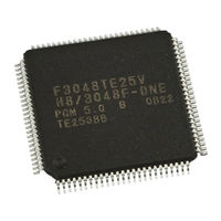
Renesas F-ZTAT H8/3048 Series Hardware Manual (905 pages)
16-Bit Single-Chip Microcomputer
Brand:
Renesas
| Category:
Computer Hardware
| Size: 8.58 MB
Table of Contents
Sample Program
7
Table of Contents
11
Section 1 Overview
25
Overview
25
Block Diagram
31
Pin Description
32
Pin Arrangement
32
Pin Assignments in each Mode
34
Pin Functions
39
Differences between H8/3048F and H8/3048F-ONE
44
Section 2 CPU
49
Overview
49
Features
49
Differences from H8/300 CPU
50
CPU Operating Modes
51
Address Space
52
Register Configuration
53
Overview
53
General Registers
54
Control Registers
55
Initial CPU Register Values
56
Data Formats
57
General Register Data Formats
57
Memory Data Formats
59
Instruction Set
60
Instruction Set Overview
60
Instructions and Addressing Modes
61
Tables of Instructions Classified by Function
62
Basic Instruction Formats
71
Notes on Use of Bit Manipulation Instructions
72
Addressing Modes and Effective Address Calculation
74
Addressing Modes
74
Effective Address Calculation
76
Processing States
80
Overview
80
Program Execution State
81
Exception-Handling State
81
Exception-Handling Sequences
83
Bus-Released State
84
Reset State
84
Power-Down State
84
Basic Operational Timing
85
Overview
85
On-Chip Memory Access Timing
85
On-Chip Supporting Module Access Timing
86
Access to External Address Space
87
Section 3 MCU Operating Modes
89
Overview
89
Operating Mode Selection
89
Register Configuration
90
Mode Control Register (MDCR)
90
System Control Register (SYSCR)
91
Operating Mode Descriptions
93
Mode 1
93
Mode 2
93
Mode 3
93
Mode 4
93
Mode 5
93
Mode 6
94
Mode 7
94
Pin Functions in each Operating Mode
94
Memory Map in each Operating Mode
95
Section 4 Exception Handling
105
Overview
105
Exception Handling Types and Priority
105
Exception Handling Operation
105
Exception Vector Table
106
Reset
108
Overview
108
Reset Sequence
108
Interrupts after Reset
111
Interrupts
112
Trap Instruction
113
Stack Status after Exception Handling
113
Notes on Stack Usage
114
Section 5 Interrupt Controller
115
Overview
115
Features
115
Block Diagram
116
Pin Configuration
117
Register Configuration
117
Register Descriptions
118
System Control Register (SYSCR)
118
Interrupt Priority Registers a and B (IPRA, IPRB)
119
IRQ Status Register (ISR)
126
IRQ Enable Register (IER)
127
IRQ Sense Control Register (ISCR)
128
Interrupt Sources
129
External Interrupts
129
Internal Interrupts
130
Interrupt Vector Table
130
Interrupt Operation
134
Interrupt Handling Process
134
Interrupt Sequence
139
Interrupt Response Time
140
Usage Notes
141
Contention between Interrupt and Interrupt-Disabling Instruction
141
Instructions that Inhibit Interrupts
142
Interrupts During EEPMOV Instruction Execution
142
Usage Notes on External Interrupts
142
Notes on Non-Maskable Interrupts (NMI)
144
Section 6 Bus Controller
147
Overview
147
Features
147
Block Diagram
148
Input/Output Pins
149
Register Configuration
150
Register Descriptions
150
Bus Width Control Register (ABWCR)
150
Access State Control Register (ASTCR)
151
Wait Control Register (WCR)
152
Wait State Controller Enable Register (WCER)
153
Bus Release Control Register (BRCR)
154
Chip Select Control Register (CSCR)
155
Operation
157
Area Division
157
Chip Select Signals
158
Data Bus
160
Bus Control Signal Timing
161
Wait Modes
169
Interconnections with Memory (Example)
175
Bus Arbiter Operation
177
Usage Notes
180
Connection to Dynamic RAM and Pseudo-Static RAM
180
Register Write Timing
180
BREQ Input Timing
182
Transition to Software Standby Mode
182
Section 7 Refresh Controller
183
Overview
183
Features
183
Block Diagram
184
Input/Output Pins
185
Register Configuration
185
Register Descriptions
186
Refresh Control Register (RFSHCR)
186
Refresh Timer Control/Status Register (RTMCSR)
189
Refresh Timer Counter (RTCNT)
190
Refresh Time Constant Register (RTCOR)
191
Operation
192
Overview
192
DRAM Refresh Control
194
Pseudo-Static RAM Refresh Control
209
Interval Timer
213
Interrupt Source
219
Usage Notes
219
Section 8 DMA Controller
221
Overview
221
Features
221
Block Diagram
222
Functional Overview
223
Input/Output Pins
225
Register Configuration
225
Register Descriptions (Short Address Mode)
227
Memory Address Registers (MAR)
227
I/O Address Registers (IOAR)
228
Execute Transfer Count Registers (ETCR)
229
Data Transfer Control Registers (DTCR)
230
Register Descriptions (Full Address Mode)
233
Memory Address Registers (MAR)
233
I/O Address Registers (IOAR)
233
Execute Transfer Count Registers (ETCR)
234
Data Transfer Control Registers (DTCR)
236
Operation
242
Overview
242
I/O Mode
244
Idle Mode
246
Repeat Mode
249
Normal Mode
253
Block Transfer Mode
256
DMAC Activation
261
DMAC Bus Cycle
263
DMAC Multiple-Channel Operation
269
External Bus Requests, Refresh Controller, and DMAC
270
NMI Interrupts and DMAC
271
Aborting a DMA Transfer
272
Exiting Full Address Mode
273
DMAC States in Reset State, Standby Modes, and Sleep Mode
274
Interrupts
275
Usage Notes
276
Note on Word Data Transfer
276
DMAC Self-Access
276
Longword Access to Memory Address Registers
276
Note on Full Address Mode Setup
276
Note on Activating DMAC by Internal Interrupts
276
NMI Interrupts and Block Transfer Mode
278
Memory and I/O Address Register Values
278
Bus Cycle When Transfer Is Aborted
279
Section 9 I/O Ports
281
Overview
281
Port 1
285
Overview
285
Register Descriptions
286
Port 2
288
Overview
288
Register Descriptions
289
Port 3
292
Overview
292
Register Descriptions
292
Port 4
294
Overview
294
Register Descriptions
295
Port 5
298
Overview
298
Register Descriptions
299
Port 6
302
Overview
302
Register Descriptions
303
Port 7
306
Overview
306
Register Description
307
Port 8
308
Overview
308
Register Descriptions
309
Port 9
313
Overview
313
Register Descriptions
314
Port a
318
Overview
318
Register Descriptions
320
Pin Functions
322
Port B
330
Overview
330
Register Descriptions
332
Pin Functions
334
Section 10 16-Bit Integrated Timer Unit (ITU)
339
Overview
339
Features
339
Block Diagrams
342
Input/Output Pins
347
Register Configuration
348
Register Descriptions
351
Timer Start Register (TSTR)
351
Timer Synchro Register (TSNC)
352
Timer Mode Register (TMDR)
354
Timer Function Control Register (TFCR)
357
Timer Output Master Enable Register (TOER)
359
Timer Output Control Register (TOCR)
361
Timer Counters (TCNT)
362
General Registers (GRA, GRB)
363
Buffer Registers (BRA, BRB)
364
Timer Control Registers (TCR)
365
Timer I/O Control Register (TIOR)
367
Timer Status Register (TSR)
369
Timer Interrupt Enable Register (TIER)
371
CPU Interface
373
16-Bit Accessible Registers
373
8-Bit Accessible Registers
375
Operation
376
Overview
376
Basic Functions
377
Synchronization
386
PWM Mode
388
Reset-Synchronized PWM Mode
392
Complementary PWM Mode
395
Phase Counting Mode
404
Buffering
406
ITU Output Timing
413
Interrupts
415
Setting of Status Flags
415
Clearing of Status Flags
417
Interrupt Sources and DMA Controller Activation
418
Usage Notes
419
Section 11 Programmable Timing Pattern Controller
435
Overview
435
Features
435
Block Diagram
436
TPC Pins
437
Registers
438
Register Descriptions
439
Port a Data Direction Register (PADDR)
439
Port a Data Register (PADR)
439
Port B Data Direction Register (PBDDR)
440
Port B Data Register (PBDR)
440
Next Data Register a (NDRA)
441
Next Data Register B (NDRB)
443
Next Data Enable Register a (NDERA)
445
Next Data Enable Register B (NDERB)
446
TPC Output Control Register (TPCR)
447
TPC Output Mode Register (TPMR)
449
Operation
451
Overview
451
Output Timing
452
Normal TPC Output
453
Non-Overlapping TPC Output
455
TPC Output Triggering by Input Capture
457
Usage Notes
458
Operation of TPC Output Pins
458
Note on Non-Overlapping Output
458
Section 12 Watchdog Timer
461
Overview
461
Features
461
Block Diagram
462
Pin Configuration
462
Register Configuration
463
Register Descriptions
463
Timer Counter (TCNT)
463
Timer Control/Status Register (TCSR)
464
Reset Control/Status Register (RSTCSR)
466
Notes on Register Access
467
Operation
469
Watchdog Timer Operation
469
Interval Timer Operation
470
Timing of Setting of Overflow Flag (OVF)
470
Timing of Setting of Watchdog Timer Reset Bit (WRST)
471
Interrupts
472
Usage Notes
472
Notes
473
Section 13 Serial Communication Interface
475
Overview
475
Features
475
Block Diagram
477
Input/Output Pins
478
Register Configuration
478
Register Descriptions
479
Receive Shift Register (RSR)
479
Receive Data Register (RDR)
479
Transmit Shift Register (TSR)
480
Transmit Data Register (TDR)
480
Serial Mode Register (SMR)
481
Serial Control Register (SCR)
484
Serial Status Register (SSR)
488
Bit Rate Register (BRR)
492
Operation
500
Overview
500
Operation
504
Operation in Asynchronous Mode
506
Multiprocessor Communication
515
Synchronous Operation
522
SCI Interrupts
526
Usage Notes
531
Section 14 Smart Card Interface
533
Overview
533
Features
533
Block Diagram
534
Input/Output Pins
535
Register Configuration
535
Register Descriptions
536
Smart Card Mode Register (SCMR)
536
Serial Status Register (SSR)
537
Serial Mode Register (SMR)
539
Serial Control Register (SCR)
540
Operation
541
Overview
541
Pin Connections
541
Data Format
543
Register Settings
544
Clock
546
Transmitting and Receiving Data
548
Usage Notes
555
Section 15 A/D Converter
559
Overview
559
Features
559
Block Diagram
560
Input Pins
561
Register Configuration
562
Register Descriptions
563
A/D Data Registers a to D (ADDRA to ADDRD)
563
A/D Control/Status Register (ADCSR)
564
A/D Control Register (ADCR)
566
CPU Interface
567
Operation
568
Single Mode (SCAN = 0)
568
Scan Mode (SCAN = 1)
570
Input Sampling and A/D Conversion Time
572
External Trigger Input Timing
573
Interrupts
574
Usage Notes
574
Section 16 D/A Converter
581
Overview
581
Features
581
Block Diagram
582
Input/Output Pins
583
Register Configuration
583
Register Descriptions
584
D/A Data Registers 0 and 1 (DADR0/1)
584
D/A Control Register (DACR)
584
D/A Standby Control Register (DASTCR)
586
Operation
587
D/A Output Control
588
Usage Notes
588
Section 17 RAM
589
Overview
589
Block Diagram
590
Register Configuration
590
System Control Register (SYSCR)
591
Operation
592
Section 18 ROM (H8/3048ZTAT and Mask-ROM Versions)
593
Overview
593
Block Diagram
594
PROM Mode
595
PROM Mode Setting
595
Socket Adapter and Memory Map
595
PROM Programming
597
Programming and Verification
598
Programming Precautions
602
Reliability of Programmed Data
603
Notes on Ordering Mask ROM Version Chip
604
Section 19 Flash Memory
607
Pp = 12 V))
607
Overview
607
Flash Memory Overview
608
Flash Memory Operation
608
Mode Programming and Flash Memory Address Space
609
Features
610
Block Diagram
611
Input/Output Pins
612
Register Configuration
612
Flash Memory Register Descriptions
613
Flash Memory Control Register
613
Erase Block Register 1
616
Erase Block Register 2
617
RAM Control Register (RAMCR)
619
On-Board Programming Modes
620
Boot Mode
621
User Program Mode
626
Programming and Erasing Flash Memory
628
Program Mode
629
Program-Verify Mode
629
Programming Flowchart and Sample Program
630
Erase Mode
633
Erase-Verify Mode
633
Erasing Flowchart and Sample Program
634
Prewrite-Verify Mode
648
Protect Modes
649
NMI Input Masking
652
Flash Memory Emulation by RAM
653
Flash Memory PROM Mode
655
PROM Mode Setting
655
Socket Adapter and Memory Map
656
Operation in PROM Mode
658
Flash Memory Programming and Erasing Precautions (Dual-Power Supply)
667
Notes When Converting the F-ZTAT (Dual-Power Supply) Application Software to the Mask-ROM Versions
675
Section 20 Clock Pulse Generator
677
Overview
677
Block Diagram
678
Oscillator Circuit
679
Connecting a Crystal Resonator
679
External Clock Input
681
Duty Adjustment Circuit
683
Prescalers
683
Frequency Divider
684
Register Configuration
684
Division Control Register (DIVCR)
684
Usage Notes
685
Section 21 Power-Down State
687
Overview
687
Register Configuration
689
System Control Register (SYSCR)
689
Module Standby Control Register (MSTCR)
691
Sleep Mode
693
Transition to Sleep Mode
693
Exit from Sleep Mode
693
Software Standby Mode
693
Transition to Software Standby Mode
693
Exit from Software Standby Mode
694
Selection of Waiting Time for Exit from Software Standby Mode
694
Sample Application of Software Standby Mode
696
Note
696
Hardware Standby Mode
697
Transition to Hardware Standby Mode
697
Exit from Hardware Standby Mode
697
Timing for Hardware Standby Mode
697
Module Standby Function
698
Module Standby Timing
698
Read/Write in Module Standby
698
Usage Notes
699
System Clock Output Disabling Function
700
Section 22 Electrical Characteristics
701
Electrical Characteristics for H8/3048 ZTAT (PROM) and On-Chip Mask ROM Versions
703
Absolute Maximum Ratings
703
DC Characteristics
704
AC Characteristics
710
A/D Conversion Characteristics
717
D/A Conversion Characteristics
718
Electrical Characteristics of H8/3048F (Dual-Power Supply)
719
Absolute Maximum Ratings
719
DC Characteristics
720
AC Characteristics
727
A/D Conversion Characteristics
733
D/A Conversion Characteristics
734
Flash Memory Characteristics
735
Operational Timing
736
Bus Timing
736
Refresh Controller Bus Timing
740
Control Signal Timing
745
Clock Timing
747
TPC and I/O Port Timing
747
ITU Timing
748
SCI Input/Output Timing
749
DMAC Timing
750
Appendix A Instruction Set
751
Instruction List
751
Data Transfer Instructions
753
Arithmetic Instructions
755
Bit Manipulation Instructions
760
Operation Code Map
766
Number of States Required for Execution
769
Appendix B Internal I/O Register
779
Addresses
780
B.1 Addresses
780
B.2 Function
788
Appendix C I/O Port Block Diagrams
868
C.2 Port 2 Block Diagram
869
C.3 Port 3 Block Diagram
870
C.4 Port 4 Block Diagram
871
C.5 Port 5 Block Diagram
872
C.6 Port 6 Block Diagrams
873
C.7 Port 7 Block Diagrams
877
C.8 Port 8 Block Diagrams
878
C.9 Port 9 Block Diagrams
881
C.10 Port a Block Diagrams
885
C.11 Port B Block Diagrams
889
Appendix D Pin States
893
D.2 Pin States at Reset
896
Appendix F Product Code Lineup
900
Appendix G Package Dimensions
901
Advertisement
Renesas F-ZTAT H8/3048 Series User Manual (34 pages)
User System Interface Cable
Brand:
Renesas
| Category:
Computer Hardware
| Size: 0.37 MB
Table of Contents
Important Information
7
Limited Warranty
8
Table of Contents
14
Section 1 Configuration
15
Section 2 Connection Procedures
17
Connecting User System Interface Cable to Emulator Station
17
Connecting User System Interface Cable to User System
19
Installing IC Socket
19
Soldering IC Socket
19
Inserting Cable Head
20
Fastening Cable Head
20
Fastening Cable Body
22
Recommended Dimensions for User System Mount Pad
23
Dimensions for User System Interface Cable Head
24
Resulting Dimensions after Connecting User System Interface Cable
25
Section 3 Installing the MCU to the User System
26
Section 4 Verifying Operation
28
Section 5 Notice
29
Advertisement
Related Products
Renesas H8/3007
Renesas H8/3062
Renesas H8/3052
Renesas H8/3067
Renesas H8/300H Series
Renesas F-ZTAT H8/3052B Series
Renesas F-ZTAT H8/3067F
Renesas F-ZTAT H8/3039F
Renesas H8/300 Series
Renesas H8/3066
Renesas Categories
Computer Hardware
Motherboard
Microcontrollers
Adapter
Switch
More Renesas Manuals
Login
Sign In
OR
Sign in with Facebook
Sign in with Google
Upload manual
Upload from disk
Upload from URL