Sign In
Upload
Manuals
Brands
Renesas Manuals
Microcontrollers
RL78/G1P
Renesas RL78/G1P Manuals
Manuals and User Guides for Renesas RL78/G1P. We have
5
Renesas RL78/G1P manuals available for free PDF download: Hardware User Manual, User Manual
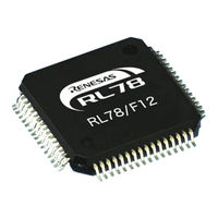
Renesas RL78/G1P Hardware User Manual (770 pages)
16-Bit Single-Chip Microcontroller
Brand:
Renesas
| Category:
Microcontrollers
| Size: 7 MB
Table of Contents
Table of Contents
7
Chapter 1 Outline
20
Features
20
List of Part Numbers
22
Pin Configuration (Top View)
23
24-Pin Products
23
32-Pin Products
24
Pin Identification
25
Block Diagram
26
24-Pin Products
26
32-Pin Products
27
Outline of Functions
28
Chapter 2 Pin Functions
30
Pin Function List
30
24-Pin Products
31
32-Pin Products
32
Functions Other than Port Pins
33
With Functions for each Product
33
Function Descriptions
34
Description of Pin Functions
36
P10 to P17 (Port 1)
36
P20 to P27 (Port 2)
36
P30 to P35 (Port 3)
37
P40 (Port 4)
38
P60, P61 (Port 6)
39
P121, P122 (Port 12)
39
P137 (Port 13)
40
VDD , Vss
40
Reset
40
Regc
40
Connection of Unused Pins
41
Chapter 3 Cpu Architecture
44
Memory Space
44
Internal Program Memory Space
48
Mirror Area
50
Internal Data Memory Space
52
Special Function Register (SFR) Area
52
Extended Special Function Register (2Nd SFR: 2Nd Special Function Register) Area
52
Data Memory Addressing
53
Processor Registers
54
Control Registers
54
General-Purpose Registers
56
And CS Registers
57
Special Function Registers (Sfrs)
58
Extended Special Function Registers (2Nd Sfrs: 2Nd Special Function Registers)
62
Instruction Address Addressing
67
Relative Addressing
67
Immediate Addressing
67
Register Indirect Addressing
68
Addressing for Processing Data Addresses
69
Implied Addressing
69
Register Addressing
69
Direct Addressing
70
Short Direct Addressing
71
SFR Addressing
72
Register Indirect Addressing
73
Based Addressing
74
Based Indexed Addressing
78
Stack Addressing
79
Chapter 4 Port Functions
83
Port Functions
83
Port Configuration
83
Port 12
83
Port 1
84
Port 2
89
Port 3
92
Port 4
98
Port 6
99
Port 13
101
Registers Controlling Port Function
102
Port Mode Registers (Pmxx)
104
Port Registers (Pxx)
105
Pull-Up Resistor Option Registers (Puxx)
106
Port Mode Control Register 1 (PMC1) (24-Pin Products Only)
107
A/D Port Configuration Register (ADPC)
108
Port Function Operations
109
Writing to I/O Port
109
Reading from I/O Port
109
Operations on I/O Port
109
Settings of Port Related Register When Using Alternate Function
110
Cautions When Using Port Function
113
Cautions on 1-Bit Manipulation Instruction for Port Register N (Pn)
113
Cautions on Specifying the Pin Settings
114
Chapter 5 Clock Generator
115
Functions of Clock Generator
115
Configuration of Clock Generator
116
Registers Controlling Clock Generator
118
Clock Operation Mode Control Register (CMC)
118
System Clock Control Register (CKC)
120
Clock Operation Status Control Register (CSC)
121
Oscillation Stabilization Time Counter Status Register (OSTC)
122
Oscillation Stabilization Time Select Register (OSTS)
124
Peripheral Enable Registers 0, 1 (PER0, PER1)
126
High-Speed On-Chip Oscillator Frequency Select Register (HOCODIV)
128
High-Speed On-Chip Oscillator Trimming Register (HIOTRM)
129
System Clock Oscillator
130
X1 Oscillator
130
High-Speed On-Chip Oscillator
133
Low-Speed On-Chip Oscillator
133
Clock Generator Operation
134
Controlling Clock
136
Example of Setting High-Speed On-Chip Oscillator
136
Example of Setting X1 Oscillation Clock
137
CPU Clock Status Transition Diagram
138
Condition before Changing CPU Clock and Processing after Changing CPU Clock
142
Time Required for Switchover of CPU Clock and System Clock
143
Preconditions for Stopping Clock Oscillation
143
Resonator and Oscillator Constants
144
Chapter 6 Timer Array Unit
145
Functions of Timer Array Unit
147
Independent Channel Operation Function
147
Simultaneous Channel Operation Function
148
8-Bit Timer Operation Function (Channels 1 and 3 Only)
149
Configuration of Timer Array Unit
150
Timer Count Register Mn (Tcrmn)
154
Timer Data Register Mn (Tdrmn)
155
Registers Controlling Timer Array Unit
156
Peripheral Enable Register 0 (PER0)
157
Timer Clock Select Register M (Tpsm)
158
Timer Mode Register Mn (Tmrmn)
161
Timer Status Register Mn (Tsrmn)
166
Timer Channel Enable Status Register M (Tem)
167
Timer Channel Start Register M (Tsm)
168
Timer Channel Stop Register M (Ttm)
169
Timer Input Select Register 0 (TIS0)
170
Timer Output Enable Register M (Toem)
171
Timer Output Register M (Tom)
172
Timer Output Level Register M (Tolm)
173
Timer Output Mode Register M (Tomm)
174
Noise Filter Enable Register 1 (NFEN1)
175
Port Mode Registers 1, 3 ( PM1, PM3)
176
Basic Rules of Timer Array Unit
177
Basic Rules of Simultaneous Channel Operation Function
177
Basic Rules of 8-Bit Timer Operation Function (Channels 1 and 3 Only)
179
Operation of Counter
180
Count Clock (F )
180
Start Timing of Counter
182
Operation of Counter
183
Channel Output (Tomn Pin) Control
188
Tomn Pin Output Circuit Configuration
188
Tomn Pin Output Setting
189
Cautions on Channel Output Operation
190
Collective Manipulation of Tomn Bit
195
Timer Interrupt and Tomn Pin Output at Operation Start
196
Timer Input (Timn) Control
197
Timn Input Circuit Configuration
197
Noise Filter
197
Cautions on Channel Input Operation
198
Independent Channel Operation Function of Timer Array Unit
199
Operation as Interval Timer/Square Wave Output
199
Operation as External Event Counter
205
Operation as Input Pulse Interval Measurement
210
Operation as Input Signal High-/Low-Level Width Measurement
214
Operation as Delay Counter
218
Simultaneous Channel Operation Function of Timer Array Unit
223
Operation as One-Shot Pulse Output Function
223
Operation as PWM Function
230
Operation as Multiple PWM Output Function
237
Cautions When Using Timer Array Unit
245
Cautions When Using Timer Output
245
Chapter 7 Clock Output/Buzzer Output Controller
246
Functions of Clock Output/Buzzer Output Controller
246
Configuration of Clock Output/Buzzer Output Controller
248
Registers Controlling Clock Output/Buzzer Output Controller
248
Clock Output Select Registers N (Cksn)
248
Registers Controlling Port Functions of Pins to be Used for Clock or Buzzer Output
250
Operations of Clock Output/Buzzer Output Controller
251
Operation as Output Pin
251
Cautions of Clock Output/Buzzer Output Controller
251
Chapter 8 Watchdog Timer
252
Functions of Watchdog Timer
252
Configuration of Watchdog Timer
253
Register Controlling Watchdog Timer
254
Watchdog Timer Enable Register (WDTE)
254
Operation of Watchdog Timer
255
Controlling Operation of Watchdog Timer
255
Setting Overflow Time of Watchdog Timer
256
Setting Window Open Period of Watchdog Timer
257
Setting Watchdog Timer Interval Interrupt
259
Chapter 9 A/D Converter
260
Function of A/D Converter
260
Configuration of A/D Converter
263
Registers Controlling A/D Converter
265
Peripheral Enable Register 0 (PER0)
266
A/D Converter Mode Register 0 (ADM0)
267
A/D Converter Mode Register 1 (ADM1)
276
A/D Converter Mode Register 2 (ADM2)
277
12-Bit A/D Conversion Result Register (ADCR)
280
8-Bit A/D Conversion Result Register (ADCRH)
281
Analog Input Channel Specification Register (ADS)
282
Conversion Result Comparison Upper Limit Setting Register (ADUL)
284
Conversion Result Comparison Lower Limit Setting Register (ADLL)
284
A/D Test Register (ADTES)
285
Registers Controlling Port Function of Analog Input Pins
286
A/D Converter Conversion Operations
287
Input Voltage and Conversion Results
289
A/D Converter Operation Modes
290
Software Trigger Mode (Select Mode, Sequential Conversion Mode)
290
Software Trigger Mode (Select Mode, One-Shot Conversion Mode)
291
Software Trigger Mode (Scan Mode, Sequential Conversion Mode)
292
Software Trigger Mode (Scan Mode, One-Shot Conversion Mode)
293
Hardware Trigger No-Wait Mode (Select Mode, Sequential Conversion Mode)
294
Hardware Trigger No-Wait Mode (Select Mode, One-Shot Conversion Mode)
295
Hardware Trigger No-Wait Mode (Scan Mode, Sequential Conversion Mode)
296
Hardware Trigger No-Wait Mode (Scan Mode, One-Shot Conversion Mode)
297
Hardware Trigger Wait Mode (Select Mode, Sequential Conversion Mode)
298
Hardware Trigger Wait Mode (Select Mode, One-Shot Conversion Mode)
299
Hardware Trigger Wait Mode (Scan Mode, Sequential Conversion Mode)
300
Hardware Trigger Wait Mode (Scan Mode, One-Shot Conversion Mode)
301
A/D Converter Setup Flowchart
302
Setting up Software Trigger Mode
303
Setting up Hardware Trigger No-Wait Mode
304
Setting up Hardware Trigger Wait Mode
305
Setup When Temperature Sensor Output Voltage/Internal Reference Voltage Is Selected
306
(Example for Software Trigger Mode and One-Shot Conversion Mode)
306
Setting up Test Mode
307
SNOOZE Mode Function
308
How to Read A/D Converter Characteristics Table
312
Cautions for A/D Converter
314
Chapter 10 D/A Converter
318
Function of D/A Converter
318
Configuration of D/A Converter
319
Configuration of A/D Converter
320
A/D Port Configuration Register (ADPC)
320
Peripheral Enable Register 1 (PER1)
321
D/A Converter Mode Register (DAM)
322
D/A Conversion Value Setting Register I (Dacsi) (I = 0, 1)
322
Port Mode Register 2 (PM2)
323
Operations of D/A Converter
324
Operation in Normal Mode
324
Operation in Real-Time Output Mode
325
Cautions for D/A Converter
326
Chapter 11 Serial Array Unit
327
Functions of Serial Array Unit
328
3-Wire Serial I/O (CSI00)
328
Uart (Uart0)
329
Configuration of Serial Array Unit
330
Shift Register
332
Lower 8/9 Bits of the Serial Data Register Mn (Sdrmn)
332
Registers Controlling Serial Array Unit
334
Peripheral Enable Register 0 (PER0)
335
Serial Clock Select Register M (Spsm)
336
Serial Mode Register Mn (Smrmn)
337
Serial Communication Operation Setting Register Mn (Scrmn)
338
Higher 7 Bits of the Serial Data Register Mn (Sdrmn)
341
Serial Flag Clear Trigger Register Mn (Sirmn)
342
Serial Status Register Mn (Ssrmn)
343
Serial Channel Start Register M (Ssm)
345
Serial Channel Stop Register M (Stm)
346
Serial Channel Enable Status Register M (Sem)
347
Serial Output Enable Register M (Soem)
348
Serial Output Register M (Som)
349
Serial Output Level Register M (Solm)
350
Serial Standby Control Register M (Sscm)
351
Input Switch Control Register (ISC)
352
Noise Filter Enable Register 0 (NFEN0)
353
Port Mode Register 3 (PM3)
354
Operation Stop Mode
355
Stopping the Operation by Units
356
Stopping the Operation by Channels
357
Operation of 3-Wire Serial I/O (CSI00) Communication
358
Master Transmission
360
Master Reception
369
Master Transmission/Reception
378
Slave Transmission
387
Slave Reception
396
Slave Transmission/Reception
402
SNOOZE Mode Function (CSI00)
411
Calculating Transfer Clock Frequency
415
Procedure for Processing Errors that Occurred During 3-Wire Serial I/O (CSI00)
417
Communication
417
Clock Synchronous Serial Communication with Slave Select Input Function
418
Slave Transmission
421
Advertisement
Renesas RL78/G1P User Manual (59 pages)
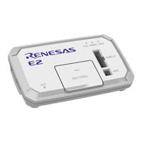
Emulator
Brand:
Renesas
| Category:
Computer Hardware
| Size: 1 MB
Table of Contents
Table of Contents
4
Overview
7
Overview of E1/E20/E2 Emulator and E2 Emulator Lite
7
Note on Using E20
7
Configuration of E1/E20/E2/E2 Lite Manuals
8
Supported Devices
9
Overview of the Specifications of the External Trigger Input and Output
11
Assignments of the External Trigger Input and Output Pins
11
Specifications of the External Trigger Inputs and Outputs
12
Designing the User System
13
Connecting the E1/E20/E2/E2 Lite to the User System
13
Installing the Connector on the User System
13
Connecting the User System Interface Cable to the 14-Pin Connector
13
Pin Assignments of the Connector on the User System
17
14-Pin Connector Specifications
17
Recommended Circuits between the Connector and the MCU
19
Connection between the 14-Pin Connector and the RL78 Family Mcus in General
19
Connection between the 14-Pin Connector and the RL78 Family Mcus
21
And the 20- and 24-Pin Versions of the RL78/G12)
21
Connection between the 14-Pin Connector and the RL78 Family MCU (Only the RL78/I1C)
22
Notes on Connection
25
RESET# Pin
25
TOOL0 Pin
28
Gnd
29
VDD
29
Internal Circuits of the Emulator
31
Internal Circuits of the E1 (When the RL78 Family Is Connected)
31
Internal Circuits of the E20 (When the RL78 Family Is Connected)
32
Internal Circuits of the E2 (When the RL78 Family Is Connected)
33
Internal Circuits of the E2 Lite (When the RL78 Family Is Connected)
35
Notes on Designing the User System
36
Isolator for the E1
36
Small Connector Conversion Adapter for the E1
36
Notes on Usage
38
Turning the Power On/Off
38
When a Separate Power Supply Is Used for the User System
38
When Power Is Supplied to the User System from the Emulator (E1/E2/E2 Lite Only)
39
Power Supply Function of the E1/E2/E2 Lite
39
MCU Resources to be Occupied
40
Securing an Area for the Debugging Monitor Program
41
Securing a Stack Area for Debugging
42
Setting an On-Chip Debugging Option Byte
43
Setting a Security ID
44
Setting a Serial Programming Security ID
45
Reset
46
Operation after a Reset
46
SP Value after a Reset
46
Flash Memory
46
Flash Memory Programming by Self-Programming
46
Operation for Voltages and Flash Operation Modes Not Permitting Flash Memory Rewriting
47
Gdidis
47
RESET# Multiplexed Pin
47
Mcus that Are Used in Debugging
48
Usage in Mass-Production
48
Standalone Operation
48
Final Evaluation of the User Program
48
Debug Functions
49
Stepped Execution
49
Go to Here]
49
Debugging in Standby Mode
49
Pseudo-Real-Time RAM Monitor Function or Pseudo-Dynamic Memory Modification Function
50
Start/Stop Functions
50
Emulation of Flash Memory CRC Accumulator Function
51
Break Function
51
Setting and Deleting Events During User Program Execution
51
Trace Function
51
Battery Backup Function
51
RAM-ECC Function
51
Extended Functions of the E2
52
Points for Caution on Using the Rl78/G2X
52
Points for Caution on Using the Rl78/F2X
54
Note on Self-Programming for Flash-Memory
56
State of High-Speed on Chip Oscillator During On-Chip Debugging
56
Setting of Download Mode (RL78/FGIC[RAJ240100])
56
Renesas RL78/G1P User Manual (58 pages)
E1/E20/E2 Emulator, E2 Emulator Lite
Brand:
Renesas
| Category:
Computer Hardware
| Size: 0 MB
Table of Contents
Table of Contents
4
Overview
7
Overview of E1/E20/E2 Emulator and E2 Emulator Lite
7
Note on Using E20
7
Configuration of E1/E20/E2/E2 Lite Manuals
8
Supported Devices
9
Overview of the Specifications of the External Trigger Input and Output
11
Assignments of the External Trigger Input and Output Pins
11
Specifications of the External Trigger Inputs and Outputs
12
Designing the User System
13
Connecting the E1/E20/E2/E2 Lite to the User System
13
Installing the Connector on the User System
13
Connecting the User System Interface Cable to the 14-Pin Connector
13
Pin Assignments of the Connector on the User System
17
14-Pin Connector Specifications
17
Recommended Circuits between the Connector and the MCU
19
Connection between the 14-Pin Connector and the RL78 Family Mcus in General
19
Connection between the 14-Pin Connector and the RL78 Family Mcus (Only the RL78/G11 and the 20- and 24-Pin Versions of the RL78/G12)
21
Connection between the 14-Pin Connector and the RL78 Family MCU (Only the RL78/I1C)
22
Notes on Connection
25
RESET# Pin
25
TOOL0 Pin
28
Gnd
29
VDD
29
Internal Circuits of the Emulator
31
Internal Circuits of the E1 (When the RL78 Family Is Connected)
31
Internal Circuits of the E20 (When the RL78 Family Is Connected)
32
Internal Circuits of the E2 (When the RL78 Family Is Connected)
33
Internal Circuits of the E2 Lite (When the RL78 Family Is Connected)
35
Notes on Designing the User System
36
Isolator for the E1
36
Small Connector Conversion Adapter for the E1
36
Notes on Usage
38
Turning the Power On/Off
38
When a Separate Power Supply Is Used for the User System
38
When Power Is Supplied to the User System from the Emulator (E1/E2/E2 Lite Only)
39
Power Supply Function of the E1/E2/E2 Lite
39
MCU Resources to be Occupied
40
Securing an Area for the Debugging Monitor Program
41
Securing a Stack Area for Debugging
42
Setting an On-Chip Debugging Option Byte
43
Setting a Security ID
44
Setting a Serial Programming Security ID
45
Reset
46
Operation after a Reset
46
SP Value after a Reset
46
Flash Memory
46
Flash Memory Programming by Self-Programming
46
Operation for Voltages and Flash Operation Modes Not Permitting Flash Memory Rewriting
47
Gdidis
47
RESET# Multiplexed Pin
47
Mcus that Are Used in Debugging
48
Usage in Mass-Production
48
Standalone Operation
48
Final Evaluation of the User Program
48
Debug Functions
49
Stepped Execution
49
Go to Here]
49
Debugging in Standby Mode
49
Pseudo-Real-Time RAM Monitor Function or Pseudo-Dynamic Memory Modification Function
50
Start/Stop Functions
50
Emulation of Flash Memory CRC Accumulator Function
51
Break Function
51
Setting and Deleting Events During User Program Execution
51
Trace Function
51
Battery Backup Function
51
RAM-ECC Function
51
Extended Functions of the E2
52
Points for Caution on Using the RL78/G23
52
Points for Caution on Using the RL78/F24
54
Advertisement
Renesas RL78/G1P User Manual (55 pages)
Brand:
Renesas
| Category:
Computer Hardware
| Size: 0 MB
Table of Contents
Table of Contents
4
1 Overview
7
Overview of E1/E20/E2 Emulator and E2 Emulator Lite
7
Note on Using E20
7
Configuration of E1/E20/E2/E2 Lite Manuals
8
Supported Devices
9
Overview of the Specifications of the External Trigger Input and Output
11
Assignments of the External Trigger Input and Output Pins
11
Specifications of the External Trigger Inputs and Outputs
12
2 Designing the User System
13
Connecting the E1/E20/E2/E2 Lite to the User System
13
Installing the Connector on the User System
13
Connecting the User System Interface Cable to the 14-Pin Connector
13
Pin Assignments of the Connector on the User System
17
14-Pin Connector Specifications
17
Recommended Circuits between the Connector and the MCU
19
Connection between the 14-Pin Connector and the RL78 Family Mcus in General
19
Connection between the 14-Pin Connector and the RL78 Family Mcus (Only the RL78/G11 and the 20- and 24-Pin Versions of the RL78/G12)
21
Connection between the 14-Pin Connector and the RL78 Family MCU (Only the RL78/I1C)
22
Notes on Connection
25
RESET# Pin
25
TOOL0 Pin
28
Gnd
29
VDD
29
Internal Circuits of the Emulator
31
Internal Circuits of the E1 (When the RL78 Family Is Connected)
31
Internal Circuits of the E20 (When the RL78 Family Is Connected)
32
Internal Circuits of the E2 (When the RL78 Family Is Connected)
33
Internal Circuits of the E2 Lite (When the RL78 Family Is Connected)
35
Notes on Designing the User System
36
Isolator for the E1
36
Small Connector Conversion Adapter for the E1
36
3 Notes on Usage
38
Turning the Power On/Off
38
When a Separate Power Supply Is Used for the User System
38
When Power Is Supplied to the User System from the Emulator (E1/E2/E2 Lite Only)
39
Power Supply Function of the E1/E2/E2 Lite
39
MCU Resources to be Occupied
40
Securing an Area for the Debugging Monitor Program
41
Securing a Stack Area for Debugging
42
Setting an On-Chip Debugging Option Byte
43
Setting a Security ID
44
Reset
45
Operation after a Reset
45
SP Value after a Reset
45
Flash Memory
45
Flash Memory Programming by Self-Programming
45
Operation for Voltages and Flash Operation Modes Not Permitting Flash Memory Rewriting
46
Gdidis
46
RESET# Multiplexed Pin
46
Mcus that Are Used in Debugging
47
Usage in Mass-Production
47
Standalone Operation
47
Final Evaluation of the User Program
47
Debug Functions
48
Stepped Execution
48
Go to Here]
48
Debugging in Standby Mode
48
Pseudo-Real-Time RAM Monitor Function or Pseudo-Dynamic Memory Modification Function
49
Start/Stop Functions
49
Emulation of Flash Memory CRC Accumulator Function
50
Break Function
50
Setting and Deleting Events During User Program Execution
50
Trace Function
50
3.10.10 Battery Backup Function
50
3.10.11 RAM-ECC Function
50
3.10.12 Extended Functions of the E2
51
3.10.13 Points for Caution on Using the RL78/G23
51
Renesas RL78/G1P User Manual (27 pages)
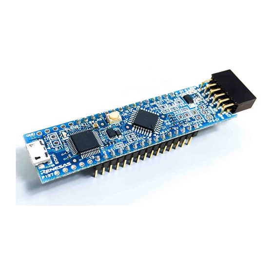
Fast Prototyping Board 16-Bit Single-Chip Microcontrollers
Brand:
Renesas
| Category:
Microcontrollers
| Size: 0 MB
Table of Contents
Table of Contents
6
1 Overview
7
Package Components
7
Purpose
7
Features
7
Preparation
7
RL78/G1P Fast Prototyping Board: Table of Specifications
8
Block Diagram
9
2 Board Layout
10
3 Parts Layout
11
4 Operating Environment
12
5 User Circuits
13
Rl78/G1P
13
USB Connector
13
Act Led
13
Power LED
13
User LED
13
Pmod Connector
14
Arduino Nano Connector
15
MCU Headers
17
Clock
17
Reset Switch
17
Emulator Reset Header
18
External Power-Supply Header
19
Current Measurement Header
20
6 Handling Precautions
21
Power to be Supplied
21
Remodeling the Board
21
Limitation on the Number of Connected RL78/G1P Fast Prototyping Boards
21
Power-Supply Circuits and Usage Conditions
21
7 Developing Code
22
Using the E 2 Studio
22
Using CS
23
8 Additional Information
24
Advertisement
Related Products
Renesas RL78/G13
Renesas RL78/G10
Renesas RL78/G1A
Renesas rl78/g1g
Renesas RL78/G1H
Renesas RL78/G1M
Renesas RL78/G1N
Renesas RL78/G23-128p
Renesas RL78/G15
Renesas RL78/F13
Renesas Categories
Computer Hardware
Motherboard
Microcontrollers
Adapter
Switch
More Renesas Manuals
Login
Sign In
OR
Sign in with Facebook
Sign in with Google
Upload manual
Upload from disk
Upload from URL