Sign In
Upload
Manuals
Brands
Renesas Manuals
Microcontrollers
RL78/G13
Renesas RL78/G13 Microcontrollers Manuals
Manuals and User Guides for Renesas RL78/G13 Microcontrollers. We have
12
Renesas RL78/G13 Microcontrollers manuals available for free PDF download: User Manual, Manual, Operation, Application Note, Hardware Manual
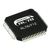
Renesas RL78/G13 User Manual (1092 pages)
16-Bit Single-Chip Microcontrollers
Brand:
Renesas
| Category:
Microcontrollers
| Size: 7 MB
Table of Contents
Table of Contents
7
Chapter 1 Outline
20
Features
20
Ordering Information
22
Pin Configuration (Top View)
25
20-Pin Products
25
24-Pin Products
26
25-Pin Products
27
30-Pin Products
28
32-Pin Products
29
36-Pin Products
30
40-Pin Products
31
44-Pin Products
32
48-Pin Products
33
52-Pin Products
35
64-Pin Products
36
80-Pin Products
38
100-Pin Products
39
128-Pin Products
41
Pin Identification
42
Block Diagram
43
20-Pin Products
43
24-Pin Products
44
25-Pin Products
45
30-Pin Products
46
32-Pin Products
47
36-Pin Products
48
40-Pin Products
49
44-Pin Products
50
48-Pin Products
51
52-Pin Products
52
64-Pin Products
53
80-Pin Products
54
100-Pin Products
55
128-Pin Products
56
Outline of Functions
57
Chapter 2 Pin Functions
63
Pin Function List
63
20-Pin Products
64
24-Pin Products
65
25-Pin Products
66
30-Pin Products
67
32-Pin Products
69
36-Pin Products
71
40-Pin Products
73
44-Pin Products
75
48-Pin Products
77
52-Pin Products
79
64-Pin Products
81
80-Pin Products
83
100-Pin Products
86
128-Pin Products
89
Pins for each Product (Pins Other than Port Pins)
93
Description of Pin Functions
99
P00 to P07 (Port 0)
99
P10 to P17 (Port 1)
100
P20 to P27 (Port 2)
101
P30 to P37 (Port 3)
101
P40 to P47 (Port 4)
102
P50 to P57 (Port 5)
104
P60 to P67 (Port 6)
104
P70 to P77 (Port 7)
105
P80 to P87 (Port 8)
106
P90 to P97 (Port 9)
106
P100 to P106 (Port 10)
106
P110 to P117 (Port 11)
107
P120 to P127 (Port 12)
107
P130, P137 (Port 13)
108
P140 to P147 (Port 14)
108
P150 to P156 (Port 15)
110
VDD , Ev Dd0 , Ev Dd1 , V Ss , Ev Ss0 , Ev Ss1
110
Reset
110
Regc
110
Pin I/O Circuits and Recommended Connection of Unused Pins
111
Chapter 3 Cpu Architecture
117
Memory Space
117
Internal Program Memory Space
133
Mirror Area
136
Internal Data Memory Space
138
Special Function Register (SFR) Area
139
Extended Special Function Register (2Nd SFR: 2Nd Special Function Register) Area
139
Data Memory Addressing
140
Processor Registers
150
Control Registers
150
General-Purpose Registers
152
ES and CS Registers
154
Special Function Registers (Sfrs)
155
Extended Special Function Registers (2Nd Sfrs: 2Nd Special Function Registers)
161
Instruction Address Addressing
170
Relative Addressing
170
Immediate Addressing
170
Table Indirect Addressing
171
Register Direct Addressing
172
Addressing for Processing Data Addresses
173
Implied Addressing
173
Register Addressing
173
Direct Addressing
174
Short Direct Addressing
175
SFR Addressing
176
Register Indirect Addressing
177
Based Addressing
178
Based Indexed Addressing
181
Stack Addressing
182
Chapter 4 Port Functions
183
Port Functions
183
Port Configuration
184
Port 0
186
Port 1
194
Port 2
204
Port 3
206
Port 4
211
Port 5
220
Port 6
227
Port 7
230
Port 8
237
Port 9
241
Port 10
246
Port 11
250
Port 12
250
Port 13
258
Port 14
260
Port 15
268
Registers Controlling Port Function
270
Port Function Operations
289
Writing to I/O Port
289
Reading from I/O Port
289
Operations on I/O Port
289
Connecting to External Device with Different Potential (1.8 V, 2.5 V, 3 V)
290
Settings of Port Mode Register, and Output Latch When Using Alternate Function
292
Cautions When Using Port Function
298
Cautions on 1-Bit Manipulation Instruction for Port Register N (Pn)
298
Cautions on the Pin Settings on the Products Other than 128-Pin
299
Chapter 5 Clock Generator
301
Functions of Clock Generator
301
Configuration of Clock Generator
303
Registers Controlling Clock Generator
305
System Clock Oscillator
321
X1 Oscillator
321
XT1 Oscillator
321
High-Speed On-Chip Oscillator
325
Low-Speed On-Chip Oscillator
325
Clock Generator Operation
326
Controlling Clock
328
Example of Setting High-Speed On-Chip Oscillator
328
Example of Setting X1 Oscillation Clock
329
Example of Setting XT1 Oscillation Clock
330
CPU Clock Status Transition Diagram
331
Condition before Changing CPU Clock and Processing after Changing CPU Clock
337
Time Required for Switchover of CPU Clock and Main System Clock
339
Conditions before Clock Oscillation Is Stopped
340
Chapter 6 Timer Array Unit
341
Functions of Timer Array Unit
343
Independent Channel Operation Function
343
Simultaneous Channel Operation Function
344
8-Bit Timer Operation Function (Channels 1 and 3 Only)
345
LIN-Bus Supporting Function (Channel 7 of Unit 0 Only)
346
Configuration of Timer Array Unit
347
Registers Controlling Timer Array Unit
353
Basic Rules of Timer Array Unit
378
Basic Rules of Simultaneous Channel Operation Function
378
Basic Rules of 8-Bit Timer Operation Function (Channels 1 and 3 Only)
380
Operation Timing of Counter
381
Count Clock (Ftclk)
381
Start Timing of Counter
383
Channel Output (Tomn Pin) Control
389
Tomn Pin Output Circuit Configuration
389
Tomn Pin Output Setting
390
Cautions on Channel Output Operation
391
Collective Manipulation of Tomn Bit
397
Timer Interrupt and Tomn Pin Output at Operation Start
398
Independent Channel Operation Function of Timer Array Unit
399
Operation as Interval Timer/Square Wave Output
399
Operation as External Event Counter
405
Operation as Frequency Divider (Channel 0 of Unit 0 Only)
410
Operation as Input Pulse Interval Measurement
414
Operation as Input Signal High-/Low-Level Width Measurement
418
Operation as Delay Counter
422
Simultaneous Channel Operation Function of Timer Array Unit
427
Operation as One-Shot Pulse Output Function
427
Operation as PWM Function
434
Operation as Multiple PWM Output Function
441
Cautions When Using Timer Array Unit
449
Cautions When Using Timer Output
449
Chapter 7 Real-Time Clock
450
Functions of Real-Time Clock
450
Configuration of Real-Time Clock
450
Registers Controlling Real-Time Clock
452
Real-Time Clock Operation
467
Starting Operation of Real-Time Clock
467
Shifting to STOP Mode after Starting Operation
468
Reading/Writing Real-Time Clock
469
Setting Alarm of Real-Time Clock
471
Hz Output of Real-Time Clock
472
Example of Watch Error Correction of Real-Time Clock
473
Chapter 8 Interval Timer
476
Functions of Interval Timer
476
Configuration of Interval Timer
476
Registers Controlling Interval Timer
477
Interval Timer Operation
480
Chapter 9 Clock Output/Buzzer Output Controller
481
Functions of Clock Output/Buzzer Output Controller
481
Configuration of Clock Output/Buzzer Output Controller
483
Registers Controlling Clock Output/Buzzer Output Controller
483
Operations of Clock Output/Buzzer Output Controller
486
Operation as Output Pin
486
Chapter 10 Watchdog Timer
487
Functions of Watchdog Timer
487
Configuration of Watchdog Timer
488
Register Controlling Watchdog Timer
489
Operation of Watchdog Timer
490
Controlling Operation of Watchdog Timer
490
Setting Overflow Time of Watchdog Timer
491
Setting Window Open Period of Watchdog Timer
492
Setting Watchdog Timer Interval Interrupt
493
Chapter 11 A/D Converter
494
Function of A/D Converter
494
Configuration of A/D Converter
496
Registers Used in A/D Converter
498
A/D Converter Conversion Operations
523
Input Voltage and Conversion Results
525
A/D Converter Operation Modes
526
Software Trigger Mode (Select Mode, Sequential Conversion Mode)
526
Software Trigger Mode (Select Mode, One-Shot Conversion Mode)
527
Software Trigger Mode (Scan Mode, Sequential Conversion Mode)
528
Software Trigger Mode (Scan Mode, One-Shot Conversion Mode)
529
Hardware Trigger No-Wait Mode (Select Mode, Sequential Conversion Mode)
530
Hardware Trigger No-Wait Mode (Select Mode, One-Shot Conversion Mode)
531
Hardware Trigger No-Wait Mode (Scan Mode, Sequential Conversion Mode)
532
Hardware Trigger No-Wait Mode (Scan Mode, One-Shot Conversion Mode)
533
Hardware Trigger Wait Mode (Select Mode, Sequential Conversion Mode)
534
Hardware Trigger Wait Mode (Select Mode, One-Shot Conversion Mode)
535
Hardware Trigger Wait Mode (Scan Mode, Sequential Conversion Mode)
536
Hardware Trigger Wait Mode (Scan Mode, One-Shot Conversion Mode)
537
A/D Converter Setup Flowchart
538
Setting up Software Trigger Mode
539
Setting up Hardware Trigger No-Wait Mode
540
Setting up Hardware Trigger Wait Mode
541
Setup When Using Temperature Sensor
542
Mode)
542
Setting up Test Mode
543
SNOOZE Mode Function
544
How to Read A/D Converter Characteristics Table
547
Cautions for A/D Converter
549
Chapter 12 Serial Array Unit
553
Functions of Serial Array Unit
555
3-Wire Serial I/O (CSI00, CSI01, CSI10, CSI11, CSI20, CSI21, CSI30, CSI31)
555
UART (UART0 to UART3)
556
Simplified I 2 C (IIC00, IIC01, IIC10, IIC11, IIC20, IIC21, IIC30, IIC31)
557
Configuration of Serial Array Unit
558
Registers Controlling Serial Array Unit
564
Operation Stop Mode
590
Stopping the Operation by Units
591
Stopping the Operation by Channels
592
Operation of 3-Wire Serial I/O (CSI00, CSI01, CSI10, CSI11, CSI20, CSI21, CSI30, CSI31) Communication
593
Master Transmission
596
Master Reception
606
Master Transmission/Reception
615
Slave Transmission
624
Slave Reception
633
Slave Transmission/Reception
640
SNOOZE Mode Function
650
Calculating Transfer Clock Frequency
654
Procedure for Processing Errors that Occurred During 3-Wire Serial I/O
656
CSI20, CSI21, CSI30, CSI31) Communication
656
Operation of UART (UART0 to UART3) Communication
657
UART Transmission
660
UART Reception
670
SNOOZE Mode Function
677
Calculating Baud Rate
682
Procedure for Processing Errors that Occurred During UART (UART0 to UART3) Communication667
686
LIN Communication Operation
687
LIN Transmission
687
LIN Reception
690
Operation of Simplified I C (IIC00, IIC01, IIC10, IIC11, IIC20, IIC21, IIC30, IIC31) Communication
696
Address Field Transmission
699
Data Transmission
705
Data Reception
709
Stop Condition Generation
714
Calculating Transfer Rate
715
Procedure for Processing Errors that Occurred During Simplified I C
717
IIC20, IIC21, IIC30, IIC31) Communication
717
Advertisement
Renesas RL78/G13 User Manual (1091 pages)
16-Bit Single-Chip Microcontrollers
Brand:
Renesas
| Category:
Controller
| Size: 7 MB
Table of Contents
Table of Contents
7
Chapter 1 Outline
20
Features
20
Ordering Information
22
Pin Configuration (Top View)
27
20-Pin Products
27
24-Pin Products
28
25-Pin Products
29
30-Pin Products
30
32-Pin Products
31
36-Pin Products
32
40-Pin Products
33
44-Pin Products
34
48-Pin Products
35
52-Pin Products
37
64-Pin Products
38
80-Pin Products
40
100-Pin Products
41
128-Pin Products
43
Pin Identification
44
Block Diagram
45
20-Pin Products
45
24-Pin Products
46
25-Pin Products
47
30-Pin Products
48
32-Pin Products
49
36-Pin Products
50
40-Pin Products
51
44-Pin Products
52
48-Pin Products
53
52-Pin Products
54
64-Pin Products
55
80-Pin Products
56
100-Pin Products
57
128-Pin Products
58
Outline of Functions
59
Chapter 2 Pin Functions
65
Port Function
65
20-Pin Products
66
24-Pin Products
67
25-Pin Products
68
30-Pin Products
69
32-Pin Products
71
36-Pin Products
73
40-Pin Products
75
44-Pin Products
77
48-Pin Products
79
52-Pin Products
81
64-Pin Products
83
80-Pin Products
85
100-Pin Products
88
128-Pin Products
91
Functions Other than Port Pins
95
With Functions for each Product
95
Pins for each Product (Pins Other than Port Pins)
100
Pin I/O Circuits and Recommended Connection of Unused Pins
102
Chapter 3 Cpu Architecture
108
Memory Space
108
Internal Program Memory Space
124
Mirror Area
127
Internal Data Memory Space
129
Special Function Register (SFR) Area
130
Extended Special Function Register (2Nd SFR: 2Nd Special Function Register) Area
130
Data Memory Addressing
131
Processor Registers
141
Control Registers
141
General-Purpose Registers
143
ES and CS Registers
145
Special Function Registers (Sfrs)
146
Extended Special Function Registers (2Nd Sfrs: 2Nd Special Function Registers)
152
Instruction Address Addressing
161
Relative Addressing
161
Immediate Addressing
161
Table Indirect Addressing
162
Register Direct Addressing
163
Addressing for Processing Data Addresses
164
Implied Addressing
164
Register Addressing
164
Direct Addressing
165
Short Direct Addressing
166
SFR Addressing
167
Register Indirect Addressing
168
Based Addressing
169
Based Indexed Addressing
172
Index
172
Stack Addressing
173
Chapter 4 Port Functions
174
Port Functions
174
Port Configuration
175
Port 0
177
Port 1
185
Port 2
193
Port 3
195
Port 4
200
Port 5
209
Port 6
217
Port 7
220
Port 8
227
Port 9
232
Port 10
237
Port 12
237
Port 11
241
Port 13
241
Port 14
252
Port 15
259
Registers Controlling Port Function
261
Port Function Operations
280
Writing to I/O Port
280
Reading from I/O Port
280
Operations on I/O Port
280
Connecting to External Device with Different Potential (1.8 V, 2.5 V, 3 V)
281
Settings of Port Related Register When Using Alternate Function
283
Cautions When Using Port Function
289
Cautions on 1-Bit Manipulation Instruction for Port Register N (Pn)
289
Notes on Specifying the Pin Settings
290
Chapter 5 Clock Generator
291
Functions of Clock Generator
291
Configuration of Clock Generator
293
Registers Controlling Clock Generator
295
System Clock Oscillator
310
X1 Oscillator
310
XT1 Oscillator
310
High-Speed On-Chip Oscillator
314
Low-Speed On-Chip Oscillator
314
Clock Generator Operation
315
Controlling Clock
317
Example of Setting High-Speed On-Chip Oscillator
317
Example of Setting X1 Oscillation Clock
318
Example of Setting XT1 Oscillation Clock
319
CPU Clock Status Transition Diagram
320
Condition before Changing CPU Clock and Processing after Changing CPU Clock
326
Time Required for Switchover of CPU Clock and System Clock
328
Conditions before Clock Oscillation Is Stopped
329
Resonator and Oscillator Constants
330
Chapter 6 Timer Array Unit
333
Functions of Timer Array Unit
335
Independent Channel Operation Function
335
Simultaneous Channel Operation Function
336
8-Bit Timer Operation Function (Channels 1 and 3 Only)
337
LIN-Bus Supporting Function (Channel 7 of Unit 0 Only)
338
Configuration of Timer Array Unit
339
Registers Controlling Timer Array Unit
347
Basic Rules of Timer Array Unit
372
Basic Rules of Simultaneous Channel Operation Function
372
Basic Rules of 8-Bit Timer Operation Function (Channels 1 and 3 Only)
374
Operation of Counter
375
Count Clock (F )
375
Start Timing of Counter
377
Operation of Counter
378
Channel Output (Tomn Pin) Control
383
Tomn Pin Output Circuit Configuration
383
Tomn Pin Output Setting
384
Cautions on Channel Output Operation
385
Collective Manipulation of Tomn Bit
390
Timer Interrupt and Tomn Pin Output at Operation Start
391
Independent Channel Operation Function of Timer Array Unit
392
Operation as Interval Timer/Square Wave Output
392
Operation as External Event Counter
398
Operation as Frequency Divider (Channel 0 of Unit 0 Only)
403
Operation as Input Pulse Interval Measurement
407
Operation as Input Signal High-/Low-Level Width Measurement
411
Operation as Delay Counter
415
Simultaneous Channel Operation Function of Timer Array Unit
420
Operation as One-Shot Pulse Output Function
420
Operation as PWM Function
427
Operation as Multiple PWM Output Function
434
Cautions When Using Timer Array Unit
442
Cautions When Using Timer Output
442
Chapter 7 Real-Time Clock
443
Functions of Real-Time Clock
443
Configuration of Real-Time Clock
443
Registers Controlling Real-Time Clock
445
Real-Time Clock Operation
460
Starting Operation of Real-Time Clock
460
Shifting to HALT/STOP Mode after Starting Operation
461
Reading/Writing Real-Time Clock
462
Setting Alarm of Real-Time Clock
464
Hz Output of Real-Time Clock
465
Example of Watch Error Correction of Real-Time Clock
466
Chapter 8 12-Bit Interval Timer
469
Functions of 12-Bit Interval Timer
469
Configuration of 12-Bit Interval Timer
469
Registers Controlling 12-Bit Interval Timer
470
12-Bit Interval Timer Operation
473
Chapter 9 Clock Output/Buzzer Output Controller
474
Functions of Clock Output/Buzzer Output Controller
474
Configuration of Clock Output/Buzzer Output Controller
476
Registers Controlling Clock Output/Buzzer Output Controller
476
Operations of Clock Output/Buzzer Output Controller
479
Operation as Output Pin
479
Cautions of Clock Output/Buzzer Output Controller
479
Chapter 10 Watchdog Timer
480
Functions of Watchdog Timer
480
Configuration of Watchdog Timer
481
Register Controlling Watchdog Timer
482
Operation of Watchdog Timer
483
Controlling Operation of Watchdog Timer
483
Setting Overflow Time of Watchdog Timer
484
Setting Window Open Period of Watchdog Timer
485
Setting Watchdog Timer Interval Interrupt
486
Chapter 11 A/D Converter
487
Function of A/D Converter
487
Configuration of A/D Converter
489
Registers Used in A/D Converter
491
A/D Converter Conversion Operations
513
Input Voltage and Conversion Results
515
A/D Converter Operation Modes
516
Software Trigger Mode (Select Mode, Sequential Conversion Mode)
516
Software Trigger Mode (Select Mode, One-Shot Conversion Mode)
517
Software Trigger Mode (Scan Mode, Sequential Conversion Mode)
518
Software Trigger Mode (Scan Mode, One-Shot Conversion Mode)
519
Hardware Trigger No-Wait Mode (Select Mode, Sequential Conversion Mode)
520
Hardware Trigger No-Wait Mode (Select Mode, One-Shot Conversion Mode)
521
Hardware Trigger No-Wait Mode (Scan Mode, Sequential Conversion Mode)
522
Hardware Trigger No-Wait Mode (Scan Mode, One-Shot Conversion Mode)
523
Hardware Trigger Wait Mode (Select Mode, Sequential Conversion Mode)
524
Hardware Trigger Wait Mode (Select Mode, One-Shot Conversion Mode)
525
Hardware Trigger Wait Mode (Scan Mode, Sequential Conversion Mode)
526
Hardware Trigger Wait Mode (Scan Mode, One-Shot Conversion Mode)
527
A/D Converter Setup Flowchart
528
Setting up Software Trigger Mode
528
Setting up Hardware Trigger No-Wait Mode
529
Setting up Hardware Trigger Wait Mode
530
Setup When Using Temperature Sensor
531
Conversion Mode)
531
Setting up Test Mode
532
SNOOZE Mode Function
533
How to Read A/D Converter Characteristics Table
536
Cautions for A/D Converter
538
Chapter 12 Serial Array Unit
542
Functions of Serial Array Unit
544
3-Wire Serial I/O (CSI00, CSI01, CSI10, CSI11, CSI20, CSI21, CSI30, CSI31)
544
UART (UART0 to UART3)
545
Simplified I 2 C (IIC00, IIC01, IIC10, IIC11, IIC20, IIC21, IIC30, IIC31)
546
Configuration of Serial Array Unit
547
Registers Controlling Serial Array Unit
553
Operation Stop Mode
579
Stopping the Operation by Units
580
Stopping the Operation by Channels
581
Operation of 3-Wire Serial I/O (CSI00, CSI01, CSI10, CSI11, CSI20, CSI21, CSI30, CSI31) Communication
582
Master Transmission
585
Master Reception
595
Master Transmission/Reception
604
Slave Transmission
614
Slave Reception
624
Slave Transmission/Reception
631
SNOOZE Mode Function
641
Calculating Transfer Clock Frequency
645
Procedure for Processing Errors that Occurred During 3-Wire Serial I/O
647
CSI11, CSI20, CSI21, CSI30, CSI31) Communication
647
Operation of UART (UART0 to UART3) Communication
648
UART Transmission
651
UART Reception
661
SNOOZE Mode Function
668
Calculating Baud Rate
674
Procedure for Processing Errors that Occurred During UART (UART0 to UART3)
678
Communication
678
LIN Communication Operation
679
LIN Transmission
679
LIN Reception
682
Operation of Simplified I C (IIC00, IIC01, IIC10, IIC11, IIC20, IIC21, IIC30, IIC31) Communication
688
Address Field Transmission
691
Data Transmission
697
Data Reception
701
Stop Condition Generation
706
Calculating Transfer Rate
707
Procedure for Processing Errors that Occurred During Simplified I C
709
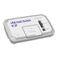
Renesas RL78/G13 User Manual (59 pages)
Emulator
Brand:
Renesas
| Category:
Computer Hardware
| Size: 1 MB
Table of Contents
Table of Contents
4
Overview
7
Overview of E1/E20/E2 Emulator and E2 Emulator Lite
7
Note on Using E20
7
Configuration of E1/E20/E2/E2 Lite Manuals
8
Supported Devices
9
Overview of the Specifications of the External Trigger Input and Output
11
Assignments of the External Trigger Input and Output Pins
11
Specifications of the External Trigger Inputs and Outputs
12
Designing the User System
13
Connecting the E1/E20/E2/E2 Lite to the User System
13
Installing the Connector on the User System
13
Connecting the User System Interface Cable to the 14-Pin Connector
13
Pin Assignments of the Connector on the User System
17
14-Pin Connector Specifications
17
Recommended Circuits between the Connector and the MCU
19
Connection between the 14-Pin Connector and the RL78 Family Mcus in General
19
Connection between the 14-Pin Connector and the RL78 Family Mcus
21
And the 20- and 24-Pin Versions of the RL78/G12)
21
Connection between the 14-Pin Connector and the RL78 Family MCU (Only the RL78/I1C)
22
Notes on Connection
25
RESET# Pin
25
TOOL0 Pin
28
Gnd
29
VDD
29
Internal Circuits of the Emulator
31
Internal Circuits of the E1 (When the RL78 Family Is Connected)
31
Internal Circuits of the E20 (When the RL78 Family Is Connected)
32
Internal Circuits of the E2 (When the RL78 Family Is Connected)
33
Internal Circuits of the E2 Lite (When the RL78 Family Is Connected)
35
Notes on Designing the User System
36
Isolator for the E1
36
Small Connector Conversion Adapter for the E1
36
Notes on Usage
38
Turning the Power On/Off
38
When a Separate Power Supply Is Used for the User System
38
When Power Is Supplied to the User System from the Emulator (E1/E2/E2 Lite Only)
39
Power Supply Function of the E1/E2/E2 Lite
39
MCU Resources to be Occupied
40
Securing an Area for the Debugging Monitor Program
41
Securing a Stack Area for Debugging
42
Setting an On-Chip Debugging Option Byte
43
Setting a Security ID
44
Setting a Serial Programming Security ID
45
Reset
46
Operation after a Reset
46
SP Value after a Reset
46
Flash Memory
46
Flash Memory Programming by Self-Programming
46
Operation for Voltages and Flash Operation Modes Not Permitting Flash Memory Rewriting
47
Advertisement
Renesas RL78/G13 Manual (73 pages)
Brand:
Renesas
| Category:
Microcontrollers
| Size: 0 MB
Table of Contents
Table of Contents
2
Specifications
4
Operation Check Conditions
5
Related Application Note
5
Description of the Hardware
6
Hardware Configuration Example
6
List of Pins to be Used
7
Description of the Software
8
Operation Outline
8
File Configuration
10
List of Option Byte Settings
11
List of Constants
12
List of Variables
13
List of Functions
14
Function Specifications
15
Flowcharts
24
Initialization Function
25
System Function
26
I/O Port Setup
27
CPU Clock Setup
28
TAU0 Setup
29
Real-Time Clock Setup
35
Interval Timer Setup
36
External Interrupt Input Setup
37
Main Processing
38
Starting INTP0 External Interrupt Processing
41
Starting Pulse Interval Measurement
42
Starting Channel 5 of TAU0
43
Stopping Channel 5 of TAU0
44
Getting Count Clock Change Request Flag
45
Getting Pulse Interval Measurement End Flag
46
Judging Pulse Interval Measurement Value
47
Getting Pulse Interval Measurement Value
48
Clearing Pulse Interval Measurement End Flag
49
Changing Count Clock
50
Changing HOCO Clock
51
Starting LED Blink
52
Stopping LED Blink
53
Starting Real-Time Clock
54
Stopping Real-Time Clock
55
Starting Real-Time Clock Fixed-Frequency Interrupt
56
Stopping Real-Time Clock Fixed-Frequency Interrupt
57
Clearing Count Clock Change Request Flag
58
Interval Timer Interrupt
59
Capture End Interrupt for Channel 5 of TAU0
60
INTP0 External Interrupt
61
RTC Fixed-Frequency Interrupt
62
Callback Function for RTC Fixed-Frequency Interrupts
63
Interval Timer Start
64
Stopping Interval Timer
65
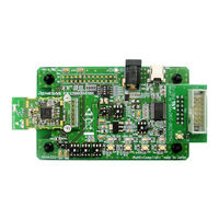
Renesas RL78/G13 User Manual (58 pages)
E1/E20/E2 Emulator, E2 Emulator Lite
Brand:
Renesas
| Category:
Computer Hardware
| Size: 0 MB
Table of Contents
Table of Contents
4
Overview
7
Overview of E1/E20/E2 Emulator and E2 Emulator Lite
7
Note on Using E20
7
Configuration of E1/E20/E2/E2 Lite Manuals
8
Supported Devices
9
Overview of the Specifications of the External Trigger Input and Output
11
Assignments of the External Trigger Input and Output Pins
11
Specifications of the External Trigger Inputs and Outputs
12
Designing the User System
13
Connecting the E1/E20/E2/E2 Lite to the User System
13
Installing the Connector on the User System
13
Connecting the User System Interface Cable to the 14-Pin Connector
13
Pin Assignments of the Connector on the User System
17
14-Pin Connector Specifications
17
Recommended Circuits between the Connector and the MCU
19
Connection between the 14-Pin Connector and the RL78 Family Mcus in General
19
Connection between the 14-Pin Connector and the RL78 Family Mcus (Only the RL78/G11 and the 20- and 24-Pin Versions of the RL78/G12)
21
Connection between the 14-Pin Connector and the RL78 Family MCU (Only the RL78/I1C)
22
Notes on Connection
25
RESET# Pin
25
TOOL0 Pin
28
Gnd
29
VDD
29
Internal Circuits of the Emulator
31
Internal Circuits of the E1 (When the RL78 Family Is Connected)
31
Internal Circuits of the E20 (When the RL78 Family Is Connected)
32
Internal Circuits of the E2 (When the RL78 Family Is Connected)
33
Internal Circuits of the E2 Lite (When the RL78 Family Is Connected)
35
Notes on Designing the User System
36
Isolator for the E1
36
Small Connector Conversion Adapter for the E1
36
Notes on Usage
38
Turning the Power On/Off
38
When a Separate Power Supply Is Used for the User System
38
When Power Is Supplied to the User System from the Emulator (E1/E2/E2 Lite Only)
39
Power Supply Function of the E1/E2/E2 Lite
39
MCU Resources to be Occupied
40
Securing an Area for the Debugging Monitor Program
41
Securing a Stack Area for Debugging
42
Setting an On-Chip Debugging Option Byte
43
Setting a Security ID
44
Setting a Serial Programming Security ID
45
Reset
46
Operation after a Reset
46
SP Value after a Reset
46
Flash Memory
46
Flash Memory Programming by Self-Programming
46
Operation for Voltages and Flash Operation Modes Not Permitting Flash Memory Rewriting
47
Gdidis
47
Renesas RL78/G13 User Manual (55 pages)
Brand:
Renesas
| Category:
Computer Hardware
| Size: 0 MB
Table of Contents
Table of Contents
4
1 Overview
7
Overview of E1/E20/E2 Emulator and E2 Emulator Lite
7
Note on Using E20
7
Configuration of E1/E20/E2/E2 Lite Manuals
8
Supported Devices
9
Overview of the Specifications of the External Trigger Input and Output
11
Assignments of the External Trigger Input and Output Pins
11
Specifications of the External Trigger Inputs and Outputs
12
2 Designing the User System
13
Connecting the E1/E20/E2/E2 Lite to the User System
13
Installing the Connector on the User System
13
Connecting the User System Interface Cable to the 14-Pin Connector
13
Pin Assignments of the Connector on the User System
17
14-Pin Connector Specifications
17
Recommended Circuits between the Connector and the MCU
19
Connection between the 14-Pin Connector and the RL78 Family Mcus in General
19
Connection between the 14-Pin Connector and the RL78 Family Mcus (Only the RL78/G11 and the 20- and 24-Pin Versions of the RL78/G12)
21
Connection between the 14-Pin Connector and the RL78 Family MCU (Only the RL78/I1C)
22
Notes on Connection
25
RESET# Pin
25
TOOL0 Pin
28
Gnd
29
VDD
29
Internal Circuits of the Emulator
31
Internal Circuits of the E1 (When the RL78 Family Is Connected)
31
Internal Circuits of the E20 (When the RL78 Family Is Connected)
32
Internal Circuits of the E2 (When the RL78 Family Is Connected)
33
Internal Circuits of the E2 Lite (When the RL78 Family Is Connected)
35
Notes on Designing the User System
36
Isolator for the E1
36
Small Connector Conversion Adapter for the E1
36
3 Notes on Usage
38
Turning the Power On/Off
38
When a Separate Power Supply Is Used for the User System
38
When Power Is Supplied to the User System from the Emulator (E1/E2/E2 Lite Only)
39
Power Supply Function of the E1/E2/E2 Lite
39
MCU Resources to be Occupied
40
Securing an Area for the Debugging Monitor Program
41
Securing a Stack Area for Debugging
42
Setting an On-Chip Debugging Option Byte
43
Setting a Security ID
44
Reset
45
Operation after a Reset
45
SP Value after a Reset
45
Flash Memory
45
Flash Memory Programming by Self-Programming
45
Operation for Voltages and Flash Operation Modes Not Permitting Flash Memory Rewriting
46
Gdidis
46
RESET# Multiplexed Pin
46
Mcus that Are Used in Debugging
47
Usage in Mass-Production
47
Standalone Operation
47
Final Evaluation of the User Program
47
Debug Functions
48
Stepped Execution
48
Go to Here]
48
Debugging in Standby Mode
48
Pseudo-Real-Time RAM Monitor Function or Pseudo-Dynamic Memory Modification Function
49
Start/Stop Functions
49
Emulation of Flash Memory CRC Accumulator Function
50
Break Function
50
Setting and Deleting Events During User Program Execution
50
Trace Function
50
3.10.10 Battery Backup Function
50
3.10.11 RAM-ECC Function
50
3.10.12 Extended Functions of the E2
51
3.10.13 Points for Caution on Using the RL78/G23
51
Renesas RL78/G13 Operation (54 pages)
Clock Generator (Clock Switching) CC-RL
Brand:
Renesas
| Category:
Microcontrollers
| Size: 0 MB
Table of Contents
Table of Contents
2
1 Specifications
4
2 Operation Check Conditions
6
3 Related Application Note
6
4 Description of the Hardware
7
Hardware Configuration Example
7
List of Pins to be Used
8
5 Software Description
9
Operation Overview
9
File Configuration
10
List of Option Byte Settings
11
List of Constants
12
List of Variables
13
List of Functions
13
Function Specifications
14
Flowcharts
21
Initialization Function
22
System Function
23
I/O Port Setup
24
CPU Clock Setup
25
Timer Array Unit 0 (TAU0) Setup
29
Setting up 12-Bit Interval Timer
30
Setting up External Interrupt Input
31
Main Processing
32
Setting to Start INTP0 External Interrupt Processing
33
Setting to Start Operation of Channel 0 of TAU0
34
Switching Clock
35
Switching from HOCO Clock to X1 Oscillation Clock
36
Switching from X1 Oscillation Clock to XT1 Oscillation Clock
37
Switching from XT1 Oscillation Clock to HOCO Clock
38
Getting Clock Status
39
Getting X1 Oscillation Clock Status
40
Getting XT1 Oscillation Clock Status
41
Getting HOCO Clock Status
42
Stopping Clock
43
Getting Parameters of Channel 0 of TAU0
44
Restarting Channel 0 of TAU0
45
Changing Interval of Channel 0 of TAU0
46
Setting to Stop Channel 0 of TAU0
47
Processing of Interval Timer Interrupt of Channel 0 of TAU0
48
Processing of INTP0 External Interrupt
49
Waiting in Units of 1 Ms
50
6 Sample Code
51
Renesas RL78/G13 User Manual (37 pages)
Brand:
Renesas
| Category:
Computer Hardware
| Size: 1 MB
Table of Contents
How to Use this Manual
4
Table of Contents
6
Overview
7
Purpose
7
Features
7
Power Supply
8
Requirements
8
Power-Up Behaviour
8
Board Layout
9
Component Layout
9
Board Dimensions
10
Component Placement
11
Connectivity
12
Internal RSK Connections
12
Debugger Connections
13
User Circuitry
14
Reset Circuit
14
Clock Circuit
14
Switches
14
Leds
14
Potentiometer
15
Debug LCD Module
15
RS232 Serial Port
15
Local-Interconnect Network (LIN)
15
Configuration
17
Modifying the RSK
17
MCU Configuration
17
ADC Configuration
17
RS232 Serial Port Configuration
18
LIN Configuration
19
IRQ & General I/O Pin Configuration
20
Power Supply Configuration
21
Clock Configuration
23
Headers
24
Application Headers
24
Microcontroller Ring Headers
26
Code Development
30
Overview
30
Compiler Restrictions
30
Mode Support
30
Debugging Support
30
Address Space
31
Additional Information
32
Revision History
33
Renesas RL78/G13 Application Note (40 pages)
Handshake-based SPI Master Transmission/Reception
Brand:
Renesas
| Category:
Computer Hardware
| Size: 0 MB
Table of Contents
Table of Contents
2
Specifications
4
Outline of CSI Communication
4
Outline of Communication
5
Communication Format
7
Handshake
7
Specification Details
8
Operation Confirmation Conditions
11
Related Application Notes
11
Hardware Descriptions
12
Example of Hardware Configuration
12
List of Pins to be Used
13
Description of the Software
14
List of Option Byte Settings
14
List of Constants
14
List of Variables
15
List of Functions
16
Function Specifications
16
Flowcharts
22
Initialization Process
22
Reset Source Reading
22
CPU Clock Configuration
23
Port Configuration
23
SAU Configuration
24
CSI00 Configuration
25
TAU0 Configuration
26
Flowchart of Main Processing
27
User Main Initialization
28
TAU0 Channel 3 Upper 8 Bits Start Operation
29
CSI00 Start Operation
29
CSI00 Transmit/Receive Processing
30
INICSI00 Interrupt Processing
31
Flowchart of CSI Status Check
32
Flowchart of CSI Transmission/Reception
33
Flowchart of CSI Transmission
34
Flowchart of CSI Reception
35
Flowchart of Wait for Slave Response
36
Sample Code
37
Reference Documents
37
Renesas RL78/G13 User Manual (26 pages)
Renesas Starter Kit Software
Brand:
Renesas
| Category:
Controller
| Size: 0 MB
Table of Contents
Table of Contents
6
1 Overview
8
Purpose
8
2 Introduction
9
3 RSK Sample Code Concept
10
Sample Code Structure
10
List of Sample Code
11
4 Tutorial Sample
12
Tutorial
12
Description
12
Operation
12
Application
13
Description
13
5 Peripheral Samples
14
Adc_Oneshot
14
Description
14
Operation
14
Adc_Repeat
14
Operation
15
Lin
15
Description
15
Async_Serial
16
Description
16
Operation
16
Sync_Serial
16
Lvd
17
Description
17
Operation
17
Iic_Master
17
Iic_Slave
18
Description
18
IIC Slave Commands
18
Operation
19
Timer
19
Description
19
Dmac
20
Description
20
Operation
20
Wdt
20
Operation
21
Rtc
21
Description
21
Renesas RL78/G13 User Manual (30 pages)
Brand:
Renesas
| Category:
Media Converter
| Size: 1 MB
Table of Contents
Table of Contents
6
Overview
7
Purpose
7
Features
7
Introduction
8
Introduction to Applilet
9
What Is Applilet
9
Features
9
Applilet Application Models
9
Project Creation
10
Tutorial Project Workspace
12
Project Workspace
13
Introduction
13
Starting IAR Embedded Workbench
13
Build Configuration
16
Building the Tutorial Program
17
Building Code
17
Connecting the Debugger
18
Connecting to the Target with the E1 Debugger
18
Running the Tutorial
20
Downloading the Program Code
20
Reviewing the Tutorial Program
21
Program Initialisation
21
Main Functions
22
Additional Information
25
Renesas RL78/G13 Hardware Manual (13 pages)
PMOD Module
Brand:
Renesas
| Category:
Control Unit
| Size: 0 MB
Table of Contents
Table of Contents
2
1 Overview
3
Specification Outline
3
2 RL78/G1D-SK PMOD Module Interface
4
3 RL78/G1D-SK Bluetooth Module Pin Configuration
5
4 RL78/G1D-SK PMOD Module Design Bill of Material
6
5 Circuit Diagrams
7
Appendix A - References
7
Appendix B - Conformity Assessment
8
Advertisement
Related Products
Renesas RL78/G10
Renesas RL78/G1A
Renesas rl78/g1g
Renesas RL78/G1H
Renesas RL78/G1P
Renesas RL78/G1M
Renesas RL78/G1N
Renesas RL78/G23-128p
Renesas RL78/G15
Renesas RL78 Series
Renesas Categories
Computer Hardware
Motherboard
Microcontrollers
Adapter
Switch
More Renesas Manuals
Login
Sign In
OR
Sign in with Facebook
Sign in with Google
Upload manual
Upload from disk
Upload from URL