Table of Contents
Advertisement
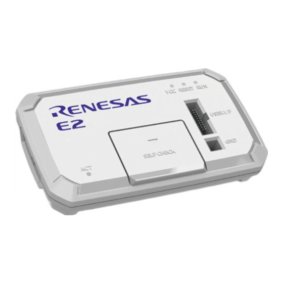
E1/E20/E2 Emulator, E2 Emulator Lite
Supported Devices:
RL78 Family
RL78/D1A, RL78/F12, RL78/F13, RL78/F14, RL78/F15, RL78/F1A,
RL78/G11, RL78/G12, RL78/G13, RL78/G14, RL78/G1A, L78/G1C,
RL78/G1D, RL78/G1E, RL78/G1F, RL78/G1G, RL78/G1H,
RL78/G1P, RL78/G13A, RL78/G23,
RL78/I1A, RL78/I1B, RL78/I1C, RL78/I1D, RL78/I1E,
RL78/L12, RL78/L13, RL78/L1A, RL78/L1C,
RL78/FGIC
All information contained in these materials, including products and product specifications,
represents information on the product at the time of publication and is subject to change by
Renesas Electronics Corporation without notice. Please review the latest information published
by Renesas Electronics Corporation through various means, including the Renesas Electronics
Corporation website (http://www.renesas.com).
Additional Document for User's Manual
(Notes on Connection of RL78)
Rev.8.00 Mar 2021
Advertisement
Table of Contents

Related Manuals for Renesas RL78 Series


Summary of Contents for Renesas RL78 Series
- Page 1 All information contained in these materials, including products and product specifications, represents information on the product at the time of publication and is subject to change by Renesas Electronics Corporation without notice. Please review the latest information published by Renesas Electronics Corporation through various means, including the Renesas Electronics Corporation website (http://www.renesas.com).
- Page 2 Renesas Electronics disclaims any and all liability for any damages or losses incurred by you or any third parties arising from the use of any Renesas Electronics product that is inconsistent with any Renesas Electronics data sheet, user’s manual or other Renesas Electronics document.
- Page 3 Unit Products The following usage notes are applicable to all Microprocessing unit and Microcontroller unit products from Renesas. For detailed usage notes on the products covered by this document, refer to the relevant sections of the document as well as any technical updates that have been issued for the products.
-
Page 4: Table Of Contents
E1/E20/E2/E2 Lite Additional Document Contents Contents 1. Overview .......................... 7 Overview of E1/E20/E2 Emulator and E2 emulator Lite ................7 Note on Using E20 ........................... 7 Configuration of E1/E20/E2/E2 Lite Manuals ..................8 Supported Devices ........................... 9 Overview of the Specifications of the External Trigger Input and Output ..........11 1.5.1 Assignments of the External Trigger Input and Output Pins ............ - Page 5 E1/E20/E2/E2 Lite Additional Document Contents MCUs that are Used in Debugging ......................47 3.8.1 Usage in Mass-Production ......................47 3.8.2 Standalone Operation ........................47 Final Evaluation of the User Program ....................47 3.10 Debug Functions ............................ 48 3.10.1 Stepped Execution ........................48 3.10.2 [Go to Here] ..........................
- Page 6 User program This means the program to be debugged. Programming Software In this document, this indicates Renesas Flash Programmer that can be used with the E1, E20, E2, or E2 Lite. "#" at the end of a pin name (signal name) "#"...
-
Page 7: Overview
In this document, we describe ‘E2 Emulator’ as ‘E2’, ‘E1 Emulator’ as ‘E1’, ‘E20 Emulator’ as ‘E20’ and ‘E2 emulator Lite’ as ‘E2 Lite’. The E1, E20, E2, and E2 Lite are on-chip debugging emulators for Renesas' mainstream MCUs. The E1 and E2 Lite are highly affordable development tools providing basic debugging functions. The E20 is a development tool allowing sophisticated debugging through enhanced functions such as tracing and RAM monitoring as well as the basic debugging functions of the E1 and E2 Lite. -
Page 8: Configuration Of E1/E20/E2/E2 Lite Manuals
E1/E20/E2/E2 Lite Additional Document 1. Overview Configuration of E1/E20/E2/E2 Lite Manuals The E1, E20, E2, and E2 Lite manuals consist of the following. E2 Emulator User’s Manual • • E1/E20 Emulator User's Manual E2 Emulator Lite User’s Manual • E1/E20/E2 Emulator, E2 Emulator Lite Additional Document for User’s Manual •... -
Page 9: Supported Devices
E1/E20/E2/E2 Lite Additional Document 1. Overview Supported Devices Table 1-1 Supported Device List Item Description Target MCUs *2 RL78 Family (RL78-S2 Core) *1 RL78/D1x: RL78/D1A RL78/F1x: RL78/F12 RL78/G1x: RL78/G12, RL78/G13, RL78/G1A, RL78/G1C, RL78/G1D, RL78/G1E, RL78/G1P, RL78/G13A RL78/I1x: RL78/I1A RL78/L1x: RL78/L12, RL78/L13 RL78 Family (RL78-S3 Core) *1 RL78/F1x: RL78/F13, RL78/F14, RL78/F15, RL78/F1A... - Page 10 E1/E20/E2/E2 Lite Additional Document 1. Overview Table 1-2 Debugging Function List Item Type of the RL78 Core Description RL78-S2 RL78-S3 Memory reference or change during program execution Pseudo-real-time RAM monitor Supported Supported CPU is used when monitoring (RRM) Dynamic Memory Modification Supported Supported CPU is used when changing...
-
Page 11: Overview Of The Specifications Of The External Trigger Input And Output
E1/E20/E2/E2 Lite Additional Document 1. Overview Overview of the Specifications of the External Trigger Input and Output This section describes the specifications of the external trigger input and output, which is one of extended functions of the E2. 1.5.1 Assignments of the External Trigger Input and Output Pins The following figure and table show the assignments of the external trigger input and output pins for the E2 expansion interface. -
Page 12: Specifications Of The External Trigger Inputs And Outputs
E1/E20/E2/E2 Lite Additional Document 1. Overview Table 1-3 Assignments of the External Trigger Input and Output Pins for the E2 Expansion Interface Pin No. Input/Output Description ⎯ Pin Nos. 1 to 8 are not used. ⎯ These pins must be left open-circuit. ⎯... -
Page 13: Designing The User System
E1/E20/E2/E2 Lite Additional Document 2. Designing the User System 2. Designing the User System Connecting the E1/E20/E2/E2 Lite to the User System To connect the E1/E20/E2/E2 Lite to the user system, a connector for the user system interface cable must be mounted on the user system. - Page 14 E1/E20/E2/E2 Lite Additional Document 2. Designing the User System 38-pin user-system interface cable 9.4 mm 26.2 mm 38-pin to 14-pin conversion adapter 14-pin connector 7614-6002 or 38-pin to 14-pin conversion adapter (top view) 2514-6002 R0E000200CKA00 10 mm (include in the E20 package) User system Figure 2-2 Connecting the User System Interface Cable to the 14-Pin Connector of the E20 Emulator 20-pin (1.27-mm pin spacing) user-system...
- Page 15 E1/E20/E2/E2 Lite Additional Document 2. Designing the User System CAUTION Limit to the height on connector periphery: For a case where the R0E000200CKA00 is used for connecting the E20 to a 14-pin connector, do not mount other components with a height of 10 mm or more within 5 mm of the connector on the user system.
- Page 16 E1/E20/E2/E2 Lite Additional Document 2. Designing the User System CAUTION Limit to the height on connector periphery: If the 20-pin (1.27-mm pin spacing) to 14-pin (2.54-mm pin spacing) connector conversion adapter is in use and the E2 is to be connected to the 14-pin connector, do not mount components with a height of 13 mm or more on the user system within a rectangle 2 mm from the edges of the connector.
-
Page 17: Pin Assignments Of The Connector On The User System
E1/E20/E2/E2 Lite Additional Document 2. Designing the User System Pin Assignments of the Connector on the User System 2.3.1 14-Pin Connector Specifications Figure 2-4 shows the specifications of the 14-pin connector. Table 2-2 on the following pages shows the pin assignments of the 14-pin connector. Pin 1 mark Connector 25.0... - Page 18 - - For details on the programming software, refer to the following. https://www.renesas.com/RFP “Input” refers to input from the emulator to the user system and “output” refers to output from the user system to the emulator. Securely connect pins 2, 12, and 14 of the connector to GND of the user system. These pins are used for electrical grounding as well as for monitoring of connection with the user system by the E1/E20/E2/E2 Lite.
-
Page 19: Recommended Circuits Between The Connector And The Mcu
E1/E20/E2/E2 Lite Additional Document 2. Designing the User System Recommended Circuits between the Connector and the MCU This section shows recommended circuits for connection between the connector and the MCU when the E1/E20/E2/E2 Lite is in use. For processing of signals, refer to section 2.5, Notes on Connection. 2.4.1 Connection between the 14-Pin Connector and the RL78 Family MCUs in General Figure 2-5 shows a recommended circuit for connection between the 14-pin connector and the RL78 family... - Page 20 E1/E20/E2/E2 Lite Additional Document 2. Designing the User System Notes: The circuits and resistance values listed are recommended but not guaranteed. Determine the circuit design and resistance values by taking into account the specifications of the target device and noise. For flash programming for mass production, perform sufficient evaluation about whether the specifications of the target device are satisfied.
-
Page 21: Connection Between The 14-Pin Connector And The Rl78 Family Mcus (Only The Rl78/G11 And The 20- And 24-Pin Versions Of The Rl78/G12)
E1/E20/E2/E2 Lite Additional Document 2. Designing the User System 2.4.2 Connection between the 14-Pin Connector and the RL78 Family MCUs (Only the RL78/G11 and the 20- and 24-Pin Versions of the RL78/G12) Figure 2-6 shows a recommended circuit for connection between the 14-pin connector and the RL78 family MCUs (only the RL78/G11 and the 20- and 24-pin versions of the RL78/G12). -
Page 22: Connection Between The 14-Pin Connector And The Rl78 Family Mcu (Only The Rl78/I1C)
E1/E20/E2/E2 Lite Additional Document 2. Designing the User System 2.4.3 Connection between the 14-Pin Connector and the RL78 Family MCU (Only the RL78/I1C) The following shows a recommended circuit for connection between the 14-pin connector and the RL78 family MCU (only the RL78/I1C). Figure 2-7 shows the case when the battery backup function is in use. - Page 23 E1/E20/E2/E2 Lite Additional Document 2. Designing the User System Notes: The circuits and resistance values listed are recommended but not guaranteed. Determine the circuit design and resistance values by taking into account the specifications of the target device and noise. For flash programming for mass production, perform sufficient evaluation about whether the specifications of the target device are satisfied.
- Page 24 E1/E20/E2/E2 Lite Additional Document 2. Designing the User System 14-pin 2.54-mm pitch Note 1 Note 2 connector RSTPU Note 3 Note 4 1 kW Note 3 RESET_IN Reset circuit Note 3 470 to 510 W 10,13 RESET# RESET_OUT Note 3 Note 6 Note 7 Note 7 EVDD...
-
Page 25: Notes On Connection
E1/E20/E2/E2 Lite Additional Document 2. Designing the User System Notes on Connection Wiring patterns between the connector and the MCU must be as short as possible (within 50 mm is recommended). Do not connect the signal lines between the connector and MCU to other signal lines on the board. - Page 26 E1/E20/E2/E2 Lite Additional Document 2. Designing the User System <Connection Example of RESET for RL78 Family MCUs in General> (Recommended Circuit) 1 kW 14-pin Note 2 2.54-mm pitch Reset circuit connector Note 1 RESET_IN 10 kW Note 2 10,13 RESET_OUT RESET# Note 1: The emulator operates for flash programming by the programming software whether this pin is connected or not.
- Page 27 E1/E20/E2/E2 Lite Additional Document 2. Designing the User System <Connection Example of RESET when the Target MCU is an RL78/I1C with the Battery Backup Function in Use> (Recommended Circuit) 14-pin 2.54-mm pitch connector Note 2 RSTPU 1 kW Note 1 Reset circuit RESET_IN 470 to 510 W...
-
Page 28: Tool0 Pin
E1/E20/E2/E2 Lite Additional Document 2. Designing the User System 2.5.2 TOOL0 Pin The E1/E20/E2/E2 Lite uses the TOOL0 pin. Any functions that are multiplexed on this pin are not available. Pull up the signals of the TOOL0 pin at 1 kΩ and do not arrange these signal lines in parallel with or across other high-speed signal lines. -
Page 29: Gnd
When writing a program that requires reliability, do not use the power supply function of the E1/E2/E2 Lite. Use a stable, separate power supply for the user system. When writing a program for mass production processes, use the Renesas Flash Programmer. For details on the programming software, refer to: https://www.renesas.com/RFP... - Page 30 E1/E20/E2/E2 Lite Additional Document 2. Designing the User System WARNING Warning for Turning the Power On/Off: When supplying power, ensure that there are no shorts between VDD and GND. Only connect the E1/E20/E2/E2 Lite after confirming that there are no mismatches of alignment on the user system port connector.
-
Page 31: Internal Circuits Of The Emulator
E1/E20/E2/E2 Lite Additional Document 2. Designing the User System Internal Circuits of the Emulator 2.6.1 Internal Circuits of the E1 (when the RL78 Family is Connected) Figure 2-16 shows the internal circuits of the E1 with the RL78 family connected. User-side connector 100 kW ×... -
Page 32: Internal Circuits Of The E20 (When The Rl78 Family Is Connected)
E1/E20/E2/E2 Lite Additional Document 2. Designing the User System 2.6.2 Internal Circuits of the E20 (when the RL78 Family is Connected) Figure 2-17 shows the internal circuits of the E20 with the RL78 family connected. User-side 100 kW × 3 connector 3.3 V 22 W... -
Page 33: Internal Circuits Of The E2 (When The Rl78 Family Is Connected)
E1/E20/E2/E2 Lite Additional Document 2. Designing the User System 2.6.3 Internal Circuits of the E2 (when the RL78 Family is Connected) Figure 2-18 and Figure 2-19 respectively show the internal circuits of product revisions C and D of the E2 with the RL78 family connected. - Page 34 E1/E20/E2/E2 Lite Additional Document 2. Designing the User System User-side connector 1 MW × 2 Power-supply circuit (only for use in the mode to supply power to the user system) 100 kW 3.3 V 47 W 74LVC1T45 RSTPU 3 MW 74LVC8T245 EMVDD EMVDD...
-
Page 35: Internal Circuits Of The E2 Lite (When The Rl78 Family Is Connected)
E1/E20/E2/E2 Lite Additional Document 2. Designing the User System 2.6.4 Internal Circuits of the E2 Lite (when the RL78 Family is Connected) Figure 2-20 shows the internal circuits of the E2 Lite with the RL78 family connected. User-side 100 kW × 5 connector Power-supply circuit (only for use in the mode to... -
Page 36: Notes On Designing The User System
Small Connector Conversion Adapter for the E1 A small connector conversion adapter for the E1 (R0E000010CKZ11) is separately available from Renesas for user system boards which are too small to mount the 14-pin connector that is the standard connector for the E1, E2, and E2 Lite. - Page 37 - - For details on the programming software, refer to the following. https://www.renesas.com/RFP “Input” refers to input from the emulator to the user system and “output” refers to output from the user system to the emulator. Securely connect pins 1, 6, and 14 of the connector to GND of the user system. These pins are used for electrical grounding as well as for monitoring of connection with the user system by the E1/E20/E2 Lite.
-
Page 38: Notes On Usage
E1/E20/E2/E2 Lite Additional Document 3. Notes on Usage 3. Notes on Usage Turning the Power On/Off Turn the power of the E1/E20/E2/E2 Lite and the user system following the procedure below. 3.1.1 When a Separate Power Supply is Used for the User System <When using the emulator>... -
Page 39: When Power Is Supplied To The User System From The Emulator (E1/E2/E2 Lite Only)
E1/E20/E2/E2 Lite Additional Document 3. Notes on Usage 3.1.2 When Power is Supplied to the User System from the Emulator (E1/E2/E2 Lite Only) <When using the emulator> (1) Connect the user system. Connect the emulator and the user system with a user-system interface cable. When the external trigger input/output function is to be used with the E2, connect the pins to be used. -
Page 40: Mcu Resources To Be Occupied
E1/E20/E2/E2 Lite Additional Document 3. Notes on Usage MCU Resources to be Occupied Figure 3-1 shows the areas which are occupied by the E1/E20/E2/E2 Lite for debugging. These areas (shaded sections) are used for debugging. These areas should not be changed to save the user program or data. -
Page 41: Securing An Area For The Debugging Monitor Program
E1/E20/E2/E2 Lite Additional Document 3. Notes on Usage The reset vector area is used by the program for the E1/E20/E2/E2 Lite when performing debugging with the E1/E20/E2/E2 Lite. If the contents of the reset vector area are changed, control by the E1/E20/E2/E2 Lite is no longer possible. -
Page 42: Securing A Stack Area For Debugging
E1/E20/E2/E2 Lite Additional Document 3. Notes on Usage 3.3.2 Securing a Stack Area for Debugging The debugger requires 4 bytes as a stack area for debugging except if start/stop functions (only supported by the E2/E2 Lite) are in use, in which case the size of the stack area for debugging is up to 8 bytes. Since this area is allocated immediately below the main stack area, the address of this area varies with increases and decreases in the stack size. -
Page 43: Setting An On-Chip Debugging Option Byte
E1/E20/E2/E2 Lite Additional Document 3. Notes on Usage 3.3.3 Setting an On-Chip Debugging Option Byte This is the area for the security setting to prevent the flash memory from being read by an unauthorized person. For settable values, refer to the user's manual for each MCU. When an on-chip debugging emulator is to be connected, be sure to set a security ID. -
Page 44: Setting A Security Id
E1/E20/E2/E2 Lite Additional Document 3. Notes on Usage 3.3.4 Setting a Security ID This setting is required to prevent the memory from being read by an unauthorized person. Embed a security ID at addresses 0xC4 to 0xCD in the internal flash memory. The debugger starts only when the security ID that is set during debugger startup and the security ID set at addresses 0xC4 to 0xCD match. -
Page 45: Reset
E1/E20/E2/E2 Lite Additional Document 3. Notes on Usage Reset 3.4.1 Operation after a Reset After an external pin reset or internal reset, the monitor program performs debug initialization processing. Consequently, the time from reset occurrence until user program execution differs from that in the actual device operation. -
Page 46: Operation For Voltages And Flash Operation Modes Not Permitting Flash Memory Rewriting
E1/E20/E2/E2 Lite Additional Document 3. Notes on Usage 3.5.2 Operation for Voltages and Flash Operation Modes Not Permitting Flash Memory Rewriting When a voltage with which rewriting or erasure of flash memory cannot be performed has been selected or flash programming has been disabled with the debugger's property, the following debugger operations that accompany flash memory rewriting will cause an error in the debugger and the operations will be invalidated. -
Page 47: Mcus That Are Used In Debugging
Final Evaluation of the User Program Before entering the mass-production phase, be sure to perform a final evaluation of the program which has been written to the flash ROM by the Renesas Flash Programmer programming software or a flash programmer, without the emulator connected. -
Page 48: Debug Functions
E1/E20/E2/E2 Lite Additional Document 3. Notes on Usage 3.10 Debug Functions 3.10.1 Stepped Execution (1) Cautions on using step-in (stepped execution) The value of some SFRs (special function registers) might remain unchanged while stepping into code. If the values of the SFRs do not change while stepping into code, operate the microcontroller by continuously executing the instructions instead of executing them in steps. -
Page 49: Pseudo-Real-Time Ram Monitor Function Or Pseudo-Dynamic Memory Modification Function
E1/E20/E2/E2 Lite Additional Document 3. Notes on Usage 3.10.4 Pseudo-Real-Time RAM Monitor Function or Pseudo-Dynamic Memory Modification Function Note the following points when using the pseudo-real-time RAM monitor (RRM) function or the pseudo- Dynamic Memory Modification (DMM) function. • Standby mode (HALT or STOP) may be cancelled during monitoring. •... -
Page 50: Emulation Of Flash Memory Crc Accumulator Function
E1/E20/E2/E2 Lite Additional Document 3. Notes on Usage 3.10.6 Emulation of Flash Memory CRC Accumulator Function (1) High-speed CRC (code flash: all area) The operation result of CRC is different from actual result. Because monitor program is arranged and reset vector is rewritten by on-chip debugging. Please check the operation of high-speed CRC by using IECUBE or using device without E1/E20/E2/E2 Lite. -
Page 51: 3.10.12 Extended Functions Of The E2
E1/E20/E2/E2 Lite Additional Document 3. Notes on Usage 3.10.12 Extended Functions of the E2 3.10.12.1 Solution for the Tuning of Current Consumption For notes on the solution for the tuning of current consumption, refer to the application note. 3.10.12.2 External Trigger Input and Output •... - Page 52 E1/E20/E2/E2 Lite Additional Document 3. Notes on Usage 3.10.13.2 Operation with 1.8-V and Lower Voltages When you are using the RL78/G23 with 1.8-V or a lower voltage, specify [Yes] for [Use wide voltage mode] (for CS+) and [Use Wide Voltage Mode] (for the e studio) in the [Connect Settings] tabbed page of the debugger.
- Page 53 E1/E20/E2 Emulator, E2 Emulator Lite Revision History Additional Document for User's Manual (Notes on Connection of RL78) Rev. Date Description Page Summary 4.01 Mar.16.16 Information on the RL78/F15, RL78/G1H, and RL78/I1E groups was added. Note (3) was added to section 3.5.1. 5.00 Mar.16.16 Information on the RL78/I1C and RL78/L1A groups was added.
- Page 54 E1/E20/E2 Emulator, E2 Emulator Lite Additional Document for User's Manual (Notes on Connection of RL78) Publication Date: Rev.8.00 Mar.16.21 Published by: Renesas Electronics Corporation...
- Page 55 E1/E20/E2 Emulator, E2 Emulator Lite Additional Document for User’s Manual (Notes on Connection of RL78) R20UT1994EJ0800...
Need help?
Do you have a question about the RL78 Series and is the answer not in the manual?
Questions and answers