Xilinx ZCU106 User Manual
Hide thumbs
Also See for ZCU106:
- Quick start manuals (4 pages) ,
- User manual (86 pages) ,
- Manual (34 pages)
Table of Contents
Advertisement
Quick Links
Advertisement
Table of Contents

Related Manuals for Xilinx ZCU106


Summary of Contents for Xilinx ZCU106
- Page 1 ZCU106 Evaluation Board User Guide UG1244 (v1.0) March 28, 2018...
-
Page 2: Revision History
Revision History The following table shows the revision history for this document. Date Version Revision 03/28/2018 Initial Xilinx release. ZCU106 Board User Guide Send Feedback UG1244 (v1.0) March 28, 2018 www.xilinx.com... -
Page 3: Table Of Contents
Installing the ZCU106 Board in a PC Chassis........ - Page 4 ZCU106 Board Constraints File Listing ........
- Page 5 Xilinx Resources ........
-
Page 6: Chapter 1: Introduction
Chapter 1 Introduction Overview The ZCU106 is a general purpose evaluation board for rapid-prototyping based on the ® ™ ZU7EV silicon part and package in the 16 nm FinFET Zynq UltraScale+ MPSoC. The ® ™ ZU7EV device integrates a quad core ARM... -
Page 7: Block Diagram
Chapter 1: Introduction Block Diagram The ZCU106 board block diagram is shown in Figure 1-1. X-Ref Target - Figure 1-1 Bank 503 X19000-032318 Figure 1-1: ZCU106 Evaluation Board Block Diagram ZCU106 Board User Guide Send Feedback UG1244 (v1.0) March 28, 2018... -
Page 8: Board Features
Chapter 1: Introduction Board Features The ZCU106 evaluation board features are listed here. Detailed information for each feature is provided in Component Descriptions in Chapter • XCZU7EV-2, FFVC1156 package • PL V for range in data sheet CCINT • Form factor for PCIe® Gen[1-3]x4 endpoint (PL GTH transceiver), Micro-ATX chassis footprint •... - Page 9 Operational status LEDs (power status, INIT, DONE, PG, JTAG status, DDR power good) • Power management The ZCU106 provides designers a rapid prototyping platform using the XCZU7EV-2FFVC1156 device. The ZU7EV contains many PS hard block peripherals exposed through the multi-use I/O (MIO) interface and several FPGA programmable logic (PL), high-density (HD), and high-performance (HP) banks.
-
Page 10: Board Specifications
Length: 9.5 inch (24.13 cm) Thickness: 0.062 inch ±0.005 inch (0.157 cm ±0.0127 cm) A 3D model of this board is not available. Note: The ZCU106 board height exceeds the standard 4.376 inch (11.15 cm) height of a PCI IMPORTANT: ® Express card. -
Page 11: Environmental
Chapter 1: Introduction Environmental Temperature Operating: 0°C to +45°C Storage: -25°C to +60°C Humidity 10% to 90% non-condensing Operating Voltage +12 V ZCU106 Board User Guide Send Feedback UG1244 (v1.0) March 28, 2018 www.xilinx.com... -
Page 12: Chapter 2: Board Setup And Configuration
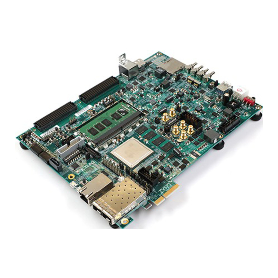
Always refer to the schematic, layout, and XDC files of the specific ZCU106 version of interest for such details. The ZCU106 board can be damaged by electrostatic discharge (ESD). Follow standard ESD CAUTION! prevention measures when handling the board. - Page 13 Round callout references a component Square callout references a component on the front side of the board on the back side of the board X19001-022218 Figure 2-1: ZCU106 Evaluation Board Components ZCU106 Board User Guide Send Feedback UG1244 (v1.0) March 28, 2018 www.xilinx.com...
- Page 14 Chapter 2: Board Setup and Configuration Table 2-1: ZCU106 Board Component Locations Callout Schematic Ref. Des. Feature ([B] = bottom of board) Notes Number Page Zynq UltraScale+ XCZU7EV MPSoC, XCZU7EV-2FFVC1156 Transceivers, PS GTR Transceivers LOTES ADDR0067-P001A/KINGSTON PS-Side: DDR4 SODIMM Socket...
- Page 15 Chapter 2: Board Setup and Configuration Table 2-1: ZCU106 Board Component Locations (Cont’d) Callout Schematic Ref. Des. Feature ([B] = bottom of board) Notes Number Page SW14- E-switch TL3301EP100QG placed in User I/O pushbuttons SW18 N,S,W,E,C pattern SW20 User I/O...
-
Page 16: Default Jumper And Switch Settings
Chapter 2: Board Setup and Configuration Default Jumper and Switch Settings Figure 2-2 shows the ZCU106 board jumper header and DIP switch locations. Each numbered component shown in the figure is keyed to Table 2-2 Table 2-3 (for default switch settings). Both tables reference the respective schematic (0381770) page numbers. -
Page 17: Jumpers
• 1-2: VSUPPLY = VCCOPS3 (1.8V) VCCO_PSDDR_504 select • 1-2: Switched DDR4 VDDQ • 3-4: Direct DDR4 VDDQ DDR4 reset suspend enable J159 • 1-2: Suspend disabled (gate bypass) • 2-3: Suspend enabled ZCU106 Board User Guide Send Feedback UG1244 (v1.0) March 28, 2018 www.xilinx.com... - Page 18 • 1-2: Connector ID • 2-3: VDD33 ID Shield GND select J112 • 1-2: Capacitor • 2-3: GND Device or host select • 1-2: Host/OTG Open • Open: Device ZCU106 Board User Guide Send Feedback UG1244 (v1.0) March 28, 2018 www.xilinx.com...
-
Page 19: Switches
3: SW2 toward the label ON is a 0. 1 through 5 are tied to MSP430 U41 GPIO[1:5]. 4: SW3 5: SW4 SW13 GPIO All Off Main power switch ZCU106 Board User Guide Send Feedback UG1244 (v1.0) March 28, 2018 www.xilinx.com... -
Page 20: Installing The Zcu106 Board In A Pc Chassis
Figure 2-3. a. Plug the 6-pin 2 x 3 Molex connector on the adapter cable into J52 on the ZCU106 board. b. Plug the 4-pin 1 x 4 peripheral power connector from the ATX power supply into the 4-pin adapter cable connector. -
Page 21: Mpsoc Device Configuration
J52. The ATX 6-pin connector has a different pin out than J52. Connecting an ATX 6-pin connector into J52 damages the ZCU106 evaluation board and voids the board warranty. 8. Slide the ZCU106 board power switch SW1 to the ON position. The PC can now be powered on. -
Page 22: Quad Spi
3. Either power-cycle or press the power-on reset (POR) pushbutton. SW6 is callout 46 in Figure 2-1. See the Zynq UltraScale+ MPSoC Technical Reference Manual (UG1085) [Ref 2] for more information about Zynq UltraScale+ MPSoC configuration options. ZCU106 Board User Guide Send Feedback UG1244 (v1.0) March 28, 2018 www.xilinx.com... -
Page 23: Chapter 3: Board Component Descriptions
Cortex -A53 64-bit quad-core processor and Cortex-R5 dual-core real-time processor. Production ZCU106 evaluation boards will ship with -2 speed grade devices. Support of multiple speed grades requires voltage adjustments. The V supplies are user adjustable via the PMBus with the voltage ranges listed in... - Page 24 0.876 For -1LI and -2LE (V = 0.72V) devices: CCINT 0.698 0.720 0.742 CCINT PL internal supply voltage. For -3E devices: PL internal supply voltage. 0.873 0.900 0.927 ZCU106 Board User Guide Send Feedback UG1244 (v1.0) March 28, 2018 www.xilinx.com...
- Page 25 AES-GCM Processor System PCIe DDRC (DDR4/3/3L, LPDDR3/4) 128 KB RAM To ACP Gen4 32-bit/64-bit Battery Low Power Full Power Power 64-bit 128-bit X16387-050517 Figure 3-1: Top-Level Block Diagram ZCU106 Board User Guide Send Feedback UG1244 (v1.0) March 28, 2018 www.xilinx.com...
- Page 26 For additional information on Zynq UltraScale+ MPSoC devices, see the Zynq UltraScale+ MPSoC Data Sheet: Overview (DS891) [Ref 1]. See the Zynq UltraScale+ MPSoC Technical Reference Manual (UG1085) [Ref 2] for more information about Zynq UltraScale+ MPSoC configuration options. ZCU106 Board User Guide Send Feedback UG1244 (v1.0) March 28, 2018 www.xilinx.com...
- Page 27 Chapter 3: Board Component Descriptions Encryption Key Battery Backup Circuit The XCZU7EV MPSoC U1 implements bit stream encryption key technology. The ZCU106 board provides the encryption key backup battery circuit shown in Figure 3-2. X-Ref Target - Figure 3-2 To MPSoC U1 Pin Y23...
-
Page 28: Ps-Side: Ddr4 Sodimm Socket
Chapter 3: Board Component Descriptions I/O Voltage Rails The XCZU7EV MPSoC PL I/O bank voltages on the ZCU106 board are listed in Figure 3-2. Table 3-2: I/O Voltage Rails XCZU7EV Power Net Name Voltage Connected To PL Bank 28 1.8V... - Page 29 Chapter 3: Board Component Descriptions The ZCU106 supports full power-off suspend mode where only the system controller and the PS-side DDR4 SODIMM memory are powered. The DDR4 memory is kept in a self-refresh state and has its reset input controlled by the system controller such that the memory is not reset when waking-up from suspend mode.
- Page 30 DDR4_SODIMM_DQ35 DQ35 AC31 DDR4_SODIMM_DQ36 DQ36 AE30 DDR4_SODIMM_DQ37 DQ37 AC28 DDR4_SODIMM_DQ38 DQ38 AE29 DDR4_SODIMM_DQ39 DQ39 AC27 DDR4_SODIMM_DQ40 DQ40 AA27 DDR4_SODIMM_DQ41 DQ41 AA28 DDR4_SODIMM_DQ42 DQ42 AB28 DDR4_SODIMM_DQ43 DQ43 DDR4_SODIMM_DQ44 DQ44 ZCU106 Board User Guide Send Feedback UG1244 (v1.0) March 28, 2018 www.xilinx.com...
- Page 31 DDR4_SODIMM_CB5 CB5/NC AJ34 DDR4_SODIMM_CB6 CB6/NC AK34 DDR4_SODIMM_CB7 CB7/NC AN24 DDR4_SODIMM_DM0_B DM0_N/DBI0_N AM29 DDR4_SODIMM_DM1_B DM1_N/DBI1_N AH24 DDR4_SODIMM_DM2_B DM2_N/DBI2_N AJ29 DDR4_SODIMM_DM3_B DM3_N/DBI3_N AD29 DDR4_SODIMM_DM4_B DM4_N/DBI4_N DDR4_SODIMM_DM5_B DM5_N/DBI5_N AC32 DDR4_SODIMM_DM6_B DM6_N/DBI6_N ZCU106 Board User Guide Send Feedback UG1244 (v1.0) March 28, 2018 www.xilinx.com...
- Page 32 CKE0 AH32 DDR4_SODIMM_CKE1 CKE1 AP32 DDR4_SODIMM_ODT0 ODT0 AJ32 DDR4_SODIMM_ODT1 ODT1 AF28 DDR4_SODIMM_RAS_B RAS_N/A16 AG28 DDR4_SODIMM_CAS_B CAS_N/A15 AG29 DDR4_SODIMM_WE_B WE_N/A14 AE25 DDR4_SODIMM_ACT_B ACT_N AB26 DDR4_SODIMM_ALERT_B ALERT_N AA26 DDR4_SODIMM_PARITY PARITY ZCU106 Board User Guide Send Feedback UG1244 (v1.0) March 28, 2018 www.xilinx.com...
-
Page 33: Ddr4 Component Memory
CS0_N AK32 DDR4_SODIMM_CS1_B CS1_N The ZCU106 DDR4 SODIMM interface adheres to the constraints guidelines documented in the “PCB Guidelines for DDR4” section of the UltraScale Architecture PCB Design Guide (UG583) [Ref 3]. The DDR4 SODIMM interface is a 40Ω impedance implementation. Other... - Page 34 DDR4_DM3 POD12_DCI DMU_B/DBIU_B AB19 DDR4_DQ32 POD12_DCI DQL0 U100 AD19 DDR4_DQ33 POD12_DCI DQL1 U100 AC18 DDR4_DQ34 POD12_DCI DQL2 U100 AC19 DDR4_DQ35 POD12_DCI DQL3 U100 AA20 DDR4_DQ36 POD12_DCI DQL4 U100 ZCU106 Board User Guide Send Feedback UG1244 (v1.0) March 28, 2018 www.xilinx.com...
- Page 35 AP21 DDR4_DQ58 POD12_DCI DQU2 AP23 DDR4_DQ59 POD12_DCI DQU3 AM19 DDR4_DQ60 POD12_DCI DQU4 AM23 DDR4_DQ61 POD12_DCI DQU5 AN19 DDR4_DQ62 POD12_DCI DQU6 AN23 DDR4_DQ63 POD12_DCI DQU7 AK22 DDR4_DQS6_T DIFF_POD12_DCI DQSL_T ZCU106 Board User Guide Send Feedback UG1244 (v1.0) March 28, 2018 www.xilinx.com...
- Page 36 DDR4_CKE SSTL12_DCI U2,U99-U101 AD14 DDR4_ACT_B SSTL12_DCI ACT_B U2,U99-U101 R156 P/D DDR4_TEN SSTL12_DCI U2,U99-U101 R499 P/U DDR4_ALERT_B SSTL12_DCI ALERT_B U2,U99-U101 AC13 DDR4_PAR SSTL12_DCI U2,U99-U101 AF12 DDR4_RESET_B LVCMOS12 RESET_B U2,U99-U101 ZCU106 Board User Guide Send Feedback UG1244 (v1.0) March 28, 2018 www.xilinx.com...
-
Page 37: Psmio
DDR4_CS_B SSTL12_DCI CS_B U2,U99-U101 The ZCU106 board DDR4 64-bit component memory interface adheres to the constraints guidelines documented in the “PCB Guidelines for DDR4” section of UltraScale Architecture PCB Design User Guide (UG583)[Ref 3]. The ZCU106 DDR4 component interface is a 40Ω... -
Page 38: Quad Spi Flash Memory (Mio 0-12)
• Part number: MT25QU512ABB8ESF-0SIT (Micron) • Supply voltage: 1.8V • Datapath width: 8 bits • Data rate: various depending on single, dual, or quad mode ZCU106 Board User Guide Send Feedback UG1244 (v1.0) March 28, 2018 www.xilinx.com... - Page 39 USB 3.0 interface is supported by the MPSoC GTR interface while the USB 2.0 capabilities of the SMSC USB3320C controller are shared on a common USB 3.0 USB type A connector (J96). ZCU106 Board User Guide Send Feedback UG1244 (v1.0) March 28, 2018...
-
Page 40: Usb 3.0 Transceiver And Usb 2.0 Ulpi Phy
Figure 3-3). A USB cable 3.0 A to A is supplied in the ZCU106 evaluation kit (host computer USB 3.0 A port to ZCU106 board connector J96). The USB3320 is a high-speed USB 2.0 PHY supporting the UTMI+ low pin interface (ULPI) interface standard. The ULPI standard defines the interface between the USB controller IP and the PHY device, which drives the physical USB bus. - Page 41 2-3 (default). The USB shield can optionally be connected through a capacitor to GND by installing a capacitor (body size 0402) at location C887 and jumping pins 1-2 on header J112. ZCU106 Board User Guide Send Feedback UG1244 (v1.0) March 28, 2018...
-
Page 42: Sd Card Interface
This interface is used for the SD boot mode and supports SD3.0 access post boot. SD Card Interface [Figure 2-1, callout 6] The ZCU106 board includes a secure digital input/output (SDIO) interface to provide access to general purpose non-volatile SDIO memory cards and peripherals. See the SanDisk Corporation [Ref 17]... - Page 43 Chapter 3: Board Component Descriptions Figure 3-5 shows the connections of the SD card interface on the ZCU106 board. X-Ref Target - Figure 3-5 X19005-050117 Figure 3-5: SD Card Interface The NXP SD3.0 level shifter is mounted on an Aries adapter board that has the pin mapping...
- Page 44 Net Name (U1) Pin Pin # Pin Name MIO39_SDIO_SEL MIO40_SDIO_DIR_CMD DIR_CMD MIO41_SDIO_DIR_DAT0 DIR_0 MIO42_SDIO_DIR_DAT1_3 DIR_1_3 MIO46_SDIO_DAT0 DATA0_H MIO47_SDIO_DAT1 DATA1_H MIO48_SDIO_DAT2 DATA2_H MIO49_SDIO_DAT3 DATA3_H MIO50_SDIO_CMD CMD_H MIO51_SDIO_CLK CLK_IN MIO44_SDIO_PROTECT MIO45_SDIO_DETECT ZCU106 Board User Guide Send Feedback UG1244 (v1.0) March 28, 2018 www.xilinx.com...
-
Page 45: Programmable Logic Jtag Programming Options
J2 USB micro AB connector connected to U152 FTDI USB JTAG bridge • J8 2x7 2 mm shrouded, keyed JTAG pod flat cable connector • J6 2x10 ARM JTAG male pin header The ZCU106 board JTAG chain is shown in Figure 3-6. X-Ref Target - Figure 3-6 JTAG... -
Page 46: Emio Arm Trace Port
JTAG chain connects to the U1 XCZU7EV MPSoC. EMIO ARM Trace Port [Figure 2-1, callout 34] The ZCU106 evaluation board provides a trace/debug 38-pin Mictor connector, P6. Figure 3-7 shows connector P6 with its MPSoC bank 87/88 connections. X-Ref Target - Figure 3-7... - Page 47 TRACETRST_B LVCMOS33 TRACESRST_B LVCMOS33 For more information about managing the Zynq MPSoC extended MIO (EMIO) trace port connections, see the Zynq UltraScale+ MPSoC Technical Reference Manual (UG1085) [Ref ZCU106 Board User Guide Send Feedback UG1244 (v1.0) March 28, 2018 www.xilinx.com...
-
Page 48: Clock Generation
Chapter 3: Board Component Descriptions Clock Generation The ZCU106 board provides fixed and variable clock sources for the XCZU7EV MPSoC. Table 3-12 lists the source devices for each clock. Table 3-12: Clock Sources Clock (Net) Name Frequency Clock Source Fixed Frequency Clocks PS_REF_CLK 33.33 MHz... - Page 49 J80.1 USER_SMA_MGT_CLOCK_N U108.28 HDMI_SI5324_OUT_P U108.29 HDMI_SI5324_OUT_N U20.28 SFP_SI5328_OUT_P U20.29 SFP_SI5328_OUT_N Notes: 1. U1 XCU7EV Bank 503 supports LVCMOS level inputs. 2. U1 MGT (I/O standards do not apply). ZCU106 Board User Guide Send Feedback UG1244 (v1.0) March 28, 2018 www.xilinx.com...
- Page 50 The SI5341B (U69) is a one-time programmable clock source. For more details, see the SI5341B data sheet [Ref 19]. The clock circuit is shown in Figure 3-8. X-Ref Target - Figure 3-8 X19007-050117 Figure 3-8: SI5341B Clock Generator ZCU106 Board User Guide Send Feedback UG1244 (v1.0) March 28, 2018 www.xilinx.com...
- Page 51 On power up, the user clock defaults to an output frequency of 300.000 MHz. User applications can change the output frequency within the range of 10 MHz to 810 MHz through an I2C interface. Power cycling the ZCU106 board reverts this user clock to the default frequency of 300.000 MHz.
- Page 52 10 MHz to 810 MHz through an I2C interface. Power cycling the ZCU106 board reverts this user clock to the default frequency of 156.250 MHz. This oscillator can be reprogrammed from MSP430 system controller U41 (see...
- Page 53 [Figure 2-1, callout 48] The ZCU106 board provides a pair of SMAs for differential AC coupled user MGT clock input into FPGA U1 MGTH bank 224. This differential signal pair is series-capacitor coupled. The P-side SMA J79 signal USER_SMA_MGT_CLOCK_P is connected to U1 MGTREFCLK1P pin AA10.
-
Page 54: Gem3 Ethernet (Mio 64-77)
Figure 3-12: Ethernet Block Diagram 10/100/1000 MHz Tri-Speed Ethernet PHY [Figure 2-1, callout 12] The ZCU106 board uses the TIDP83867IRPAP Ethernet RGMII PHY [Ref 20] (U98) for Ethernet communications at 10 Mb/s, 100 Mb/s, or 1000 Mb/s. The board supports RGMII mode only. -
Page 55: Ethernet Phy Reset
SW9 pushbutton (U59.6), the MAX16025 U22 MPSoC PS-side POR reset device (U59.1), or the I2C0 connected U97 TCA6416A I/O expander port P06 pin 10 (U59.3). X-Ref Target - Figure 3-13 X19174-052417 Figure 3-13: Ethernet PHY Reset Circuit ZCU106 Board User Guide Send Feedback UG1244 (v1.0) March 28, 2018 www.xilinx.com... - Page 56 MDIO/MDC. LED_2 is assigned to the activity indicator (ACT) and LED_0 indicates link established. For more Ethernet PHY details, see the TI DS83867 data sheet [Ref 20]. ZCU106 Board User Guide Send Feedback UG1244 (v1.0) March 28, 2018 www.xilinx.com...
-
Page 57: Cp2108 Usb Uart Interface
CP2108 USB UART Interface [Figure 2-1, callout 13] The CP2108 quad USB-UART on the ZCU106 board provides four level-shifted UART connections through single micro-B USB connector J83. Channel 0 and 1 are PS-side MIO connections described in the UART0 (MIO 18-19) section. - Page 58 Table 3-16: XCZU7EV U1 to CP2108 U40 Connections via L/S U52 CP2108 U40 XCZU7EV (U1) Net Name Pin Name Pin # AH17 UART2_TXD_O_FPGA_RXD TX_2 AL17 UART2_RXD_I_FPGA_TXD RX_2 AM15 UART2_RTS_O_B RTS_2 AP17 UART2_RTS_I_B CTS_2 ZCU106 Board User Guide Send Feedback UG1244 (v1.0) March 28, 2018 www.xilinx.com...
- Page 59 Table 3-17: MSP430 U41 to CP2108 U40 Connections via L/S U53 MSP430 U41 CP2108 U40 Net Name Pin Name Pin # Pin Name Pin # P3_3 UART3_TXD_O_MSP430_UCA0_RXD TX_3 P3_3 UART3_RXD_I_MSP430_UCA0_TXD RX_3 ZCU106 Board User Guide Send Feedback UG1244 (v1.0) March 28, 2018 www.xilinx.com...
-
Page 60: Gpio (Mio 13, 38)
TCA6416A U97 connections. The devices on each bus of the I2C0 multiplexer U60 are identified in Table 3-21 and the multiplexer bus connections are listed in Table 3-22. ZCU106 Board User Guide Send Feedback UG1244 (v1.0) March 28, 2018 www.xilinx.com... - Page 61 Note: See the User I2C0 Receptacle PCA9544A section for more details on J160. PS_PMBUS_SDA/SCL SDA/ SD0/SC0 PL_PMBUS_SDA/SCL SD1/SC1 MAXIM_PMBUS_SDA/SCL SD2/SC2 SYSMON_SDA/SCL SD3/SC3 0x75 X19176-083017 Figure 3-17: I2C0 Bus Topology ZCU106 Board User Guide Send Feedback UG1244 (v1.0) March 28, 2018 www.xilinx.com...
- Page 62 ALERT 87,U85,U86,U88, INA226 OP AMPS U92,U93 J84.7,U4,U8,U7 MAX15301:9, U9,U10,U13,U18, MAXIM_PMBUS_ALERT 9,11,13 ALERT MAX15303:11, U46,U47,U49,U63, MAX20751:13 U95,U96 PL_DDR4_VTERM_EN TPS51200 PL_DDR4_VPP_2V5_EN MAX15027 PS_DIMM_VDDQ_TO_PSVCCO_ON TPS22924 PS_DIMM_SUSPEND_EN OR-GATE PS_DDR4_VTERM_EN TPS51200 PS_DDR4_VPP_2V5_EN MAX15027 ZCU106 Board User Guide Send Feedback UG1244 (v1.0) March 28, 2018 www.xilinx.com...
- Page 63 The PS_PMBUS and PL_PMBUS INA226 power monitor device I2C addresses are listed in Note: Table 3-22. The MAXIM_PMBUS power system device I2C addresses are listed in Table 3-22 Table 3-54. ZCU106 Board User Guide Send Feedback UG1244 (v1.0) March 28, 2018 www.xilinx.com...
- Page 64 0x15 MAX15303 VCC1V2 0x16 MAX15303 VCC3V3 0x17 MAX15301 VADJ_FMC 0x18 MAX20751 MGTAVCC 0x72 MAX20751 MGTAVCC 0x73 MAX15301 VCCPSINTFP 0x0A MAX15303 VCCPSINTLP 0x0B MAX15303 DDR4_DIMM_VDDQ 0x1D MAX15303 VCCOPS 0x10 ZCU106 Board User Guide Send Feedback UG1244 (v1.0) March 28, 2018 www.xilinx.com...
-
Page 65: I2C1 (Mio 16-17)
SD1/SC1 SYSMON_SDA/SCL MPS430 SD2/SC2 DDR4_SODIMM_SDA/SCL SDA/ SD3/SC3 Not Connected SD4/SC4 28 P4_1 Not Connected SD5/SC5 29 P4_2 SFP1_IIC_SDA/SCL SD6/SC6 SFP0_IIC_SDA/SCL SD7/SC7 0x75 X19319-052417 Figure 3-18: I2C1 Bus Topology ZCU106 Board User Guide Send Feedback UG1244 (v1.0) March 28, 2018 www.xilinx.com... - Page 66 FMC HPC0 J5 0X## FMC HPC1 J4 0X## SYSMON U1 bank 28 0X32 DDR4 SODIMM SKT. J1 0X51 No connection No connection SFP1 P2 0X50 SFP0 P1 0X50 ZCU106 Board User Guide Send Feedback UG1244 (v1.0) March 28, 2018 www.xilinx.com...
-
Page 67: Uart0 (Mio 18-19)
XCZU7EV U1 to CP2108 U40 via L/S U54 are listed in Table 3-26. X-Ref Target - Figure 3-19 X16374-050117 Figure 3-19: CP2108 Channels 0 and 1 PS-Side UART Interface ZCU106 Board User Guide Send Feedback UG1244 (v1.0) March 28, 2018 www.xilinx.com... -
Page 68: Gpio (Mio 22-23)
TI SN65HVD232 CAN-bus transceiver U122 to the 0.1 inch pitch 8-pin male header J98 (see Figure 3-20 Figure 3-21). X-Ref Target - Figure 3-20 CAN_TX CANH TXS0104E SN65HVD232 CANL CAN_RX X16533-050117 Figure 3-20: PS-Side CAN Bus Interface Diagram ZCU106 Board User Guide Send Feedback UG1244 (v1.0) March 28, 2018 www.xilinx.com... -
Page 69: Platform Management Unit Gpi (Mio 26)
3-27). The DisplayPort circuit is shown in Figure 3-22. Table 3-27: DPAUX/MIO Connections Level Shifter U114 XCZU7EV (U1) Pin Net Name Pin Name Pin # MIO30_DP_AUX_IN MIO29_DP_OE MIO28_DP_HPD MIO27_DP_AUX_OUT ZCU106 Board User Guide Send Feedback UG1244 (v1.0) March 28, 2018 www.xilinx.com... - Page 70 Chapter 3: Board Component Descriptions X-Ref Target - Figure 3-22 X16547-0501 Figure 3-22: DisplayPort Circuit ZCU106 Board User Guide Send Feedback UG1244 (v1.0) March 28, 2018 www.xilinx.com...
-
Page 71: Pmu Gpo (Mio 32-37)
[Figure 2-1, callout 14] The ZCU106 board provides an HDMI® video output using a TI SN65DP159RGZ re-timer at U94. The output is provided on a TE Connectivity 1888811-1 right-angle dual-stacked HDMI type-A receptacle at P7. The SN65DP159RGZ device is a dual mode DisplayPort to transition-minimized differential signal (TMDS) re-timer supporting digital video interface (DVI) 1.0, HDMI 1.4b, and 2.0 output signals. - Page 72 REFCLK0 HDMI_RX_0 TMDS_0 TMDS181 GTH223 RX HDMI_RX_1 TMDS_1 Retimer HDMI_RX_2 TMDS_2 HDMI_IN P7 Bottom GTH223 CLK Buffer RX_GTH_REFCLK TMDS_CLK REFCLK1 I2C_HDMI_IN X19188-052417 Figure 3-23: HDMI Interface Block Diagram ZCU106 Board User Guide Send Feedback UG1244 (v1.0) March 28, 2018 www.xilinx.com...
- Page 73 Chapter 3: Board Component Descriptions X-Ref Target - Figure 3-24 X16535-050117 Figure 3-24: HDMI TX Interface Circuit ZCU106 Board User Guide Send Feedback UG1244 (v1.0) March 28, 2018 www.xilinx.com...
- Page 74 HDMI_TX2_P IN_D2P SN65DP159 HDMI_TX2_N IN_D2N (U94) HDMI_TX_LVDS_OUT_P LVDS IN_CLKP HDMI_TX_LVDS_OUT_N LVDS IN_CLKN HDMI_TX_SRC_SCL LVCMOS33 SCL_SRC HDMI_TX_SRC_SDA LVCMOS33 SDA_SRC HDMI_TX_EN LVCMOS33 HDMI_TX_CEC LVCMOS33 CEC_A TPD12S016RK (U70) HDMI_TX_HPD LVCMOS33 HPD_A ZCU106 Board User Guide Send Feedback UG1244 (v1.0) March 28, 2018 www.xilinx.com...
- Page 75 SDA_CTL HDMI_RX_SNK_SCL LVCMOS33 SCL_A TCA9406DCUR (U158) HDMI_RX_SNK_SDA LVCMOS33 SDA_A Notes: 1. U1 MGT (I/O standards do not apply). 2. TMDS181IRG (U19), SN65DP159 (U94), M24C64-W (U109), and SI5324C (U108). ZCU106 Board User Guide Send Feedback UG1244 (v1.0) March 28, 2018 www.xilinx.com...
-
Page 76: Hdmi Clock Recovery
[Figure 2-1, callout 41] The ZCU106 board includes a Silicon Labs Si5319C jitter attenuator U108 (2 kHz – 945 MHz). The FPGA can output the RX recovered clock to a differential I/O pair on I/O bank 67 (HDMI_REC_CLOCK_C_P, pin G14 and HDMI_REC_CLOCK_C_N, pin F13) for jitter attenuation. -
Page 77: Sdi Video
12 Gb/s [nominal] component digital signals or packetized data along with the mapping of various source image formats to the bit-serial data structure. The SDI video circuit is shown Figure 3-27. X-Ref Target - Figure 3-27 X19191-050117 Figure 3-27: SDI Video ZCU106 Board User Guide Send Feedback UG1244 (v1.0) March 28, 2018 www.xilinx.com... - Page 78 1. Series capacitor coupled. 2. MGT connections I/O standard not applicable. 3. Level-shifted V to PS_DDR4_VPP_2V5 (1.8V-to-2.5V) at U146 SN74AVC8T245. ADJ_FMC 4. Level-shifted V to PS_DDR4_VPP_2V5 (1.8V-to-2.5V) at U145 SN74AVC4T245. ADJ_FMC ZCU106 Board User Guide Send Feedback UG1244 (v1.0) March 28, 2018 www.xilinx.com...
-
Page 79: Aes3 Audio
Ref_2_IEC_60958-1_2ndEd_2004-03. The AES3 audio circuit is shown in Figure 3-28 and the connections are listed in Table 3-31. X-Ref Target - Figure 3-28 X19192-050117 Figure 3-28: AES Audio ZCU106 Board User Guide Send Feedback UG1244 (v1.0) March 28, 2018 www.xilinx.com... -
Page 80: Sfp/Sfp+ Connectors
3. Transformer coupled by T1 SC937-02LF. SFP/SFP+ Connectors [Figure 2-1, callout 18] The ZCU106 board contains a small form-factor pluggable (SFP+) 1x2 dual-connector (P1, P2) and cage assembly that accepts SFP or SFP+ modules. Figure 3-29 shows a typical SFP+ module connector circuitry implementation. -
Page 81: Sfp/Sfp+ Clock Recovery
[Figure 2-1, callout 11] The ZCU106 board includes a Silicon Labs Si5328B jitter attenuator U20 (8 kHz – 808 MHz). The FPGA can output the RX recovered clock to a differential I/O pair on I/O bank 68 (SFP_REC_CLOCK_C_P, pin H11 and SFP_REC_CLOCK_C_N, pin G11) for jitter attenuation. The... - Page 82 Chapter 3: Board Component Descriptions X-Ref Target - Figure 3-30 X19194-050117 Figure 3-30: SFP/SFP+ Clock Recovery ZCU106 Board User Guide Send Feedback UG1244 (v1.0) March 28, 2018 www.xilinx.com...
-
Page 83: User Pmod Gpio Headers
User PMOD GPIO Headers [Figure 2-1, callout 20, 21] The ZCU106 evaluation board supports two PMOD GPIO headers J55 (right-angle female) and J87 (vertical male). The 3.3V PMOD nets are level-shifted and wired to the XCZU7EV device U1 banks 28, 66, and 68. -
Page 84: Prototype Header
LVCMOS18 J77.8 Prototype Header [Figure 2-1, callout 42] The ZCU106 evaluation board provides a 2x12 male pin prototype header J3 that makes ten GPIO connections available. Figure 3-32 shows connector J3 with its MPSoC (U1) connections. X-Ref Target - Figure 3-32... -
Page 85: User I2C0 Receptacle
LVCMOS18 User I2C0 Receptacle [Figure 2-1, callout 21] The ZCU106 evaluation board supports a PMOD 2X6 receptacle (right-angle female) J160. Figure 3-33 shows the I2C0 PMOD receptacle J160. The I2C0 nets are a branch of the I2C0 main bus (see... -
Page 86: User I/O
Chapter 3: Board Component Descriptions User I/O [Figure 2-1, callouts 22-25] The ZCU106 board provides these user and general purpose I/Os: • Eight user LEDs (callout 22) GPIO_LED[7-0]: DS38, DS37, DS39, DS40, DS41, DS42, DS43, DS44 ° • Five user pushbuttons and CPU reset switch (callouts 24 and 25) GPIO_SW_[NESWC]: SW18, SW17, SW16, SW14, SW15 °... - Page 87 Chapter 3: Board Component Descriptions X-Ref Target - Figure 3-35 X16541-052417 Figure 3-35: GPIO Pushbutton Switches ZCU106 Board User Guide Send Feedback UG1244 (v1.0) March 28, 2018 www.xilinx.com...
- Page 88 SW14.3 AP20 GPIO_SW_S LVCMOS12 SW16.3 AL10 GPIO_SW_C LVCMOS12 SW15.3 CPU Reset Pushbutton (Active High) CPU_RESET LVCMOS18 SW20.3 GPIO DIP SW (Active High) GPIO_DIP_SW0 LVCMOS18 SW13.8 GPIO_DIP_SW1 LVCMOS18 SW13.7 ZCU106 Board User Guide Send Feedback UG1244 (v1.0) March 28, 2018 www.xilinx.com...
-
Page 89: Power And Status Leds
VCCPSPLL 1.2 VDC power on DS16 VCCPSINTLP_PGOOD Green VCCPSINTLP 0.85 VDC power on DS17 DDR4_DIMM_VDDQ_PGOOD Green DDR4_DIMM_VDDQ 1.2 VDC power on DS18 MGTRAVTT_PGOOD Green MGTRAVTT 1.81 VDC power on ZCU106 Board User Guide Send Feedback UG1244 (v1.0) March 28, 2018 www.xilinx.com... - Page 90 PS USB 3.0 ULPI VBUS power error Notes: 1. See the Zynq UltraScale+ MPSoC Technical Reference Manual (UG1085) [Ref 2] for more information about Zynq UltraScale+ MPSoC configuration pins. ZCU106 Board User Guide Send Feedback UG1244 (v1.0) March 28, 2018 www.xilinx.com...
-
Page 91: Gth Transceivers
The GTH transceivers in the XCZU7EV device are grouped into four channels referred to as Quads. The reference clock for a Quad can be sourced from the Quad above or the Quad below the GTH Quad of interest. There are five GTH Quads on the ZCU106 board with connectivity as listed here: Quad 223: •... - Page 92 MGTREFCLK1 - USER_MGT_SI570_CLOCK1_C_P/N • Contains four GTH transceivers allocated to FMC_HPC0_DP[0:3]_C2M/M2C_P/N Quad 227: • MGTREFCLK0 - FMC_HPC0_GBTCLK1_M2C_C_P/N • MGTREFCLK1 - USER_MGT_SI570_CLOCK2_C_P/N • Contains four GTH transceivers allocated to FMC_HPC0_DP[4:7]_C2M/M2C_P/N ZCU106 Board User Guide Send Feedback UG1244 (v1.0) March 28, 2018 www.xilinx.com...
- Page 93 Chapter 3: Board Component Descriptions GTH transceiver interface assignments on the ZCU106 are shown in Figure 3-38. X-Ref Target - Figure 3-38 X19198-050117 Figure 3-38: GTH Transceiver Bank Assignments ZCU106 Board User Guide Send Feedback UG1244 (v1.0) March 28, 2018...
- Page 94 Si5328. SFP+ modules typically provide an I2C based control interface. This I2C interface is accessible for each individual SFP+ module through the I2C multiplexer topology on the ZCU106. HDMI Three PL-side GTH transceivers are dedicated for HDMI source and sink. Modes supported are 4K, 2K at 60 f/s, and 2160p60.
- Page 95 MGTHRXP3 FMC_HPC1_DP0_M2C_P DP0_M2C_P MGTHRXN3 FMC_HPC1_DP0_M2C_N DP0_M2C_N MGTREFCLK0P HDMI_SI5324_OUT_C_P CKOUT1_P SI5319C JITTER ATTEN. U108 MGTREFCLK0N HDMI_SI5324_OUT_C_N CKOUT1_N Notes: 1. Series capacitor coupled. 2. MGT connections I/O standard not applicable. ZCU106 Board User Guide Send Feedback UG1244 (v1.0) March 28, 2018 www.xilinx.com...
- Page 96 PETn0 MGTREFCLK0P PCIE_CLK_P REFCLK+ MGTREFCLK0N PCIE_CLK_N REFCLK- AA10 MGTREFCLK1P USER_SMA_MGT_CLOCK_C_P SMA J79 MGTREFCLK1N USER_SMA_MGT_CLOCK_C_N SMA J80 Notes: 1. Series capacitor coupled. 2. MGT connections I/O standard not applicable. ZCU106 Board User Guide Send Feedback UG1244 (v1.0) March 28, 2018 www.xilinx.com...
- Page 97 FMC_HPC1_GBTCLK0_M2C_C_P GBTCLK0_M2C_P FMC HPC1 J4 MGTREFCLK0N FMC_HPC1_GBTCLK0_M2C_C_N GBTCLK0_M2C_N MGTREFCLK1P SFP_SI5328_OUT_C_P CKOUT1_P SI5328B U20 MGTREFCLK1N SFP_SI5328_OUT_C_N CKOUT1_N Notes: 1. Series capacitor coupled. 2. MGT connections I/O standard not applicable. ZCU106 Board User Guide Send Feedback UG1244 (v1.0) March 28, 2018 www.xilinx.com...
- Page 98 MGTREFCLK0P FMC_HPC0_GBTCLK0_M2C_C_P GBTCLK0_M2C_P MGTREFCLK0N FMC_HPC0_GBTCLK0_M2C_C_N GBTCLK0_M2C_N MGTREFCLK1P USER_MGT_SI570_CLOCK1_C_P Q1_P SI53340 U51 1-to-2 buffer MGTREFCLK1N USER_MGT_SI570_CLOCK1_C_N Q1_N Notes: 1. Series capacitor coupled. 2. MGT connections I/O standard not applicable. ZCU106 Board User Guide Send Feedback UG1244 (v1.0) March 28, 2018 www.xilinx.com...
- Page 99 MGTREFCLK0P FMC_HPC0_GBTCLK1_M2C_C_P GBTCLK1_M2C_P MGTREFCLK0N FMC_HPC0_GBTCLK1_M2C_C_N GBTCLK1_M2C_N MGTREFCLK1P USER_MGT_SI570_CLOCK2_C_P Q2_P SI53340 U51 1-to-2 buffer MGTREFCLK1N USER_MGT_SI570_CLOCK2_C_N Q2_N Notes: 1. Series capacitor coupled. 2. MGT connections I/O standard not applicable. ZCU106 Board User Guide Send Feedback UG1244 (v1.0) March 28, 2018 www.xilinx.com...
-
Page 100: Pci Express Endpoint Connectivity
X-Ref Target - Figure 3-39 PCI Express Four-Lane Edge Connector 0.1 μf C339 PCIE_CLK_Q0_C_P PCIE_CLK_Q0_P REFCLK+ PCIE_CLK_Q0_C_N PCIE_CLK_Q0_N REFCLK- C340 0.1 μf X19199-050117 Figure 3-39: PCIe Edge Connector Clock ZCU106 Board User Guide Send Feedback UG1244 (v1.0) March 28, 2018 www.xilinx.com... - Page 101 X-Ref Target - Figure 3-40 X19200-050117 Figure 3-40: PCI Express Connector P3 and Lane Size Select Jumper J162 Table 3-38 for the PCIe P3 edge connector wiring to MPSoC U1. ZCU106 Board User Guide Send Feedback UG1244 (v1.0) March 28, 2018 www.xilinx.com...
-
Page 102: Ps Gtr Transceivers
The PS GTR transceiver bank 505 supports two DisplayPort transmit channels, USB (3.0) and SATA, as shown in Figure 3-41. X-Ref Target - Figure 3-41 X19201-050117 Figure 3-41: PS-GTR Lane Assignments ZCU106 Board User Guide Send Feedback UG1244 (v1.0) March 28, 2018 www.xilinx.com... - Page 103 ML_LANE1_N DisplayPort connector P11 PS_MGTRTXP1 GT1_DP_TX_P ML_LANE0_P PS_MGTRTXN1 GT1_DP_TX_N ML_LANE0_N PS_MGTRRXP0 PS_MGTRRXN0 PS_MGTRRXP1 PS_MGTRRXN1 PS_MGTRTXP2 GT2_USB0_TX_P SSTXP PS_MGTRTXN2 GT2_USB0_TX_N SSTXN USB J96 PS_MGTRRXP2 GT2_USB0_RX_P SSRXP PS_MGTRRXN2 GT2_USB0_RX_N SSRXN ZCU106 Board User Guide Send Feedback UG1244 (v1.0) March 28, 2018 www.xilinx.com...
-
Page 104: Fpga Mezzanine Card Interface
2. MGT connections I/O standard not applicable. FPGA Mezzanine Card Interface [Figure 2-1, callouts 32, 33] The ZCU106 evaluation board supports the VITA 57.1 FPGA mezzanine card (FMC) specification [Ref 23] by providing subset implementations of high pin count connectors at J5 (HPC0) and J4 (HPC1). - Page 105 Chapter 3: Board Component Descriptions The ZCU106 board FMC VADJ voltage VADJ_FMC_BUS for the J5 (HPC0) and J4 (HPC1) FMC connectors is determined by the MAX15301 U63 voltage regulator described in Board Power System, page 122. The valid values of the VADJ_FMC rail are 1.2V, 1.5V, and 1.8V. The...
- Page 106 5. FMC_HPC0_PRSNT_M2C_B is the HPC FMC JTAG bypass switch U27.4 OE control signal, driven by I2C I/O expander U97.13. 6. Sourced from VADJ_FMC_BUS voltage regulator U63 MAX15301 pin 32 power good output signal. 7. U1 MGT (I/O standards do not apply). ZCU106 Board User Guide Send Feedback UG1244 (v1.0) March 28, 2018...
- Page 107 Table 3-45: J5 HPC0 FMC Section E and F Connections to XCZU7EV U1 Schematic Net Name Schematic Net Name Standard Standard P/U to 3.3V FMC_HPC0_PG_M2C via R277 VADJ_FMC_BUS VADJ_FMC_BUS ZCU106 Board User Guide Send Feedback UG1244 (v1.0) March 28, 2018 www.xilinx.com...
- Page 108 5. FMC_HPC0_PRSNT_M2C_B is the HPC FMC JTAG bypass switch U27.4 OE control signal, driven by I2C I/O expander U97.13. 6. Sourced from VADJ_FMC_BUS voltage regulator U63 MAX15301 pin 32 power good output signal. 7. U1 MGT (I/O standards do not apply). ZCU106 Board User Guide Send Feedback UG1244 (v1.0) March 28, 2018...
- Page 109 Chapter 3: Board Component Descriptions Table 3-47: J5 HPC0 FMC Section J and K Connections to XCZU7EV U1 J5 Pin Schematic Net Name Schematic Net Name Standard U1 Pin Standard ZCU106 Board User Guide Send Feedback UG1244 (v1.0) March 28, 2018 www.xilinx.com...
-
Page 110: Fmc Hpc1 Connector J4
One GBTCLK differential clocks • 159 ground and 15 power connections The ZCU106 board FMC VADJ voltage VADJ_FMC_BUS for the J5 (HPC0) and J4 (HPC1) FMC connectors is determined by the MAX15301 U63 voltage regulator described in Board Power System, page 122. - Page 111 4. J4 HPC1 TDO-TDI connections to U24 HPC1 FMC JTAG bypass switch (N.C. normally-closed/bypassing J4 until an FMC card is plugged onto J4). 5. Sourced from VADJ_FMC_BUS voltage regulator U63 MAX15301 pin 32 power good output signal. 6. U1 MGT (I/O standards do not apply). ZCU106 Board User Guide Send Feedback UG1244 (v1.0) March 28, 2018 www.xilinx.com...
- Page 112 Table 3-50: J4 HPC1 FMC Section E and F Connections to XCZU7EV U1 J4 Pin Schematic Net Name U1 Pin J4 Pin Schematic Net Name U1 Pin Standard Standard FMC_HPC1_PG_M2C P/U to 3.3V via R250 VADJ_FMC_BUS VADJ_FMC_BUS ZCU106 Board User Guide Send Feedback UG1244 (v1.0) March 28, 2018 www.xilinx.com...
- Page 113 LVDS FMC_HPC1_LA15_P LVDS FMC_HPC1_LA15_N LVDS VADJ_FMC_BUS VADJ_FMC_BUS Notes: 1. FMC_HPC1_PRSNT_M2C_B is the HPC FMC JTAG bypass switch U24.4 OE control signal is driven from I2C I/O expander U97.14. ZCU106 Board User Guide Send Feedback UG1244 (v1.0) March 28, 2018 www.xilinx.com...
- Page 114 Table 3-52: J4 HPC1 FMC Section J and K Connections to XCZU7EV U1 J4 Pin Schematic Net Name U1 Pin J4 Pin Schematic Net Name U1 Pin Standard Standard ZCU106 Board User Guide Send Feedback UG1244 (v1.0) March 28, 2018 www.xilinx.com...
-
Page 115: Cooling Fan Connector
Figure 3-43. The ZCU106 uses the Maxim MAX6643 fan controller, which autonomously controls the fan speed by controlling the pulse width modulation (PWM) signal to the fan based on the die temperature sensed via the FPGA's DXP and DXN pins. The fan rotates slowly (acoustically quiet) when the FPGA is cool and rotates faster as the FPGA heats up (acoustically noisy). -
Page 116: Vadj_Fmc Power Rail
A host PC resident system controller user interface (SCUI) is provided on the ZCU106 web page. This GUI enables you to query and control select programmable features such as clocks, FMC functionality, and power system parameters. - Page 117 1. Ensure that the Silicon Labs VCP USB-UART drivers are installed (see [Ref 7]). 2. Download the SCUI host PC application. 3. Connect the micro-USB to ZCU106 USB-UART connector (J83). 4. Power-cycle the ZCU106. 5. Observe that SYSCTLR LED0 (DS47) blinks and LED1 DS46 is illuminated. 6. Launch the SCUI.
-
Page 118: Switches
ZCU106 Reserved Reserved Switches [Figure 2-1, callouts 27, 29, 31, and 46] The ZCU106 board includes power, configuration, and reset switches: • SW1 power on/off slide switch (callout 29) • SW5 (PS_PROG_B), active-Low pushbutton (callout 31) • SW3 (SRST_B), active-Low pushbutton (callout 27) •... - Page 119 [Figure 2-1, callout 29] The ZCU106 board power switch is SW1. Sliding the switch actuator from the off to the on position applies 12V power from J52, a 6-pin mini-fit connector. Green LED DS2 illuminates when the ZCU106 board power is on. See...
- Page 120 PS software. See the Zynq UltraScale+ MPSoC Technical Reference Manual (UG1085) [Ref 2] for information about Zynq UltraScale+ MPSoC configuration. X-Ref Target - Figure 3-46 X16549-052417 Figure 3-46: PS_PROG_B Pushbutton Switch SW5 ZCU106 Board User Guide Send Feedback UG1244 (v1.0) March 28, 2018 www.xilinx.com...
- Page 121 It must be held Low through PS power-up. PS_POR_B should be generated by the power supply power-good signal. When the voltage at IN1 is below its threshold or EN1 (P.B. switch SW4 is pressed) goes Low, OUT1 (PS_POR_B) goes Low. ZCU106 Board User Guide Send Feedback UG1244 (v1.0) March 28, 2018...
-
Page 122: Board Power System
Board Power System [Figure 2-1, callout 35] The ZCU106 hosts a Maxim PMBus based power system. Each individual Maxim MAX20751EKX, MAX15301, or MAX15303 voltage regulator has a PMBus interface. Figure 3-48 shows the ZCU106 power system block diagram. ZCU106 Board User Guide Send Feedback UG1244 (v1.0) March 28, 2018... - Page 123 Chapter 3: Board Component Descriptions X-Ref Target - Figure 3-48 X19206-022218 Figure 3-48: Power System Block Diagram ZCU106 Board User Guide Send Feedback UG1244 (v1.0) March 28, 2018 www.xilinx.com...
- Page 124 Chapter 3: Board Component Descriptions The ZCU106 evaluation board uses power regulators and PMBus compliant POL controllers from Maxim Integrated Circuits [Ref 22] to supply the core and auxiliary voltages listed in Table 3-54. The schematic page references are to 0381770.
- Page 125 PMBus programming for the Maxim InTune power controllers is available at the Maxim website [Ref 22]. The PCB layout and power system design meets the recommended criteria described in the UltraScale Architecture PCB Design User Guide (UG583) [Ref ZCU106 Board User Guide Send Feedback UG1244 (v1.0) March 28, 2018 www.xilinx.com...
-
Page 126: Monitoring Voltage And Current
PMBus is accessible by the system controller, which can also display the rail voltage measurement made by its sourcing Maxim controller. User IP in the MPSoC PL can access the same set of PMBus resident devices through the logic I2C0 connections. ZCU106 Board User Guide Send Feedback UG1244 (v1.0) March 28, 2018... -
Page 127: Appendix A: Vita 57.1 Fmc Connector Pinouts
Figure A-1 shows the pinout of the FPGA mezzanine card (FMC) high pin count (HPC) J2 defined by the VITA 57.1 FMC specification. For a description of how the ZCU106 evaluation board implements the FMC specification, see FPGA Mezzanine Card Interface, page... -
Page 128: Appendix B: Master Constraints File Listing
Master Constraints File Listing Overview The master Xilinx design constraints (XDC) file template for the ZCU106 board provides for designs targeting the ZCU106 evaluation board. Net names in the constraints listed correlate with net names on the latest ZCU106 evaluation board schematic. Identify the appropriate pins and replace the net names with net names in the user RTL. - Page 129 #Other net PACKAGE_PIN AG31 - DR4_SODIMM_A10 Bank 504 - PS_DDR_A10 #Other net PACKAGE_PIN AF31 - DR4_SODIMM_A11 Bank 504 - PS_DDR_A11 #Other net PACKAGE_PIN AG30 - DR4_SODIMM_A12 Bank 504 - PS_DDR_A12 ZCU106 Board User Guide Send Feedback UG1244 (v1.0) March 28, 2018 www.xilinx.com...
- Page 130 #Other net PACKAGE_PIN AH27 - DR4_SODIMM_DQ25 Bank 504 - PS_DDR_DQ25 #Other net PACKAGE_PIN AJ27 - DR4_SODIMM_DQ26 Bank 504 - PS_DDR_DQ26 #Other net PACKAGE_PIN AK27 - DR4_SODIMM_DQ27 Bank 504 - PS_DDR_DQ27 ZCU106 Board User Guide Send Feedback UG1244 (v1.0) March 28, 2018 www.xilinx.com...
- Page 131 #Other net PACKAGE_PIN AB34 - DR4_SODIMM_DQS6_C Bank 504 - PS_DDR_DQS_N6 #Other net PACKAGE_PIN AB33 - DR4_SODIMM_DQS6_T Bank 504 - PS_DDR_DQS_P6 #Other net PACKAGE_PIN W32 - DR4_SODIMM_DQS7_C Bank 504 - PS_DDR_DQS_N7 ZCU106 Board User Guide Send Feedback UG1244 (v1.0) March 28, 2018 www.xilinx.com...
- Page 132 [get_ports "DDR4_ACT_B"] ; set_propertyIOSTANDARD SSTL12 [get_ports "DDR4_ACT_B"] ; set_propertyPACKAGE_PIN AF10 [get_ports "DDR4_ODT"] ; set_propertyIOSTANDARD SSTL12 [get_ports "DDR4_ODT"] ; set_propertyPACKAGE_PIN AF12 [get_ports "DDR4_RESET_B"] ; set_propertyIOSTANDARD LVCMOS12 [get_ports "DDR4_RESET_B"] ; ZCU106 Board User Guide Send Feedback UG1244 (v1.0) March 28, 2018 www.xilinx.com...
- Page 133 POD12_DCI [get_ports "DDR4_DQ17"] ; set_propertyPACKAGE_PIN AL15 [get_ports "DDR4_DQ18"] ; set_propertyIOSTANDARD POD12_DCI [get_ports "DDR4_DQ18"] ; set_propertyPACKAGE_PIN AK17 [get_ports "DDR4_DQ19"] ; set_propertyIOSTANDARD POD12_DCI [get_ports "DDR4_DQ19"] ; set_propertyPACKAGE_PIN AJ15 [get_ports "DDR4_DQ20"] ; ZCU106 Board User Guide Send Feedback UG1244 (v1.0) March 28, 2018 www.xilinx.com...
- Page 134 [get_ports "DDR4_DQ47"] ; set_propertyIOSTANDARD POD12_DCI [get_ports "DDR4_DQ47"] ; set_propertyPACKAGE_PIN AL22 [get_ports "DDR4_DQ48"] ; set_propertyIOSTANDARD POD12_DCI [get_ports "DDR4_DQ48"] ; set_propertyPACKAGE_PIN AJ22 [get_ports "DDR4_DQ49"] ; set_propertyIOSTANDARD POD12_DCI [get_ports "DDR4_DQ49"] ; ZCU106 Board User Guide Send Feedback UG1244 (v1.0) March 28, 2018 www.xilinx.com...
- Page 135 [get_ports "DDR4_DQS6_C"] ; set_propertyIOSTANDARD DIFF_POD12[get_ports "DDR4_DQS6_C"] ; set_propertyPACKAGE_PIN AK22 [get_ports "DDR4_DQS6_T"] ; set_propertyIOSTANDARD DIFF_POD12[get_ports "DDR4_DQS6_T"] ; set_propertyPACKAGE_PIN AN21 [get_ports "DDR4_DQS7_C"] ; set_propertyIOSTANDARD DIFF_POD12[get_ports "DDR4_DQS7_C"] ; set_propertyPACKAGE_PIN AM21 [get_ports "DDR4_DQS7_T"] ; ZCU106 Board User Guide Send Feedback UG1244 (v1.0) March 28, 2018 www.xilinx.com...
- Page 136 [get_ports "FMC_HPC0_DP5_M2C_N"] ; set_propertyPACKAGE_PIN L2 [get_ports "FMC_HPC0_DP5_M2C_P"] ; set_propertyPACKAGE_PIN M3 [get_ports "FMC_HPC0_DP6_C2M_N"] ; set_propertyPACKAGE_PIN M4 [get_ports "FMC_HPC0_DP6_C2M_P"] ; set_propertyPACKAGE_PIN N1 [get_ports "FMC_HPC0_DP6_M2C_N"] ; set_propertyPACKAGE_PIN N2 [get_ports "FMC_HPC0_DP6_M2C_P"] ; ZCU106 Board User Guide Send Feedback UG1244 (v1.0) March 28, 2018 www.xilinx.com...
- Page 137 [get_ports "FMC_HPC0_LA12_N"] ; set_propertyPACKAGE_PIN G18 [get_ports "FMC_HPC0_LA12_P"] ; set_propertyIOSTANDARD LVDS [get_ports "FMC_HPC0_LA12_P"] ; set_propertyPACKAGE_PIN F15 [get_ports "FMC_HPC0_LA13_N"] ; set_propertyIOSTANDARD LVDS [get_ports "FMC_HPC0_LA13_N"] ; set_propertyPACKAGE_PIN G15 [get_ports "FMC_HPC0_LA13_P"] ; ZCU106 Board User Guide Send Feedback UG1244 (v1.0) March 28, 2018 www.xilinx.com...
- Page 138 [get_ports "FMC_HPC0_LA27_N"] ; set_propertyIOSTANDARD LVDS [get_ports "FMC_HPC0_LA27_N"] ; set_propertyPACKAGE_PIN A8 [get_ports "FMC_HPC0_LA27_P"] ; set_propertyIOSTANDARD LVDS [get_ports "FMC_HPC0_LA27_P"] ; set_propertyPACKAGE_PIN L13 [get_ports "FMC_HPC0_LA28_N"] ; set_propertyIOSTANDARD LVDS [get_ports "FMC_HPC0_LA28_N"] ; ZCU106 Board User Guide Send Feedback UG1244 (v1.0) March 28, 2018 www.xilinx.com...
- Page 139 [get_ports "FMC_HPC1_LA04_P"] ; set_propertyPACKAGE_PIN G26 [get_ports "FMC_HPC1_LA05_N"] ; set_propertyIOSTANDARD LVDS [get_ports "FMC_HPC1_LA05_N"] ; set_propertyPACKAGE_PIN G25 [get_ports "FMC_HPC1_LA05_P"] ; set_propertyIOSTANDARD LVDS [get_ports "FMC_HPC1_LA05_P"] ; set_propertyPACKAGE_PIN H22 [get_ports "FMC_HPC1_LA06_N"] ; ZCU106 Board User Guide Send Feedback UG1244 (v1.0) March 28, 2018 www.xilinx.com...
- Page 140 PACKAGE_PIN AM4 [get_ports "HDMI_TX1_P"] ; set_property PACKAGE_PIN AL5 [get_ports "HDMI_TX2_N"] ; set_property PACKAGE_PIN AL6 [get_ports "HDMI_TX2_P"] ; set_property PACKAGE_PIN AD7 [get_ports "HDMI_SI5324_OUT_C_N"] ; set_property PACKAGE_PIN AD8 [get_ports "HDMI_SI5324_OUT_C_P"] ; ZCU106 Board User Guide Send Feedback UG1244 (v1.0) March 28, 2018 www.xilinx.com...
- Page 141 PACKAGE_PIN C1 [get_ports "TRACEDATA5"] ; set_property IOSTANDARD LVCMOS33 [get_ports "TRACEDATA5"] ; set_property PACKAGE_PIN B1 [get_ports "TRACEDATA6"] ; set_property IOSTANDARD LVCMOS33 [get_ports "TRACEDATA6"] ; set_property PACKAGE_PIN A3 [get_ports "TRACEDATA7"] ; ZCU106 Board User Guide Send Feedback UG1244 (v1.0) March 28, 2018 www.xilinx.com...
- Page 142 LVCMOS12 [get_ports "GPIO_SW_W"] ; set_property PACKAGE_PIN AL10 [get_ports "GPIO_SW_C"] ; set_property IOSTANDARD LVCMOS12 [get_ports "GPIO_SW_C"] ; #CPU_RESET PUSHBUTTON set_property PACKAGE_PIN G13 [get_ports "CPU_RESET"] ; set_property IOSTANDARD LVCMOS18 [get_ports "CPU_RESET"] ; ZCU106 Board User Guide Send Feedback UG1244 (v1.0) March 28, 2018 www.xilinx.com...
- Page 143 IOSTANDARD LVCMOS18 [get_ports "PMOD0_7_LS"] ; #PMOD1 MALE PIN HEADER 2X6 set_property PACKAGE_PIN AN8 [get_ports "PMOD1_0_LS"] ; set_property IOSTANDARD LVCMOS12 [get_ports "PMOD1_0_LS"] ; set_property PACKAGE_PIN AN9 [get_ports "PMOD1_1_LS"] ; ZCU106 Board User Guide Send Feedback UG1244 (v1.0) March 28, 2018 www.xilinx.com...
- Page 144 PACKAGE_PIN AA1 [get_ports "SFP0_RX_N"] ; set_property PACKAGE_PIN AA2 [get_ports "SFP0_RX_P"] ; set_property PACKAGE_PIN Y3 [get_ports "SFP0_TX_N"] ; set_property PACKAGE_PIN Y4 [get_ports "SFP0_TX_P"] ; set_property PACKAGE_PIN AE22 [get_ports "SFP0_TX_DISABLE"] ; ZCU106 Board User Guide Send Feedback UG1244 (v1.0) March 28, 2018 www.xilinx.com...
- Page 145 PACKAGE_PIN AA10 [get_ports "USER_SMA_MGT_CLOCK_C_P"] ; set_property PACKAGE_PIN U9 [get_ports "USER_MGT_SI570_CLOCK1_C_N"] ; set_property PACKAGE_PIN U10 [get_ports "USER_MGT_SI570_CLOCK1_C_P"] ; set_property PACKAGE_PIN R9 [get_ports "USER_MGT_SI570_CLOCK2_C_N"] ; set_property PACKAGE_PIN R10 [get_ports "USER_MGT_SI570_CLOCK2_C_P"] ; ZCU106 Board User Guide Send Feedback UG1244 (v1.0) March 28, 2018 www.xilinx.com...
- Page 146 PACKAGE_PIN N34 - GT3_SATA1_RX_N Bank 505 - PS_MGTRRXN3_505 #Other net PACKAGE_PIN N33 - GT3_SATA1_RX_P Bank 505 - PS_MGTRRXP3_505 #Other net PACKAGE_PIN N30 - GT3_SATA1_TX_N Bank 505 - PS_MGTRTXN3_505 ZCU106 Board User Guide Send Feedback UG1244 (v1.0) March 28, 2018 www.xilinx.com...
- Page 147 Appendix B: Master Constraints File Listing #Other net PACKAGE_PIN N29 - GT3_SATA1_TX_P Bank 505 - PS_MGTRTXP3_505 ZCU106 Board User Guide Send Feedback UG1244 (v1.0) March 28, 2018 www.xilinx.com...
-
Page 148: Appendix C: Regulatory And Compliance Information
Methods of Measurement This is a Class A product. In a domestic environment, this product can cause radio interference, in which case the user might be required to take adequate measures. ZCU106 Board User Guide Send Feedback UG1244 (v1.0) March 28, 2018... -
Page 149: Safety
This product complies with Directive 2002/95/EC on the restriction of hazardous substances (RoHS) in electrical and electronic equipment. This product complies with CE Directives 2006/95/EC, Low Voltage Directive (LVD) and 2004/108/EC, Electromagnetic Compatibility (EMC) Directive. ZCU106 Board User Guide Send Feedback UG1244 (v1.0) March 28, 2018 www.xilinx.com... -
Page 150: Appendix D: Additional Resources And Legal Notices
Documentation Navigator and Design Hubs Xilinx® Documentation Navigator provides access to Xilinx documents, videos, and support resources, which you can filter and search to find information. To open the Xilinx Documentation Navigator (DocNav): • From the Vivado® IDE, select Help > Documentation and Tutorials. -
Page 151: References
Appendix D: Additional Resources and Legal Notices References The most up to date information related to the ZCU106 board and its documentation is available on the ZCU106 Evaluation Kit website. These Xilinx documents provide supplemental material useful with this guide: 1. -
Page 152: Please Read: Important Legal Notices
(including loss of data, profits, goodwill, or any type of loss or damage suffered as a result of any action brought by a third party) even if such damage or loss was reasonably foreseeable or Xilinx had been advised of the possibility of the same.
Need help?
Do you have a question about the ZCU106 and is the answer not in the manual?
Questions and answers