Table of Contents
Advertisement
Advertisement
Table of Contents

Related Manuals for Xilinx Zynq UltraScale+ ZCU208


Summary of Contents for Xilinx Zynq UltraScale+ ZCU208
- Page 1 ZCU208 Evaluation Board User Guide UG1410 (v1.0) July 8, 2020...
-
Page 2: Revision History
Revision History Revision History The following table shows the revision history for this document. Section Revision Summary 07/08/2020 Version 1.0 Initial release. UG1410 (v1.0) July 8, 2020 www.xilinx.com Send Feedback ZCU208 Board User Guide... -
Page 3: Table Of Contents
Chapter 3: Board Component Descriptions ........... 21 Overview.............................21 Component Descriptions......................21 Appendix A: VITA57.4 FMCP Connector Pinout ..........65 Appendix B: Xilinx Design Constraints ............. 66 Overview.............................66 Appendix C: HW-XM650/655 Balun Daughter Cards for Gen 3 RFSoC EVM ........................67 Overview.............................67... - Page 4 Board Specifications......................... 76 Functional Description......................80 Appendix D: Additional Resources and Legal Notices ......90 Xilinx Resources.........................90 Documentation Navigator and Design Hubs.................90 References..........................90 Please Read: Important Legal Notices................... 92 UG1410 (v1.0) July 8, 2020 www.xilinx.com Send Feedback ZCU208 Board User Guide...
-
Page 5: Chapter 1: Introduction
Additional Resources Appendix D: Additional Resources and Legal Notices for references to documents, files, and resources relevant to the ZCU208 evaluation board. UG1410 (v1.0) July 8, 2020 www.xilinx.com Send Feedback ZCU208 Board User Guide... -
Page 6: Block Diagram
MPS430_GPIO SFP[0:3]_TX_DISABLE UART2 MSP430_UCA1 X23790-040220 Board Features The ZCU208 evaluation board features are listed here. Detailed information for each feature is provided in Chapter 3: Board Component Descriptions. UG1410 (v1.0) July 8, 2020 www.xilinx.com Send Feedback ZCU208 Board User Guide... - Page 7 - 8A34001_Q11_OUT CLK_100 100 MHz ○ CLK_125 125 MHz ○ PS_REF_CLK 33.33 MHz ○ USER_MGT_SI570 (default 156.25 MHz) ○ USER_SI570_C0 (default 300 MHz) ○ USER_SI570_C1 (default 300 MHz) ○ UG1410 (v1.0) July 8, 2020 www.xilinx.com Send Feedback ZCU208 Board User Guide...
- Page 8 PS MIO[22:23]: PS_PB, PS_LED I/F ○ PS MIO[26]: PMU ○ PS MIO[32:37]: PMU_GPO[0:5] ○ PS MIO[38]: PS_GPIO1 ○ PS MIO[40:42, 45:51]: SD I/F ○ PS MIO[52:63]: USB3.0 ○ UG1410 (v1.0) July 8, 2020 www.xilinx.com Send Feedback ZCU208 Board User Guide...
- Page 9 PL GTY 28 Gb/s transceivers 16 GTYs System logic cells 930, 300 CLB flip-flops 850, 560 CLB LUTs 425, 280 Maximum distributed RAM (Mb) 13.0 Block RAM blocks 1080 (38 Mb) UG1410 (v1.0) July 8, 2020 www.xilinx.com Send Feedback ZCU208 Board User Guide...
-
Page 10: Board Specifications
XDC listing and board schematics. Environmental • Temperature: Operating: 0°C to +45°C Storage: –25°C to +60°C • Humidity: 10% to 90% non-condensing Operating Voltage +12 V UG1410 (v1.0) July 8, 2020 www.xilinx.com Send Feedback ZCU208 Board User Guide... -
Page 11: Chapter 2: Board Setup And Configuration
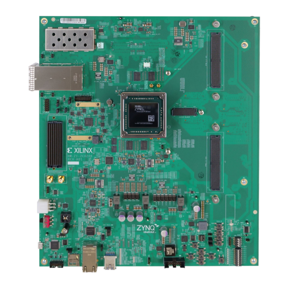
• Handle the devices carefully to prevent permanent damage. Board Component Location The following figure shows the ZCU208 board component locations. Each numbered component shown in the figure is keyed to Table UG1410 (v1.0) July 8, 2020 www.xilinx.com Send Feedback ZCU208 Board User Guide... - Page 12 Figure 2: ZCU208 Component Locations Round callout references a component Square callout references a component on the front side of the board on the back side of the board X23771-062520 UG1410 (v1.0) July 8, 2020 www.xilinx.com Send Feedback ZCU208 Board User Guide...
- Page 13 System controller (SC) TI MSP430F5342 MSP430 SC emulation cable connector TYCO 5103308-2 SW6, SW7 System controller 5-pole DIP switch and 5-pole C&K SDA05H1SBD, reset PB switch E-Switch TL3301EP100QG UG1410 (v1.0) July 8, 2020 www.xilinx.com Send Feedback ZCU208 Board User Guide...
- Page 14 INFINEON PMIC2 Infineon IRPS5401MXI04TRP INFINEON PMIC3 Infineon IRPS5401MXI04TRP U127 VCCINT PS/block RAM 18A regulator Infineon IR38164 U112 MGTAVCC 4A regulator Infineon IR38164 U123 VCC1V8 8A regulator Infineon IR38164 UG1410 (v1.0) July 8, 2020 www.xilinx.com Send Feedback ZCU208 Board User Guide...
-
Page 15: Default Jumper And Switch Settings
The following figure shows the ZCU208 board jumper header and switch locations. Each numbered component shown in the figure is keyed to the applicable table in this section. Both tables reference the respective schematic page numbers. UG1410 (v1.0) July 8, 2020 www.xilinx.com Send Feedback ZCU208 Board User Guide... - Page 16 Chapter 2: Board Setup and Configuration Figure 3: Board Jumper Header and Switch Locations X23508-062520 UG1410 (v1.0) July 8, 2020 www.xilinx.com Send Feedback ZCU208 Board User Guide...
- Page 17 2-3: J20 shield directly to GND SD3.0 U107 IP4856CX25 level-trans. ref. voltage select 1-2: Track SD3.0 J12 socket UTIL_3V3 3.3V 2-3: GND = revert to internal voltage reference UG1410 (v1.0) July 8, 2020 www.xilinx.com Send Feedback ZCU208 Board User Guide...
- Page 18 Switch OFF = 1 = High; ON = 0 = Low GPIO 8-pole DIP switch SW14 00000000 Switch OFF = 0 = Low; ON = 1 = High SW15 Main power slide switch UG1410 (v1.0) July 8, 2020 www.xilinx.com Send Feedback ZCU208 Board User Guide...
-
Page 19: Zynq Ultrascale+ Rfsoc Xczu48Dr
2. Set the boot mode pins SW2 [4:1] as indicated in the table above for QSPI32. 3. Either power-cycle or press the power-on reset (POR) pushbutton. SW2 is callout 11 in Figure Use the following steps to boot from an SD card. UG1410 (v1.0) July 8, 2020 www.xilinx.com Send Feedback ZCU208 Board User Guide... - Page 20 3. Either power-cycle or press the power-on reset (POR) pushbutton. SW2 is callout 11 in Figure See the Zynq UltraScale+ Device Technical Reference Manual (UG1085) for more information about Zynq UltraScale+ RFSoC configuration options. UG1410 (v1.0) July 8, 2020 www.xilinx.com Send Feedback ZCU208 Board User Guide...
-
Page 21: Chapter 3: Board Component Descriptions
UltraScale+ RFSoC Data Sheet: DC and AC Switching Characteristics (DS926) for more information. Top-level Block Diagram The following figure shows the top-level block diagram for the Zynq UltraScale+ RFSoC. UG1410 (v1.0) July 8, 2020 www.xilinx.com Send Feedback ZCU208 Board User Guide... - Page 22 Interlaken Ethernet SHA3 Quad Quad AES-GCM Processor System PCIe DDRC (DDR4/3/3L, LPDDR3/4) 128 KB RAM To ACP Gen4 32-bit/64-bit Battery Low Power Full Power Power 64-bit 128-bit X23642-033020 UG1410 (v1.0) July 8, 2020 www.xilinx.com Send Feedback ZCU208 Board User Guide...
- Page 23 Encryption Key Battery Backup Circuit The Zynq UltraScale+ RFSoC ZU48DR U1 implements bit stream encryption key technology. The ZCU208 board provides the encryption key backup battery circuit shown in the figure below. UG1410 (v1.0) July 8, 2020 www.xilinx.com Send Feedback ZCU208 Board User Guide...
- Page 24 VCC1V8 1.8V QSPI LWR/UPR, PS_GPIO2, MIO_I2C0/1, UART0, MIO_LED/PB PS Bank 501 VCC1V8 1.8V PMU_INPUT, PMU_GPO[0:5], SDIO I/F, PS_GPIO1 PS Bank 502 VCC1V8 1.8V USB (3.0) I/F, ENET I/F UG1410 (v1.0) July 8, 2020 www.xilinx.com Send Feedback ZCU208 Board User Guide...
- Page 25 Micron Technology website. The detailed RFSoC connections for the feature described in this section are documented in the ZCU208 board XDC file, referenced in Appendix B: Xilinx Design Constraints. UG1410 (v1.0) July 8, 2020 www.xilinx.com Send Feedback ZCU208 Board User Guide...
- Page 26 For additional details, see the Micron MT40A1G8SA-075 data sheet on the Micron Technology website. The detailed RFSoC connections for the feature described in this section are documented in the ZCU208 board XDC file, referenced in Appendix B: Xilinx Design Constraints. PL C1 I/F DDR4 Component Memory [Figure 2, callout 4] The 4 GB, 32-bit wide DDR4 memory system is comprised of four 1 Gb x 8 SDRAM (Micron MT40A1G8SA-075), U100-U103.
- Page 27 The detailed RFSoC connections for the feature described in this section are documented in the ZCU208 board XDC file, referenced in Appendix B: Xilinx Design Constraints. PSMIO The following table provides PS MIO peripheral mapping implemented on the ZCU208 board.
- Page 28 Micron MT25QU02GCBB8E12-0SIT data sheet on the Micron Technology website. The detailed RFSoC connections for the feature described in this section are documented in the ZCU208 board XDC file, referenced in Appendix B: Xilinx Design Constraints. UG1410 (v1.0) July 8, 2020 www.xilinx.com Send Feedback...
- Page 29 P1_6 AU26 MIO13_PS_GPIO2 P1_7 I2C Bus Topology Overview I2C0 (MIO 14-15), I2C1 (MIO 16-17) The following figure shows a high-level view of the I2C0 and I2C1 bus connectivity. UG1410 (v1.0) July 8, 2020 www.xilinx.com Send Feedback ZCU208 Board User Guide...
- Page 30 PMBUS power controllers and INA226 power monitors through the U17 PCA9544A switch. TCA6416A U15 is pin-strapped to respond to I2C address 0x20. The PCA9544A U17 switch is set to 0x75. UG1410 (v1.0) July 8, 2020 www.xilinx.com Send Feedback ZCU208 Board User Guide...
- Page 31 Schematic Net Name Reference Pin No. Pin No. Pin Name Device Name Designator I2C0_SDA Refer to connections shown in the figure above. TCA6416A U15 Addr. 0x20 I2C0_SCL MAX6643_OT_B OT_B MAX6643 UG1410 (v1.0) July 8, 2020 www.xilinx.com Send Feedback ZCU208 Board User Guide...
- Page 32 INA226_PMBus (Power Monitors) 0X40-0x43, 0x45-0x4E Not Connected IRPS5401_PMBus (Voltage Regulators) 0X40, 0x43, 0x44, 0x45, 0x4B, 0x4C SYSMON U1 bank 65 0X32 I2C1 (MIO 16-17) [Figure 2, callout 18] UG1410 (v1.0) July 8, 2020 www.xilinx.com Send Feedback ZCU208 Board User Guide...
- Page 33 Table 11: I2C1 TCA9548A U20 Target Device Addresses TCA9548A U20 (Addr 0x74) Port I2C1 Bus Device Target Device Address EEPROM U16 0X54 Si5341 Clock U43 0x76 USER Si570 C0 Clock U47 0X5D UG1410 (v1.0) July 8, 2020 www.xilinx.com Send Feedback ZCU208 Board User Guide...
- Page 34 For more information on the TCA9548A, TCA6416A, and PCA9544A, see the Texas Instruments website. The detailed Zynq UltraScale+ RFSoC connections for the feature described in this section are documented in the ZCU208 board XDC file, referenced in Appendix B: Xilinx Design Constraints. UART0 (MIO 18-19) [Figure 2, callout 8] This is the primary Zynq UltraScale+ RFSoC PS-side UART interface and is connected to the FTDI U29 FT4232HL USB-to-Quad-UART Bridge port B through TXS0108E level-shifter U32.
- Page 35 The detailed RFSoC connections for the feature described in this section are documented in the ZCU208 board XDC file, referenced in Appendix B: Xilinx Design Constraints. GPIO (MIO 22-23) PS-side pushbutton SW1 is connected to MIO22 (pin U1.AL27). PS-side LED DS1, physically placed adjacent to the pushbutton, is connected to MIO23 (pin U1.AM27).
- Page 36 The detailed RFSoC connections for the feature described in this section are documented in the ZCU208 board XDC file, referenced in Appendix B: Xilinx Design Constraints. SDIO (MIO 39-51) A PS-side interface to an SD card connector is provided for booting and file system storage. This interface is used for the SD boot mode and supports SD3.0 access post boot.
- Page 37 Table 15: IP4856CX25 U23 Adapter Pinout Aires Adapter Pin Number IP4856CX25 U23 Pin Number IP4856CX25 U23 Pin Name CLK_IN CMD_H CLK_FB VLDO VSD_REF DIR_0 VSUPPLY VCCA DIR_CMD DATA0_H UG1410 (v1.0) July 8, 2020 www.xilinx.com Send Feedback ZCU208 Board User Guide...
- Page 38 The detailed RFSoC connections for the feature described in this section are documented in the ZCU208 board XDC file, referenced in Appendix B: Xilinx Design Constraints. USB0 (MIO 52-63) USB 3.0 Transceiver and USB 2.0 The USB interface on the PS-side serves multiple roles as a host or device controller. The USB 3.0 interface (host mode only) is supported by the RFSoC GTR interface while the USB 2.0 (host...
- Page 39 DS7 is located adjacent to the USB J18 connector (Figure 2, callout 6). The following figure shows the ULPI U6 transceiver circuit. Figure 12: USB3320 ULPI USB 2.0 Transceiver Circuit UG1410 (v1.0) July 8, 2020 www.xilinx.com Send Feedback ZCU208 Board User Guide...
- Page 40 Chapter 3: Board Component Descriptions The detailed RFSoC connections for the feature described in this section are documented in the ZCU208 board XDC file, referenced in Appendix B: Xilinx Design Constraints. GEM3 Ethernet (MIO 64-77) [Figure 2, callout 16] The PS-side Gigabit Ethernet MAC (GEM) implements a 10/100/1000 Mb/s Ethernet interface, shown in the following figure, which connects to a TI DP83867IRPAP Ethernet RGMII PHY before being routed to an RJ45 Ethernet connector.
- Page 41 For more Ethernet PHY details, see the TI DS83867 data sheet on the Texas Instruments website. The detailed RFSoC connections for the feature described in this section are documented in the ZCU208 board XDC file, referenced in Appendix B: Xilinx Design Constraints. UG1410 (v1.0) July 8, 2020 www.xilinx.com Send Feedback...
- Page 42 Figure 15: JTAG Chain Block Diagram JTAG 2 mm 2X7 Header FT4232HL UART BRIDGE JTAG N.C. J28 (D) JTAG FMCP HSPC Connector PS Config Bank 503 JTAG X23652-012220 UG1410 (v1.0) July 8, 2020 www.xilinx.com Send Feedback ZCU208 Board User Guide...
- Page 43 U47 SI570 I2C Prog. Oscillator DDR4 C0 I/F (300 MHz default) U47.4 USER_SI570_C0_P LVDS AR20 U47.5 USER_SI570_C0_N LVDS AR19 U130 SI570 I2C Prog. Oscillator DDR4 C1 I/F (300 MHz default) U130.4 USER_SI570_C1_P LVDS U130.5 USER_SI570_C1_N LVDS UG1410 (v1.0) July 8, 2020 www.xilinx.com Send Feedback ZCU208 Board User Guide...
- Page 44 • Differential and single-ended outputs The SI5341B data sheet addendum for the Silicon Labs SI5341B-D07833-GM documents the pre-programmed output frequencies: • Inputs: XAXB: 48 MHz ○ Crystal mode ○ IN0: Unused ○ UG1410 (v1.0) July 8, 2020 www.xilinx.com Send Feedback ZCU208 Board User Guide...
- Page 45 Bank 69 I/F C1: U130) and one assigned to GTY131 (U48). On power-up the user clocks default to a pre-programmed output frequency: DDR4 I/F U47 and U130 to 300.000 MHz and GTY I/F U48 to 156.250 MHz. UG1410 (v1.0) July 8, 2020 www.xilinx.com Send Feedback ZCU208 Board User Guide...
- Page 46 U1 MGTREFCLK1N pin M35. The user SMA MGT clock differential signal amplitude must not exceed -0.5V (Min) to 1.30V (Max). The detailed RFSoC connections for the feature described in this section are documented in the ZCU208 board XDC file, referenced in Appendix B: Xilinx Design Constraints. zSFP/zSFP+ Module Connectors [Figure 2, callout 15] UG1410 (v1.0) July 8, 2020...
- Page 47 X24156-062520 The detailed RFSoC connections for the feature described in this section are documented in the ZCU208 board XDC file, referenced in Appendix B: Xilinx Design Constraints. The following table lists the zSFP+ module control and status connections. Table 19: zSFP Control and Status Board Connections...
- Page 48 BW selection is also available through I2C control. For additional information about the zSFP module, see SFF-8402 and SFF-8432 on the SNIA Technology Affiliates website. UG1410 (v1.0) July 8, 2020 www.xilinx.com Send Feedback ZCU208 Board User Guide...
- Page 49 CPU_RESET: SW13 ○ The detailed RFSoC connections for the feature described in this section are documented in the ZCU208 board XDC file, referenced in Appendix B: Xilinx Design Constraints. Power and Status LEDs [Figure 2, area of callouts 17 and 18] The following table defines the power and status LEDs.
- Page 50 PL_C0_DDR4_VTERM_ Green PL_C0_DDR4_VTERM 0.6VDC power on 0V60_PG DS43 PL_C1_DDR4_VTERM_ Green PL_C1_DDR4_VTERM 0.6VDC power on 0V60_PG DS44 DAC_AVCCAUX_ON Green DAC_AVCCAUX 1.8VDC power on DS46 LED_0 Green USER GPIO LED_0 UG1410 (v1.0) July 8, 2020 www.xilinx.com Send Feedback ZCU208 Board User Guide...
- Page 51 DS53 LED_7 Green USER GPIO LED_7 The following figure shows the GPIO and power status LED areas of the board. Figure 17: GPIO and Power Status LED areas UG1410 (v1.0) July 8, 2020 www.xilinx.com Send Feedback ZCU208 Board User Guide...
- Page 52 GTY Quad 130 ILKN FMC DP0 USER_SMA_MGT_CLOCK refclk1 FMC GBTCLK0 M2C refclk0 FMC DP7 FMC DP6 FMC DP5 GTY Quad 131 PCIe4 FMC DP4 USER_MGT_SI570_CLOCK refclk1 FMC GBTCLK1 M2C refclk0 UG1410 (v1.0) July 8, 2020 www.xilinx.com Send Feedback ZCU208 Board User Guide...
- Page 53 User Guide (UG578). The detailed RFSoC connections for the feature described in this section are documented in the ZCU208 board XDC file, referenced in Appendix B: Xilinx Design Constraints. PS GTR Transceivers The PS-side GTR transceiver Bank 505 supports USB (3.0) and SATA, with two channels not used.
- Page 54 ADD_IN CARD KEY M ADD_IN CARD KEY M ADD_IN CARD KEY M ADD_IN CARD KEY M Reserved for MFG_CLOCK ADD_IN CARD KEY M Reserved for MFG_DATA SATA-A+ SATA-A- ALERT# (O) (0/1.8V) UG1410 (v1.0) July 8, 2020 www.xilinx.com Send Feedback ZCU208 Board User Guide...
- Page 55 DNP Res to GND PEDET No Connect SATA-A GTR TX 49, 47 SATA-B GTR RX 43, 41 The M.2 U40 connector to RFSoC connections are listed in the following table. UG1410 (v1.0) July 8, 2020 www.xilinx.com Send Feedback ZCU208 Board User Guide...
- Page 56 The detailed RFSoC connections for the feature described in this section are documented in the ZCU208 board XDC file, referenced in Appendix B: Xilinx Design Constraints. FPGA Mezzanine Card Interface The ZCU208 evaluation board supports the VITA 57.4 FPGA mezzanine card plus (FMC+ or FMCP) specification by providing a subset implementation of the high pin count connector at J28 (HSPC).
- Page 57 Alliance website for additional information on the FMCP HSPC connector. The detailed RFSoC connections for the feature described in this section are documented in the ZCU208 board XDC file, referenced in Appendix B: Xilinx Design Constraints. Cooling Fan Connector [Figure...
- Page 58 The ZCU208 website also includes the ZCU208 System Controller GUI Tutorial (XTP_TBD) and ZCU208 Software Install and Board Setup Tutorial (XTP_TBD). These steps briefly summarize these instructions. UG1410 (v1.0) July 8, 2020 www.xilinx.com Send Feedback ZCU208 Board User Guide...
- Page 59 • SW15 power on/off slide switch (callout 24) • SW3 (PS_PROG_B), active-Low pushbutton (callout 23) • SW4 (POR_B), active-Low pushbutton (callout 23) • SW5 (SRST_B), active-Low pushbutton (callout 23) UG1410 (v1.0) July 8, 2020 www.xilinx.com Send Feedback ZCU208 Board User Guide...
- Page 60 See the Zynq UltraScale+ Device Technical Reference Manual (UG1085) for information about the Zynq UltraScale+ RFSoC configuration. System Reset Pushbuttons [Figure 2, callout 23] The following figure shows the reset circuitry for the processing system. UG1410 (v1.0) July 8, 2020 www.xilinx.com Send Feedback ZCU208 Board User Guide...
- Page 61 The ZCU208 evaluation board uses power management ICs (PMIC) and regulators from Infineon Integrated Circuits to supply the core and auxiliary voltages listed in the following table. Reference schematic 038-05003-01. UG1410 (v1.0) July 8, 2020 www.xilinx.com Send Feedback ZCU208 Board User Guide...
- Page 62 Non-PMBus ADC and DAC voltage regulator data sheets can be viewed on the website. The PCB layout and power system design meet the recommended criteria described in the UltraScale Architecture PCB Design User Guide (UG583). UG1410 (v1.0) July 8, 2020 www.xilinx.com Send Feedback ZCU208 Board User Guide...
- Page 63 Chapter 3: Board Component Descriptions report_power command in RECOMMENDED: To ensure reliable operation, Xilinx recommends running the the Vivado tools for designs targeting this board. The reported rail current requirements must not exceed the values listed in the following table.
- Page 64 INA226 power monitor op amps. Also refer to schematic 038-05003-01. Power rail measurements are accessible to the system controller and RFSoC PL logic through their respective I2C0 bus connections. UG1410 (v1.0) July 8, 2020 www.xilinx.com Send Feedback ZCU208 Board User Guide...
-
Page 65: Appendix A: Vita57.4 Fmcp Connector Pinout
(HSPC) connector defined by the VITA 57.4 FMC specification. For a description of how the ZCU208 evaluation board implements the FMCP specification, see FPGA Mezzanine Card Interface. Figure 22: FMCP HSPC Connector Pinout UG1410 (v1.0) July 8, 2020 www.xilinx.com Send Feedback ZCU208 Board User Guide... -
Page 66: Appendix B: Xilinx Design Constraints
Xilinx Design Constraints Overview The Xilinx design constraints (XDC) file template for the ZCU208 board provides for designs targeting the ZCU208 evaluation board. Net names in the constraints listed correlate with net names on the latest ZCU208 evaluation board schematic. Identify the appropriate pins and replace the net names with net names in the user RTL. -
Page 67: Appendix C: Hw-Xm650/655 Balun Daughter Cards For Gen 3 Rfsoc Evm
Balun XM650: N79 or B46 band with BOM change XM655: Low/mid/high frequency Filter XM650: N79 or B46 band with BOM change XM655: No Interconnection 2x Samtec LPAM 8x50 UG1410 (v1.0) July 8, 2020 www.xilinx.com Send Feedback ZCU208 Board User Guide... -
Page 68: Block Diagram
Appendix C: HW-XM650/655 Balun Daughter Cards for Gen 3 RFSoC EVM Block Diagram XM655: 16T16R Breakout Add-on Card Figure 23: XM655 Block Diagram XM650: 16T16R N79 Band Loopback Demo Add-on Card Figure 24: XM650 Block Diagram UG1410 (v1.0) July 8, 2020 www.xilinx.com Send Feedback ZCU208 Board User Guide... -
Page 69: Connector
Stack height .157"/4.00 mm (Mated with LPAF-50-03.0-L-08-2-K-TR) Make SAMTEC Description Low profile open pin field array, male connector Data sheet See the Samtec website Figure 25: LPAM-50-01.0-L-08-2-K-TR 3D View UG1410 (v1.0) July 8, 2020 www.xilinx.com Send Feedback ZCU208 Board User Guide... -
Page 70: Xm650/655 Connector Pinout
DACIO_VADJ DAC_AVTT Spare 1 DACIO_00 DACIO_04 DACIO_08 DACIO_12 DACIO_02 DACIO_06 DACIO_10 DACIO_14 DACIO_01 DACIO_05 DACIO_09 DACIO_13 DACIO_03 DACIO_07 DACIO_11 DACIO_15 DAC231_T3_ DAC231_T3_ CH3_N CH3_P DAC231_T3_ DAC231_T3_ CH2_N CH2_P UG1410 (v1.0) July 8, 2020 www.xilinx.com Send Feedback ZCU208 Board User Guide... - Page 71 DAC229_T1_ DAC229_T1_ CH3_N CH3_P DAC229_T1_ DAC229_T1_ CH2_N CH2_P DAC229_T1_ DAC229_T1_ CH1_N CH1_P DAC229_T1_ DAC229_T1_ CH0_N CH0_P DAC228_T0_ DAC228_T0_ CH3_N CH3_P DAC228_T0_ DAC228_T0_ CH2_N CH2_P DAC228_T0_ DAC228_T0_ CH1_N CH1_P UG1410 (v1.0) July 8, 2020 www.xilinx.com Send Feedback ZCU208 Board User Guide...
- Page 72 ADC226_T2_ ADC226_T2_ CH3_N CH3_P ADC226_T2_ ADC226_T2_ CH2_N CH2_P ADC226_T2_ ADC226_T2_ CH1_N CH1_P ADC226_T2_ ADC226_T2_ CH0_N CH0_P ADC225_T1_ ADC225_T1_ CH3_N CH3_P ADC225_T1_ ADC225_T1_ CH2_N CH2_P ADC225_T1_ ADC225_T1_ CH1_N CH1_P UG1410 (v1.0) July 8, 2020 www.xilinx.com Send Feedback ZCU208 Board User Guide...
- Page 73 VCM_ADC22 VCM_ADC22 VCM_ADC22 VCM_ADC22 4_T0_CH01 5_T1_CH01 6_T2_CH01 7_T3_CH01 ADCIO_02 ADCIO_06 ADCIO_10 ADCIO_14 ADCIO_00 ADCIO_04 ADCIO_08 ADCIO_12 ADCIO_03 ADCIO_07 ADCIO_11 ADCIO_15 ADCIO_01 ADCIO_05 ADCIO_09 ADCIO_13 I2C_SCL I2C_SDA ADCIO_VADJ ADCIO_VADJ UG1410 (v1.0) July 8, 2020 www.xilinx.com Send Feedback ZCU208 Board User Guide...
-
Page 74: Corehc2 Connector Pin Out (Xm655 Only)
Figure 27: ADC 16 Lanes JHC5 JHC6 ADC224_T0_CH0 Tile Channel ADC224_T0_CH1 ADC224_T0_CH2 ADC224_T0_CH3 ADC225_T1_CH0 ADC225_T1_CH1 ADC225_T1_CH2 ADC225_T1_CH3 ADC226_T2_CH0 ADC226_T2_CH1 ADC226_T2_CH2 ADC226_T2_CH3 ADC227_T3_CH0 ADC227_T3_CH1 ADC227_T3_CH2 ADC227_T3_CH3 JHC7 JHC8 X24154-062520 UG1410 (v1.0) July 8, 2020 www.xilinx.com Send Feedback ZCU208 Board User Guide... -
Page 75: Features
• 2 ADC inputs – compression mount SMAs through low frequency baluns – Minicircuits TCM2-33WX+ • 2 ADC inputs – compression mount SMAs through mid frequency baluns – Anaren BD1631J50100AHF UG1410 (v1.0) July 8, 2020 www.xilinx.com Send Feedback ZCU208 Board User Guide... -
Page 76: Board Specifications
When the module is mated with ZCU208 RFMC 2.0 connectors (Samtec LPAF-50-03.0-L-08-2- K-TR), the mated height between the boards will be 4.0 mm. No component is placed on the bottom side of the module. UG1410 (v1.0) July 8, 2020 www.xilinx.com Send Feedback ZCU208 Board User Guide... - Page 77 Appendix C: HW-XM650/655 Balun Daughter Cards for Gen 3 RFSoC EVM • XM655 Dimensions: Length: 9.85" (250.19 mm) Width: 4.90" (124.46 mm) Thickness: 0.065" (1.651 mm) UG1410 (v1.0) July 8, 2020 www.xilinx.com Send Feedback ZCU208 Board User Guide...
- Page 78 Appendix C: HW-XM650/655 Balun Daughter Cards for Gen 3 RFSoC EVM Figure 29: XM655 Board Dimensions • XM650 Dimensions: Length: 9.85" (250.19 mm) UG1410 (v1.0) July 8, 2020 www.xilinx.com Send Feedback ZCU208 Board User Guide...
- Page 79 Mounting Holes/Keepouts There are four jack screws on the module and two edge standoff, as shown in the figure above. The boards are screwed to the ZCU208 board. UG1410 (v1.0) July 8, 2020 www.xilinx.com Send Feedback ZCU208 Board User Guide...
-
Page 80: Functional Description
See the Samtec website – Functional Description Cables/SMAs XM655 Cables: Carlisle Core HC2 8 Channel – Male, 3.5 mm TM40-0157-00 Figure 31: Carlisle Core HC2 8 Channel–Male Cable UG1410 (v1.0) July 8, 2020 www.xilinx.com Send Feedback ZCU208 Board User Guide... - Page 81 Appendix C: HW-XM650/655 Balun Daughter Cards for Gen 3 RFSoC EVM Figure 32: TM40-0157-00 Landing Pad O .085[2.150] O .012+001[0:] 070± 0.025 .530± 0.013 .016[0.411] .031[0.790] .024[0.600] .024[0.600] .078[1.986] X23659-041420 SMAs: Carlisle Compression – Mount SMA, TMB-V5F2-1L1 UG1410 (v1.0) July 8, 2020 www.xilinx.com Send Feedback ZCU208 Board User Guide...
- Page 82 Appendix C: HW-XM650/655 Balun Daughter Cards for Gen 3 RFSoC EVM Figure 33: TMB-V5F2-1L1 SMA Drawing Figure 34: SMA to SMA Cable: Carlisle TM40-0159-00 6" UG1410 (v1.0) July 8, 2020 www.xilinx.com Send Feedback ZCU208 Board User Guide...
- Page 83 — 3000 Insertion loss 10-3000 — Amplitude unbalance 10-3000 — — Phase unbalance 10-3000 — — Degree Notes: Insertion loss is reference to mid-band loss, 0.8 dB typ. UG1410 (v1.0) July 8, 2020 www.xilinx.com Send Feedback ZCU208 Board User Guide...
- Page 84 Table 33: Medium Frequency Balun Part Number Parameter Value Part number BD1631J50100AHF Manufacturer Anaren Order P/N 1173-1059-2-ND Vendor Digikey Description Balun 1.6 GHZ-3.1 GHZ 50/100 0805 Data sheet See the Anaren website UG1410 (v1.0) July 8, 2020 www.xilinx.com Send Feedback ZCU208 Board User Guide...
- Page 85 Table 34: High Frequency Balun (4-5 GHz) Part Number Parameter Value Part number BD3150N50100AHF Manufacturer Anaren Order P/N 1173-1069-2-ND Vendor Digikey Description Balun 3.1 GHZ-5 GHZ 50/100 0404 Data sheet See the Anaren website UG1410 (v1.0) July 8, 2020 www.xilinx.com Send Feedback ZCU208 Board User Guide...
- Page 86 Table 35: High Frequency Balun (5-6 GHz) Part Number Parameter Value Part number BD4859N50100AHF Manufacturer Anaren Order P/N 1173-1070-2-ND Vendor Digikey Description BALUN 4.8 GHz-5.9 GHz 50/100 0404 Data sheet See the Anaren website UG1410 (v1.0) July 8, 2020 www.xilinx.com Send Feedback ZCU208 Board User Guide...
- Page 87 Table 36: RF Cages Parameter Value Part number LT-7925 Manufacturer Leader Tech Order P/N LT-7925 Vendor Leader Tech Description EMI cage Data sheet See the Leader Tech website UG1410 (v1.0) July 8, 2020 www.xilinx.com Send Feedback ZCU208 Board User Guide...
- Page 88 Chip multilayer Balun 4.4 GHz~5 GHz Data sheet See the Murata website Header There are a total of 20 DACIO and 20 ADCIO digital I/O pins on the header strips. UG1410 (v1.0) July 8, 2020 www.xilinx.com Send Feedback ZCU208 Board User Guide...
- Page 89 Appendix C: HW-XM650/655 Balun Daughter Cards for Gen 3 RFSoC EVM Figure 42: High ADCIO and DACIO Digital I/O Header Pins UG1410 (v1.0) July 8, 2020 www.xilinx.com Send Feedback ZCU208 Board User Guide...
-
Page 90: Appendix D: Additional Resources And Legal Notices
• On Windows, select Start → All Programs → Xilinx Design Tools → DocNav. • At the Linux command prompt, enter docnav. Xilinx Design Hubs provide links to documentation organized by design tasks and other topics, which you can use to learn key concepts and address frequently asked questions. To access the Design Hubs: •... - Page 91 Infineon Integrated Circuits (IR35215, IRPS5401, IR38164, IR3889, IR3897) Monolithic Power Systems (MPM3683, MPM3833) Future Technology Devices International Ltd. (FT4232HL) SNIA Technology Affiliates (SFF-8402, SFF-8432) Nexperia/NXP Semiconductors (IP4856CX25, SC18IS602) UG1410 (v1.0) July 8, 2020 www.xilinx.com Send Feedback ZCU208 Board User Guide...
-
Page 92: Please Read: Important Legal Notices
IP cores may be subject to warranty and support terms contained in a license issued to you by Xilinx. Xilinx products are not designed or intended to be fail-safe or for use in any application requiring fail-safe performance; you assume sole risk and liability for...
Need help?
Do you have a question about the Zynq UltraScale+ ZCU208 and is the answer not in the manual?
Questions and answers