Table of Contents
Advertisement
Advertisement
Table of Contents

Subscribe to Our Youtube Channel
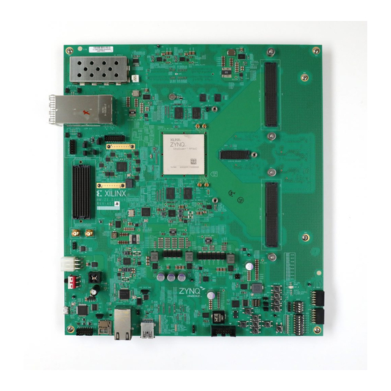
Related Manuals for Xilinx Zynq UltraScale+ ZCU216


Summary of Contents for Xilinx Zynq UltraScale+ ZCU216
- Page 1 ZCU216 Evaluation Board User Guide UG1390 (v1.1) July 10, 2020...
- Page 2 Chapter 3: Board Component Descriptions ........... 22 Overview.............................22 Component Descriptions......................22 Appendix A: VITA 57.4 FMCP Connector Pinout ........... 68 Overview.............................68 Appendix B: Xilinx Design Constraints ............. 69 Overview.............................69 Appendix C: XM650/XM655 Balun Add-on Cards for RFSoC EVM ..70 Overview.............................70 Block Diagram........................... 71 Connector...........................72...
- Page 3 Appendix D: Regulatory and Compliance Information ......92 CE Information...........................92 Compliance Markings....................... 93 Appendix E: Additional Resources and Legal Notices ......94 Xilinx Resources.........................94 Documentation Navigator and Design Hubs.................94 References..........................94 Please Read: Important Legal Notices................... 96 UG1390 (v1.1) July 10, 2020 www.xilinx.com...
- Page 4 The following table shows the revision history for this document. Section Revision Summary 07/10/2020 Version 1.1 XM650/655 Connector Pinout Revised connector pinout tables. 03/17/2020 Version 1.0 Initial release. UG1390 (v1.1) July 10, 2020 www.xilinx.com Send Feedback ZCU216 Board User Guide...
- Page 5 ZCU216 evaluation board. Block Diagram A block diagram of the ZCU216 evaluation board is shown in the following figure. UG1390 (v1.1) July 10, 2020 www.xilinx.com Send Feedback ZCU216 Board User Guide...
- Page 6 The ZCU216 evaluation board features are listed here. Detailed information for each feature is provided in Chapter 3: Board Component Descriptions. • XCZU49DR-2, FFVF1760 package • Form factor: See Board Specifications • Configuration from: Dual QSPI ○ Micro-SD card ○ UG1390 (v1.1) July 10, 2020 www.xilinx.com Send Feedback ZCU216 Board User Guide...
- Page 7 DAC_CLK_229 (direct connect SMAs) ○ USER_MGT_SMA_CLK (series capacitor connected SMAs) ○ • PS DDR4 4 GB 64-bit SODIMM • PL DDR4 C0 I/F 2 GB 32-bit Component (4x8-bit) UG1390 (v1.1) July 10, 2020 www.xilinx.com Send Feedback ZCU216 Board User Guide...
- Page 8 PS MIO[52:63]: USB3.0 ○ PS MIO[64:77]: Ethernet RGMII ○ • PL I/O Connections: PL User DIP switch (8-position) ○ PL User pushbuttons (5, Geographic N, S, E, W, C) ○ UG1390 (v1.1) July 10, 2020 www.xilinx.com Send Feedback ZCU216 Board User Guide...
- Page 9 Block RAM Blocks 1080 (38 Mb) UltraRAM Blocks 80 (22.5 Mb) DSP Slices 4,272 PCIe ® Gen3 x16 / Gen4 x8 / CCIX (3) 150G Interlaken 100G Ethernet w/ RS-FEC UG1390 (v1.1) July 10, 2020 www.xilinx.com Send Feedback ZCU216 Board User Guide...
- Page 10 XDC listing and board schematics. Environmental • Temperature: Operating: 0°C to +45°C Storage: –25°C to +60°C • Humidity: 10% to 90% non-condensing Operating Voltage +12 V UG1390 (v1.1) July 10, 2020 www.xilinx.com Send Feedback ZCU216 Board User Guide...
- Page 11 • Handle the devices carefully to prevent permanent damage. Board Component Location The following figure shows the ZCU216 board component locations. Each numbered component shown in the figure is keyed to Table UG1390 (v1.1) July 10, 2020 www.xilinx.com Send Feedback ZCU216 Board User Guide...
- Page 12 Always refer to the schematic, layout, and XDC files of the specific ZCU216 version of interest for such details. UG1390 (v1.1) July 10, 2020 www.xilinx.com Send Feedback ZCU216 Board User Guide...
- Page 13 Figure 2: ZCU216 Component Locations Round callout references a component Square callout references a component on the front side of the board on the back side of the board X23462-111419 UG1390 (v1.1) July 10, 2020 www.xilinx.com Send Feedback ZCU216 Board User Guide...
- Page 14 MSP430 SC Emulation Cable Connector TYCO 5103308-2 SW6, SW7 System Controller 5-pole DIP Switch and 5-pole C&K SDA05H1SBD, Reset PB Switch E-Switch TL3301EP100QG J46, J47 PMOD0/1 RA Receptacles SULLINS PPPC062LJBN-RC UG1390 (v1.1) July 10, 2020 www.xilinx.com Send Feedback ZCU216 Board User Guide...
- Page 15 Infineon IR35215MTRPBF INFINEON PMIC2 Infineon IRPS5401MXI04TRP INFINEON PMIC3 Infineon IRPS5401MXI04TRP U127 VCCINT PS/BRAM 18A Regulator Infineon IR38164 U112 MGTAVCC 4A Regulator Infineon IR38164 U123 VCC1V8 8A Regulator Infineon IR38164 UG1390 (v1.1) July 10, 2020 www.xilinx.com Send Feedback ZCU216 Board User Guide...
- Page 16 The following figure shows the ZCU216 board jumper header and switch locations. Each numbered component shown in the figure is keyed to the applicable table in this section. Both tables reference the respective schematic page numbers. UG1390 (v1.1) July 10, 2020 www.xilinx.com Send Feedback ZCU216 Board User Guide...
- Page 17 Chapter 2: Board Setup and Configuration Figure 3: Board Jumper Header and Switch Locations X23508-111119 Jumpers The following table lists the default jumper settings. UG1390 (v1.1) July 10, 2020 www.xilinx.com Send Feedback ZCU216 Board User Guide...
- Page 18 1-2: Track SD3.0 J12 socket UTIL_3V3 3.3V 2-3: GND = revert to internal voltage reference MPS430 U38 RST_B and TEST pin options 1-2: MSP430_RST_B connected to PMOD1_0 open 3-4: MSP430_TEST connected to PMOD1_1 open UG1390 (v1.1) July 10, 2020 www.xilinx.com Send Feedback ZCU216 Board User Guide...
- Page 19 Switch OFF = 1 = High; ON = 0 = Low GPIO 8-Pole DIP Switch SW14 00000000 Switch OFF = 0 = Low; ON = 1 = High SW15 Main Power Slide Switch UG1390 (v1.1) July 10, 2020 www.xilinx.com Send Feedback ZCU216 Board User Guide...
- Page 20 2. Set the boot mode pins SW2 [4:1] as indicated in the table above for QSPI32. 3. Either power-cycle or press the power-on reset (POR) pushbutton. SW2 is callout 11 in Figure UG1390 (v1.1) July 10, 2020 www.xilinx.com Send Feedback ZCU216 Board User Guide...
- Page 21 3. Either power-cycle or press the power-on reset (POR) pushbutton. SW2 is callout 11 in Figure See the Zynq UltraScale+ Device Technical Reference Manual (UG1085) for more information about Zynq UltraScale+ RFSoC configuration options. UG1390 (v1.1) July 10, 2020 www.xilinx.com Send Feedback ZCU216 Board User Guide...
- Page 22 CCINT whichever Zynq UltraScale+ RFSoC speed grade is on the evaluation board. See the Zynq UltraScale+ RFSoC Data Sheet: DC and AC Switching Characteristics (DS926) for more information. UG1390 (v1.1) July 10, 2020 www.xilinx.com Send Feedback ZCU216 Board User Guide...
- Page 23 Interlaken Ethernet SHA3 Quad Quad AES-GCM Processor System PCIe 128 KB RAM DDRC (DDR4/3/3L, LPDDR3/4) To ACP Gen4 32-bit/64-bit Battery Low Power Full Power Power 64-bit 128-bit X23309-031220 UG1390 (v1.1) July 10, 2020 www.xilinx.com Send Feedback ZCU216 Board User Guide...
- Page 24 Encryption Key Battery Backup Circuit The Zynq UltraScale+ RFSoC ZU49DR U1 implements bit stream encryption key technology. The ZCU216 board provides the encryption key backup battery circuit shown in the figure below. UG1390 (v1.1) July 10, 2020 www.xilinx.com Send Feedback ZCU216 Board User Guide...
- Page 25 VCC1V8 1.8V QSPI LWR/UPR, PS_GPIO2, MIO_I2C0/1, UART0, MIO_LED/PB PS Bank 501 VCC1V8 1.8V PMU_INPUT, PMU_GPO[0:5], SDIO I/F, PS_GPIO1 PS Bank 502 VCC1V8 1.8V USB (3.0) I/F, ENET I/F UG1390 (v1.1) July 10, 2020 www.xilinx.com Send Feedback ZCU216 Board User Guide...
- Page 26 Micron Technology website. The detailed RFSoC connections for the feature described in this section are documented in the ZCU216 board XDC file, referenced in Appendix B: Xilinx Design Constraints. UG1390 (v1.1) July 10, 2020 www.xilinx.com Send Feedback ZCU216 Board User Guide...
- Page 27 For additional details, see the Micron MT40A1GWE-075E data sheet on the Micron Technology website. The detailed RFSoC connections for the feature described in this section are documented in the ZCU216 board XDC file, referenced in Appendix B: Xilinx Design Constraints. PL C1 I/F DDR4 Component Memory [Figure 2, callout 4] The 4 GB, 32-bit wide DDR4 memory system is comprised of four 1 Gb x 8 SDRAM (Micron MT40A1G8WE-075E), U100-U103.
- Page 28 The detailed RFSoC connections for the feature described in this section are documented in the ZCU216 board XDC file, referenced in Appendix B: Xilinx Design Constraints. PSMIO The following table provides PS MIO peripheral mapping implemented on the ZCU216 board.
- Page 29 Micron MT25QU02GCBB8E12-0SIT data sheet on the Micron Technology website. The detailed RFSoC connections for the feature described in this section are documented in the ZCU216 board XDC file, referenced in Appendix B: Xilinx Design Constraints. UG1390 (v1.1) July 10, 2020 www.xilinx.com Send Feedback...
- Page 30 P1_6 AU26 MIO13_PS_GPIO2 P1_7 I2C Bus Topology Overview I2C0 (MIO 14-15), I2C1 (MIO 16-17) The following figure shows a high-level view of the I2C0 and I2C1 bus connectivity. UG1390 (v1.1) July 10, 2020 www.xilinx.com Send Feedback ZCU216 Board User Guide...
- Page 31 PMBUS power controllers and INA226 power monitors through the U17 PCA9544A switch. TCA6416A U15 is pin-strapped to respond to I2C address 0x20. The PCA9544A U17 switch is set to 0x75. UG1390 (v1.1) July 10, 2020 www.xilinx.com Send Feedback ZCU216 Board User Guide...
- Page 32 Pin No. Pin No. Pin Name Device Name Designator I2C0_SDA Refer to connections shown in the figure above. TCA6416A U15 Addr. 0x20 I2C0_SCL MAX6643_OT_B OT_B MAX6643 MAX6643_FANFAIL_B FANFAIL_B MAX6643 UG1390 (v1.1) July 10, 2020 www.xilinx.com Send Feedback ZCU216 Board User Guide...
- Page 33 I2C switches (TCA9548A U20 and U22). These I2C1 connections enable I2C communications with various I2C capable target devices. TCA9548A U20 is pin-strapped to respond to I2C address 0x74. TCA9548A U22 is pin-strapped to respond to I2C address 0x75. UG1390 (v1.1) July 10, 2020 www.xilinx.com Send Feedback ZCU216 Board User Guide...
- Page 34 0x76 USER Si570 C0 Clock U47 0X5D USER MGT Si570 Clock U48 0X5D 8A34001 (zSFP ClK Recovery) U409 0x58 CLK104 Connector J101 0x2F RFMC LPAF-50 Connector J82 USER UG1390 (v1.1) July 10, 2020 www.xilinx.com Send Feedback ZCU216 Board User Guide...
- Page 35 For more information on the TCA9548A, TCA6416A, and PCA9544A, see the Texas Instruments website. The detailed Zynq UltraScale+ RFSoC connections for the feature described in this section are documented in the ZCU216 board XDC file, referenced in Appendix B: Xilinx Design Constraints. UART0 (MIO 18-19) [Figure 2, callout 8] This is the primary Zynq UltraScale+ RFSoC PS-side UART interface and is connected to the FTDI U29 FT4232HL USB-to-Quad-UART Bridge port B through TXS0108E level-shifter U32.
- Page 36 The detailed RFSoC connections for the feature described in this section are documented in the ZCU216 board XDC file, referenced in Appendix B: Xilinx Design Constraints. GPIO (MIO 22-23) PS-side pushbutton SW1 is connected to MIO22 (pin U1.AL27). PS-side LED DS1, physically placed adjacent to the pushbutton, is connected to MIO23 (pin U1.AM27).
- Page 37 The detailed RFSoC connections for the feature described in this section are documented in the ZCU216 board XDC file, referenced in Appendix B: Xilinx Design Constraints. SDIO (MIO 39-51) A PS-side interface to an SD card connector is provided for booting and file system storage. This interface is used for the SD boot mode and supports SD3.0 access post boot.
- Page 38 Aires Adapter Pin Number IP4856CX25 U23 Pin Number IP4856CX25 U23 Pin Name CLK_IN CMD_H CLK_FB VLDO VSD_REF DIR_0 VSUPPLY VCCA DIR_CMD DATA0_H DATA3_H DATA1_H DIR_1_3 DATA2_H DATA1_SD DATA0_SD CLK_SD UG1390 (v1.1) July 10, 2020 www.xilinx.com Send Feedback ZCU216 Board User Guide...
- Page 39 For more information on the IP4856CX25, see the website. The detailed RFSoC connections for the feature described in this section are documented in the ZCU216 board XDC file, referenced in Appendix B: Xilinx Design Constraints. USB0 (MIO 52-63) USB 3.0 Transceiver and USB 2.0 ULPI PHY The USB interface on the PS-side serves multiple roles as a host or device controller.
- Page 40 2, which will turn on LED DS7 if overcurrent or thermal shutdown conditions are detected. DS7 is located adjacent to the USB J18 connector (Figure 2, callout 6). The following figure shows the ULPI U6 transceiver circuit. UG1390 (v1.1) July 10, 2020 www.xilinx.com Send Feedback ZCU216 Board User Guide...
- Page 41 Chapter 3: Board Component Descriptions Figure 12: USB3320 ULPI USB 2.0 Transceiver Circuit The detailed RFSoC connections for the feature described in this section are documented in the ZCU216 board XDC file, referenced in Appendix B: Xilinx Design Constraints. GEM3 Ethernet (MIO 64-77) [Figure...
- Page 42 Note: This pin is a strap configuration pin for RGZ devices only. By default, this pin indicates that 100BASE-T link is established. LED_1 S, I/O, PD Additional functionality is configurable by means of LEDCR1[7:4] register bits. UG1390 (v1.1) July 10, 2020 www.xilinx.com Send Feedback ZCU216 Board User Guide...
- Page 43 Texas Instruments website. The detailed RFSoC connections for the feature described in this section are documented in the ZCU216 board XDC file, referenced in Appendix B: Xilinx Design Constraints. Programmable Logic JTAG Programming Options [Figure 2, callouts 8 and 9] ZCU216 JTAG chain: •...
- Page 44 X23321-100119 Clock Generation The ZCU216 board provides fixed and variable clock sources for the ZU49DR Zynq UltraScale+ RFSoC. The following table lists the source devices for each clock. UG1390 (v1.1) July 10, 2020 www.xilinx.com Send Feedback ZCU216 Board User Guide...
- Page 45 U130 SI570 I2C Prog. Oscillator DDR4 C1 I/F (300 MHz default) U130.4 USER_SI570_C1_P LVDS U130.5 USER_SI570_C1_N LVDS U49 SI570 I2C Prog. Oscillator (156.250 MHz default) U48.4 USER_MGT_SI570_CLOCK_P U48.5 USER_MGT_SI570_CLOCK_N J79 (P)/J80 (N) SMA Connectors USER_SMA_MGT_CLOCK_P UG1390 (v1.1) July 10, 2020 www.xilinx.com Send Feedback ZCU216 Board User Guide...
- Page 46 The SI5341B data sheet addendum for the Silicon Labs SI5341B-D07833-GM documents the pre-programmed output frequencies: • Inputs: XAXB: 48 MHz ○ Crystal Mode ○ IN0: Unused ○ IN1: Unused ○ IN2: Unused ○ FB_IN: Unused ○ UG1390 (v1.1) July 10, 2020 www.xilinx.com Send Feedback ZCU216 Board User Guide...
- Page 47 User applications can change the output frequency of each SI570 within the range of 10 MHz to 810 MHz through the I2C1 bus interface. Power cycling the ZCU216 board reverts user clocks to their default settings. UG1390 (v1.1) July 10, 2020 www.xilinx.com Send Feedback ZCU216 Board User Guide...
- Page 48 U1 MGTREFCLK1N pin M35. The user SMA MGT clock differential signal amplitude must not exceed -0.5V (Min) to 1.30V (Max). The detailed RFSoC connections for the feature described in this section are documented in the ZCU216 board XDC file, referenced in Appendix B: Xilinx Design Constraints. zSFP/zSFP+ Module Connectors [Figure...
- Page 49 Figure 16: Quad-zSFP Connector zSFP Locations The detailed RFSoC connections for the feature described in this section are documented in the ZCU216 board XDC file, referenced in Appendix B: Xilinx Design Constraints. The following table lists the zSFP+ module control and status connections.
- Page 50 BW selection is also available through I2C control. For additional information about the zSFP module, see SFF-8402 and SFF-8432 on the SNIA Technology Affiliates website. UG1390 (v1.1) July 10, 2020 www.xilinx.com Send Feedback ZCU216 Board User Guide...
- Page 51 For more information on the pmod interface, visit the Digilent website. The detailed RFSoC connections for the feature described in this section are documented in the ZCU216 board XDC file, referenced in Appendix B: Xilinx Design Constraints. User I/O [Figure 2, callout 23, 24, and 25] The ZCU216 board provides these user and general purpose I/O capabilities: •...
- Page 52 DS32 ADC_AVCC_PG Green ADC_AVCC 0.925VDC Power ON DS34 ADC_AVCCAUX_PG Green ADC_AVCCAUX 1.8VDC Power ON DS36 DAC_AVTT_PG Green DAC_AVTT 2.5VDC Power ON DS37 UTIL_1V13_PG Green UTIL_1V13 1.13VDC Power ON UG1390 (v1.1) July 10, 2020 www.xilinx.com Send Feedback ZCU216 Board User Guide...
- Page 53 DS52 RGB_[R,G,B]_LED_6 R,G,B USER GPIO RGB LED_6 DS53 RGB_[R,G,B]_LED_7 R,G,B USER GPIO RGB LED_7 The following figure shows the GPIO and power status LED areas of the board. UG1390 (v1.1) July 10, 2020 www.xilinx.com Send Feedback ZCU216 Board User Guide...
- Page 54 GTY quad of interest. The 4 GTY quads used on the ZCU216 board have the connectivity listed below. The following table shows the MGTY assignments. UG1390 (v1.1) July 10, 2020 www.xilinx.com Send Feedback ZCU216 Board User Guide...
- Page 55 Available GTY reference clocks include two sets of clocks to/from IDT 8A34001 U409. Each zSFP+ connector provides an I2C based control interface. This I2C interface is accessible for each individual zSFP+ module through the I2C multiplexer topology on the ZCU216. UG1390 (v1.1) July 10, 2020 www.xilinx.com Send Feedback ZCU216 Board User Guide...
- Page 56 User Guide (UG578). The detailed RFSoC connections for the feature described in this section are documented in the ZCU216 board XDC file, referenced in Appendix B: Xilinx Design Constraints. PS GTR Transceivers The PS-side GTR transceiver Bank 505 supports USB (3.0) and SATA, with two channels not used.
- Page 57 ADD_IN CARD KEY M ADD_IN CARD KEY M ADD_IN CARD KEY M ADD_IN CARD KEY M Reserved for MFG_CLOCK ADD_IN CARD KEY M Reserved for MFG_DATA SATA-A+ SATA-A- ALERT# (O) (0/1.8V) UG1390 (v1.1) July 10, 2020 www.xilinx.com Send Feedback ZCU216 Board User Guide...
- Page 58 DNP Res to GND PEDET No Connect SATA-A GTR TX 49, 47 SATA-B GTR RX 43, 41 The M.2 U40 connector to RFSoC connections are listed in the following table. UG1390 (v1.1) July 10, 2020 www.xilinx.com Send Feedback ZCU216 Board User Guide...
- Page 59 The detailed RFSoC connections for the feature described in this section are documented in the ZCU216 board XDC file, referenced in Appendix B: Xilinx Design Constraints. FPGA Mezzanine Card Interface The ZCU216 evaluation board supports the VITA 57.4 FPGA mezzanine card plus (FMC+ or FMCP) specification by providing a subset implementation of the high pin count connector at J28 (HSPC).
- Page 60 Alliance website for additional information on the FMCP HSPC connector. The detailed RFSoC connections for the feature described in this section are documented in the ZCU216 board XDC file, referenced in Appendix B: Xilinx Design Constraints. Cooling Fan Connector [Figure 2, near callout 33] The ZCU216 cooling fan circuit is shown in the figure below.
- Page 61 The ZCU216 web page also includes the ZCU216 System Controller GUI Tutorial (XTP_TBD) and ZCU216 Software Install and Board Setup Tutorial (XTP_TBD). The following briefly summarizes these instructions: UG1390 (v1.1) July 10, 2020 www.xilinx.com Send Feedback ZCU216 Board User Guide...
- Page 62 2, callouts 23 and 24] The ZCU216 board includes the following power, configuration, and reset switches: • SW15 Power On/Off slide switch (callout 24) • SW3 (PS_PROG_B), active-Low pushbutton (callout 23) UG1390 (v1.1) July 10, 2020 www.xilinx.com Send Feedback ZCU216 Board User Guide...
- Page 63 This action clears programmable logic configuration, which the PS software can then act on. See the Zynq UltraScale+ Device Technical Reference Manual (UG1085) for information about the Zynq UltraScale+ RFSoC configuration. UG1390 (v1.1) July 10, 2020 www.xilinx.com Send Feedback ZCU216 Board User Guide...
- Page 64 EN_ are High, all OUT_ are high, and MR is de-asserted. See the Zynq UltraScale+ Device Technical Reference Manual (UG1085) for more information about resets. Board Power System [Figure 2, callout 39, 40, and 41] UG1390 (v1.1) July 10, 2020 www.xilinx.com Send Feedback ZCU216 Board User Guide...
- Page 65 PMIC and voltage regulator data sheets are available on the Infineon Integrated Circuits website. Non-PMBus ADC and DAC voltage regulator data sheets can be viewed on the website. UG1390 (v1.1) July 10, 2020 www.xilinx.com Send Feedback ZCU216 Board User Guide...
- Page 66 UltraScale Architecture PCB Design User Guide (UG583). report_power command in RECOMMENDED: To ensure reliable operation, Xilinx recommends running the the Vivado tools for designs targeting this board. The reported rail current requirements must not exceed the values listed in the following table.
- Page 67 INA226 power monitor op amps. Also refer to schematic 038-05003-01. Power rail measurements are accessible to the system controller and RFSoC PL logic through their respective I2C0 bus connections. UG1390 (v1.1) July 10, 2020 www.xilinx.com Send Feedback ZCU216 Board User Guide...
- Page 68 (HSPC) connector defined by the VITA 57.4 FMC specification. For a description of how the ZCU216 evaluation board implements the FMCP specification, see FPGA Mezzanine Card Interface. Figure 22: FMCP HSPC Connector Pinout UG1390 (v1.1) July 10, 2020 www.xilinx.com Send Feedback ZCU216 Board User Guide...
- Page 69 Xilinx Design Constraints Overview The Xilinx design constraints (XDC) file template for the ZCU216 board provides for designs targeting the ZCU216 evaluation board. Net names in the constraints listed correlate with net names on the latest ZCU216 evaluation board schematic. Identify the appropriate pins and replace the net names with net names in the user RTL.
- Page 70 Balun XM650: N79 or B46 band with BOM change XM655: Low/Mid/High Frequency Filter XM650: N79 or B46 band with BOM change XM655: No Interconnection 2x Samtec LPAM 8x50 UG1390 (v1.1) July 10, 2020 www.xilinx.com Send Feedback ZCU216 Board User Guide...
- Page 71 Appendix C: XM650/XM655 Balun Add-on Cards for RFSoC EVM Block Diagram XM655: 16T16R Breakout Add-on Card Figure 23: XM655 Block Diagram XM650: 16T16R N79 Band Loopback Demo Add-on Card Figure 24: XM650 Block Diagram UG1390 (v1.1) July 10, 2020 www.xilinx.com Send Feedback ZCU216 Board User Guide...
- Page 72 Stack Height .157"/4.00 mm (Mated with LPAF-50-03.0-L-08-2-K-TR) Make SAMTEC Description Low Profile Open Pin Field Array, male connector Data Sheet See the Samtec website. Figure 25: LPAM-50-01.0-L-08-2-K-TR 3D View UG1390 (v1.1) July 10, 2020 www.xilinx.com Send Feedback ZCU216 Board User Guide...
- Page 73 DACIO_VADJ DAC_AVTT Spare 1 DACIO_00 DACIO_04 DACIO_08 DACIO_12 DACIO_02 DACIO_06 DACIO_10 DACIO_14 DACIO_01 DACIO_05 DACIO_09 DACIO_13 DACIO_03 DACIO_07 DACIO_11 DACIO_15 DAC231_T3_ DAC231_T3_ CH3_N CH3_P DAC231_T3_ DAC231_T3_ CH2_N CH2_P UG1390 (v1.1) July 10, 2020 www.xilinx.com Send Feedback ZCU216 Board User Guide...
- Page 74 DAC229_T1_ DAC229_T1_ CH3_N CH3_P DAC229_T1_ DAC229_T1_ CH2_N CH2_P DAC229_T1_ DAC229_T1_ CH1_N CH1_P DAC229_T1_ DAC229_T1_ CH0_N CH0_P DAC228_T0_ DAC228_T0_ CH3_N CH3_P DAC228_T0_ DAC228_T0_ CH2_N CH2_P DAC228_T0_ DAC228_T0_ CH1_N CH1_P UG1390 (v1.1) July 10, 2020 www.xilinx.com Send Feedback ZCU216 Board User Guide...
- Page 75 ADC226_T2_ ADC226_T2_ CH3_N CH3_P ADC226_T2_ ADC226_T2_ CH2_N CH2_P ADC226_T2_ ADC226_T2_ CH1_N CH1_P ADC226_T2_ ADC226_T2_ CH0_N CH0_P ADC225_T1_ ADC225_T1_ CH3_N CH3_P ADC225_T1_ ADC225_T1_ CH2_N CH2_P ADC225_T1_ ADC225_T1_ CH1_N CH1_P UG1390 (v1.1) July 10, 2020 www.xilinx.com Send Feedback ZCU216 Board User Guide...
- Page 76 VCM_ADC22 VCM_ADC22 VCM_ADC22 VCM_ADC22 4_T0_CH01 5_T1_CH01 6_T2_CH01 7_T3_CH01 ADCIO_02 ADCIO_06 ADCIO_10 ADCIO_14 ADCIO_00 ADCIO_04 ADCIO_08 ADCIO_12 ADCIO_03 ADCIO_07 ADCIO_11 ADCIO_15 ADCIO_01 ADCIO_05 ADCIO_09 ADCIO_13 I2C_SCL I2C_SDA ADCIO_VADJ ADCIO_VADJ UG1390 (v1.1) July 10, 2020 www.xilinx.com Send Feedback ZCU216 Board User Guide...
- Page 77 Appendix C: XM650/XM655 Balun Add-on Cards for RFSoC EVM CoreHC2 Connector Pinout (XM655 Only) Figure 27: ADC 16 Lanes UG1390 (v1.1) July 10, 2020 www.xilinx.com Send Feedback ZCU216 Board User Guide...
- Page 78 2 ADC inputs – compression mount SMAs through mid frequency baluns – Anaren ○ BD1631J50100AHF 2 ADC inputs – compression mount SMAs through high frequency baluns – Anaren ○ BD3150N50100AHF UG1390 (v1.1) July 10, 2020 www.xilinx.com Send Feedback ZCU216 Board User Guide...
- Page 79 K-TR), the mated height between the boards will be 4.0 mm. No component is placed on the bottom side of the module. • XM655 Dimensions: Length: 9.85" (250.19 mm) UG1390 (v1.1) July 10, 2020 www.xilinx.com Send Feedback ZCU216 Board User Guide...
- Page 80 Appendix C: XM650/XM655 Balun Add-on Cards for RFSoC EVM Width: 4.90" (124.46 mm) Thickness: 0.065" (1.651 mm) Figure 29: XM655 Board Dimensions UG1390 (v1.1) July 10, 2020 www.xilinx.com Send Feedback ZCU216 Board User Guide...
- Page 81 Appendix C: XM650/XM655 Balun Add-on Cards for RFSoC EVM • XM650 Dimensions: Length: 9.85" (250.19 mm) Width: 2.65" (67.31 mm) Thickness: 0.065" (1.651 mm) Figure 30: XM650 Board Dimensions UG1390 (v1.1) July 10, 2020 www.xilinx.com Send Feedback ZCU216 Board User Guide...
- Page 82 See the Samtec website. – Functional Description Cables/SMAs XM655 Cables: Carlisle Core HC2 8 Channel – Male, 3.5 mm TM40-0157-00 Figure 31: Carlisle Core HC2 8 Channel–Male Cable UG1390 (v1.1) July 10, 2020 www.xilinx.com Send Feedback ZCU216 Board User Guide...
- Page 83 Appendix C: XM650/XM655 Balun Add-on Cards for RFSoC EVM Figure 32: TM40-0157-00 Landing Pad O .085[2.150] O .012+001[0: 070+0.025] ).530+0.013] .016[0.411] .031[0.790] .024[0.600] .024[0.600] .078[1.986] X23304-093019 SMAs: Carlisle Compression – Mount SMA, TMB-V5F2-1L1 UG1390 (v1.1) July 10, 2020 www.xilinx.com Send Feedback ZCU216 Board User Guide...
- Page 84 Appendix C: XM650/XM655 Balun Add-on Cards for RFSoC EVM Figure 33: TMB-V5F2-1L1 SMA Drawing Figure 34: SMA to SMA Cable: Carlisle TM40-0159-00 6" UG1390 (v1.1) July 10, 2020 www.xilinx.com Send Feedback ZCU216 Board User Guide...
- Page 85 Part Number TCM2-33WX+ Manufacturer Minicircuits Order P/N TCM2-33WX+ Vendor Minicircuits Description 10 to 3 GHz RF Transformer Data Sheet See the Minicircuits website. Figure 35: Low Frequency Balun Specifications UG1390 (v1.1) July 10, 2020 www.xilinx.com Send Feedback ZCU216 Board User Guide...
- Page 86 Medium Frequency Baluns Table 32: Medium Frequency Balun Part Number Parameter Value Part Number BD1631J50100AHF Manufacturer Anaren Order P/N 1173-1059-2-ND Vendor Digikey Description Balun 1.6 GHz-3.1 GHz 50/100 0805 UG1390 (v1.1) July 10, 2020 www.xilinx.com Send Feedback ZCU216 Board User Guide...
- Page 87 X23307-093019 High Frequency Baluns High Frequency Balun (4-5 GHz) Table 33: High Frequency Balun (4-5 GHz) Part Number Parameter Value Part Number BD3150N50100AHF Manufacturer Anaren Order P/N 1173-1069-2-ND UG1390 (v1.1) July 10, 2020 www.xilinx.com Send Feedback ZCU216 Board User Guide...
- Page 88 Table 34: High Frequency Balun (5-6 GHz) Part Number Parameter Value Part Number BD4859N50100AHF Manufacturer Anaren Order P/N 1173-1070-2-ND Vendor Digikey Description BALUN 4.8 GHz-5.9 GHz 50/100 0404 Data Sheet See the Anaren website. UG1390 (v1.1) July 10, 2020 www.xilinx.com Send Feedback ZCU216 Board User Guide...
- Page 89 Table 35: RF Cages Parameter Value Part Number LT-7925 Manufacturer Leader Tech Order P/N LT-7925 Vendor Leader Tech Description EMI Cage Data Sheet See the Leader Tech website. UG1390 (v1.1) July 10, 2020 www.xilinx.com Send Feedback ZCU216 Board User Guide...
- Page 90 Chip Multilayer Balun 4.4 GHz~5 GHz Data Sheet Refer to the Murata website. Header There are a total of 20 DACIO and 20 ADCIO digital I/O pins on the header strips. UG1390 (v1.1) July 10, 2020 www.xilinx.com Send Feedback ZCU216 Board User Guide...
- Page 91 Appendix C: XM650/XM655 Balun Add-on Cards for RFSoC EVM Figure 43: High ADCIO and DACIO Digital I/O Header Pins UG1390 (v1.1) July 10, 2020 www.xilinx.com Send Feedback ZCU216 Board User Guide...
- Page 92 CE Safety IEC 60950-1:2005, Information technology equipment – Safety, Part 1: General requirements EN 60950-1:2006, Information technology equipment – Safety, Part 1: General requirements UG1390 (v1.1) July 10, 2020 www.xilinx.com Send Feedback ZCU216 Board User Guide...
- Page 93 Xilinx has met its national obligations to the EU WEEE Directive by registering in those countries to which Xilinx is an importer. Xilinx has also elected to join WEEE Compliance Schemes in some countries to help manage customer returns at end-of-life.
- Page 94 • On Windows, select Start → All Programs → Xilinx Design Tools → DocNav. • At the Linux command prompt, enter docnav. Xilinx Design Hubs provide links to documentation organized by design tasks and other topics, which you can use to learn key concepts and address frequently asked questions. To access the Design Hubs: •...
- Page 95 (IR35215, IRPS5401, IR38164, IR3889, IR3897) Monolithic Power Systems (MPM3683, MPM3833) Future Technology Devices International Ltd. (FT4232HL) Digilent (Pmod peripheral modules) SNIA Technology Affiliates (SFF-8402, SFF-8432) Nexperia/NXP Semiconductors (IP4856CX25, SC18IS602) UG1390 (v1.1) July 10, 2020 www.xilinx.com Send Feedback ZCU216 Board User Guide...
- Page 96 IP cores may be subject to warranty and support terms contained in a license issued to you by Xilinx. Xilinx products are not designed or intended to be fail-safe or for use in any application requiring fail-safe performance; you assume sole risk and liability for...
- Page 97 Appendix E: Additional Resources and Legal Notices Copyright © Copyright 2020 Xilinx, Inc. Xilinx, the Xilinx logo, Alveo, Artix, Kintex, Spartan, Versal, Virtex, Vivado, Zynq, and other designated brands included herein are trademarks of Xilinx in the United States and other countries. AMBA, AMBA Designer, Arm, ARM1176JZ-S, CoreSight, Cortex, PrimeCell, Mali, and MPCore are trademarks of Arm Limited in the EU and other countries.PCI,...
Need help?
Do you have a question about the Zynq UltraScale+ ZCU216 and is the answer not in the manual?
Questions and answers