
Subscribe to Our Youtube Channel
Related Manuals for Xilinx ZC706


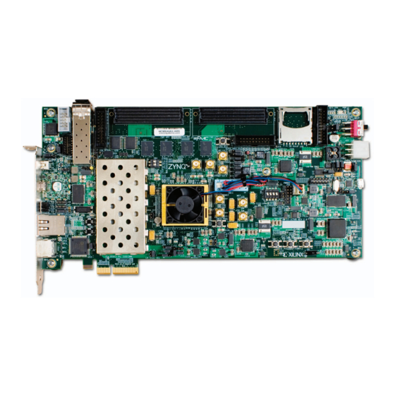
Summary of Contents for Xilinx ZC706
- Page 1 ZC706 Evaluation Board for the Zynq-7000 XC7Z045 All Programmable SoC User Guide UG954 (v1.5) September 10, 2015...
-
Page 2: Revision History
Xilinx’s limited warranty, please refer to Xilinx’s Terms of Sale which can be viewed at www.xilinx.com/legal.htm#tos; IP cores may be subject to warranty and support terms contained in a license issued to you by Xilinx. Xilinx products are not designed or intended to be fail-safe or for use in any application requiring fail-safe performance;... - Page 3 User Pushbuttons, page Table 1-33, J5 pin H22 changed to XC7Z045 (U1) pin AH26 and H23 changed to AH27. The section ZC706 Board Power System, page 72 was added. Voltage levels were changed in VADJ Voltage Control, page Table 1-37...
-
Page 4: Table Of Contents
ZC706 Evaluation Board Features ........ - Page 5 Installing the ZC706 Board in a PC Chassis ....... . .
- Page 6 Markings ............... 115 ZC706 Evaluation Board User Guide www.xilinx.com...
-
Page 7: Chapter 1: Zc706 Evaluation Board Features
ZC706 Evaluation Board Features Overview The ZC706 evaluation board for the XC7Z045 All Programmable SoC (AP SoC) provides a hardware environment for developing and evaluating designs targeting the Zynq®-7000 XC7Z045-2FFG900C AP SoC. The ZC706 evaluation board provides features common to many embedded processing systems, including DDR3 SODIMM and component memory, a four-lane PCI Express®... - Page 8 ° • Status LEDs: Ethernet status ° TI Power Good ° Linear Power Good ° PS DDR3 Component V Good ° PL DDR3 SODIMM V Good ° ZC706 Evaluation Board User Guide www.xilinx.com Send Feedback UG954 (v1.5) September 10, 2015...
- Page 9 • Configuration options: Dual Quad-SPI flash memory ° USB JTAG configuration port (Digilent module) ° Platform cable header JTAG configuration port ° 20-pin PL PJTAG header ° ZC706 Evaluation Board User Guide www.xilinx.com Send Feedback UG954 (v1.5) September 10, 2015...
-
Page 10: Block Diagram
Note: board. The ZC706 evaluation board can be damaged by electrostatic discharge (ESD). Follow ESD CAUTION! prevention measures when handling the board. ZC706 Evaluation Board User Guide www.xilinx.com... - Page 11 Round callout references a component Square callout references a component on the front side of the board on the back side of the board UG954_c1_02_042114 Figure 1-2: ZC706 Evaluation Board Component Locations Table 1-1: ZC706 Evaluation Board Component Descriptions Schematic 0381513 Callout...
- Page 12 Overview Table 1-1: ZC706 Evaluation Board Component Descriptions (Cont’d) Schematic 0381513 Callout Feature Notes Page Number Programmable User Clock, page 35 Silicon Labs SI570BAB0000544DG, default 156.250 MHz C Prog. User Clock 3.3V LVDS (U37, bottom of board) User SMA Clock Source, page 36...
- Page 13 Overview Table 1-1: ZC706 Evaluation Board Component Descriptions (Cont’d) Schematic 0381513 Callout Feature Notes Page Number GPIO DIP Switch, page 60 4-pole C&K SDA04H1SBD GPIO DIP Switch (SW12) ARM® core PJTAG Header (J64) 2x10 0.1inch male header, Samtec TST-110-01-G-D User PMOD GPIO Headers, page 60 2x6 0.1 inch male header...
-
Page 14: Feature Descriptions
[Figure 1-2, callout 1] The ZC706 evaluation board is populated with the Zynq-7000 XC7Z045-2FFG900C AP SoC. The XC7Z045 AP SoC consists of an integrated processing system (PS) and programmable logic (PL), on a single die. The high-level block diagram is shown in Figure 1-3. -
Page 15: Device Configuration
For a secure boot, the PL must be powered on to enable the use of the security block located within the PL, which provides 256-bit AES and SHA decryption/authentication. The ZC706 evaluation board supports these configuration options: • PS Configuration: Quad-SPI flash memory •... -
Page 16: Encryption Key Backup Circuit
For more information about Zynq-7000 AP SoC configuration settings, see Zynq-7000 All Programmable SoC Technical Reference Manual (UG585). Encryption Key Backup Circuit The XC7Z045 AP SoC U1 implements bitstream encryption key technology. The ZC706 board provides the encryption key backup battery circuit shown in Figure 1-5. -
Page 17: I/O Voltage Rails
Figure 1-5: Encryption Key Backup Circuit I/O Voltage Rails There are eleven I/O banks available on the XC7Z045 AP SoC. The voltages applied to the XC7Z045 AP SoC I/O banks used by the ZC706 evaluation board are listed in Table 1-3. -
Page 18: Ddr3 Sodimm Memory (Pl)
1.8V PHY_IF,SDIO_IF,USB_IF PS Bank 502 PS_DDR3_IF Notes: 1. The ZC706 evaluation board is shipped with V set to 2.5V. DDR3 SODIMM Memory (PL) [Figure 1-2, callout 2] The memory module at J1 is a 1 GB DDR3 small outline dual-inline memory module (SODIMM). - Page 19 PL_DDR3_D17 SSTL15 DQ17 PL_DDR3_D18 SSTL15 DQ18 PL_DDR3_D19 SSTL15 DQ19 PL_DDR3_D20 SSTL15 DQ20 PL_DDR3_D21 SSTL15 DQ21 PL_DDR3_D22 SSTL15 DQ22 PL_DDR3_D23 SSTL15 DQ23 PL_DDR3_D24 SSTL15 DQ24 PL_DDR3_D25 SSTL15 DQ25 ZC706 Evaluation Board User Guide www.xilinx.com Send Feedback UG954 (v1.5) September 10, 2015...
- Page 20 PL_DDR3_D52 SSTL15 DQ52 PL_DDR3_D53 SSTL15 DQ53 PL_DDR3_D54 SSTL15 DQ54 PL_DDR3_D55 SSTL15 DQ55 PL_DDR3_D56 SSTL15 DQ56 PL_DDR3_D57 SSTL15 DQ57 PL_DDR3_D58 SSTL15 DQ58 PL_DDR3_D59 SSTL15 DQ59 PL_DDR3_D60 SSTL15 DQ60 ZC706 Evaluation Board User Guide www.xilinx.com Send Feedback UG954 (v1.5) September 10, 2015...
- Page 21 PL_DDR3_DQS7_N DIFF_SSTL15 DQS7_N PL_DDR3_DQS7_P DIFF_SSTL15 DQS7_P PL_DDR3_ODT0 SSTL15 ODT0 PL_DDR3_ODT1 SSTL15 ODT1 PL_DDR3_RESET_B SSTL15 RESET_B PL_DDR3_S0_B SSTL15 S0_B PL_DDR3_S1_B SSTL15 S1_B PL_DDR3_TEMP_EVE SSTL15 EVENT_B PL_DDR3_WE_B SSTL15 WE_B ZC706 Evaluation Board User Guide www.xilinx.com Send Feedback UG954 (v1.5) September 10, 2015...
-
Page 22: Ddr3 Component Memory (Ps)
DIFF_SSTL15 CK1_P The ZC706 DDR3 SODIMM interface adheres to the constraints guidelines documented in the “Dynamic Memory” section of the Zynq-7000 All Programmable SoC PCB Design and Pin Planning Guide (UG933). The ZC706 DDR3 SODIMM interface is a 40Ω impedance implementation. - Page 23 PS_DDR3_DQS0_N DQS0_N PS_DDR3_DM1 PS_DDR3_DQS1_P DQS1_P PS_DDR3_DQS1_N DQS1_N PS_DDR3_DM2 PS_DDR3_DQS2_P DQS2_P PS_DDR3_DQS2_N DQS2_N PS_DDR3_DM3 PS_DDR3_DQS3_P DQS3_P PS_DDR3_DQS3_N DQS3_N PS_DDR3_A0 U2, U3, U4, U5 PS_DDR3_A1 U2, U3, U4, U5 ZC706 Evaluation Board User Guide www.xilinx.com Send Feedback UG954 (v1.5) September 10, 2015...
- Page 24 The ZC706 DDR3 component interface adheres to the constraints guidelines documented in the DDR3 Design Guidelines section of Zynq-7000 All Programmable SoC PCB Design and Pin Planning Guide (UG933). The ZC706 DDR3 component interface is a 40Ω impedance implementation. For more details, see the MT41J256M8HX-15E data sheet [Ref 34].
-
Page 25: Quad-Spi Flash Memory
The configuration section of the Zynq-7000 All Programmable SoC Technical Reference Manual UG585, provides details on using the Quad-SPI flash memory. Figure 1-6 shows the connections of the linear Quad-SPI flash memory on the ZC706 evaluation board. For more details, see the Spansion S25FL128SAGMFIR01 data sheet [Ref 16]. - Page 26 C715 0.1UF 0.1UF R532 R529 R208 R530 1/10W 1/10W S25FL128SAGMFIR01 QSPI1_IO3 QSPI1_CLK DQ3_HOLD_B QSPI1_IO0 QSPI1_CS_B QSPI1_IO1 QSPI1_IO2 DQ2_VPP_WP_B SO16_50P300X413 UG954_c1_06_073013 Figure 1-6: 128 Mb Quad-SPI Flash Memory ZC706 Evaluation Board User Guide www.xilinx.com Send Feedback UG954 (v1.5) September 10, 2015...
-
Page 27: Usb 2.0 Ulpi Transceiver
ULPI Transceiver at U12 to support a USB connection to the host computer. A USB cable is supplied in the ZC706 evaluation kit (Standard-A connector to host computer, Micro-B connector to ZC706 evaluation board connector J2). The USB3320 is a high-speed USB 2.0 PHY supporting the UTMI+ low pin interface (ULPI) interface standard. The ULPI standard defines the interface between the USB controller IP and the PHY device which drives the physical USB bus. - Page 28 For additional information on the Zynq-7000 AP SoC device USB controllers, see Zynq-7000 All Programmable SoC Overview (DS190) and Zynq-7000 All Programmable SoC Technical Reference Manual (UG585). ZC706 Evaluation Board User Guide www.xilinx.com Send Feedback UG954 (v1.5) September 10, 2015...
-
Page 29: Sd Card Interface
[Figure 1-2, callout 5] The ZC706 evaluation board includes a secure digital input/output (SDIO) interface to provide user-logic access to general purpose nonvolatile SDIO memory cards and peripherals. Information for the SD I/O card specification can be found at the SanDisk and... - Page 30 Feature Descriptions Figure 1-8 shows the connections of the SD card interface on the ZC706 evaluation board. X-Ref Target - Figure 1-8 VCCP1V8 VCC3V3_PS 0.1 μF 4.7 KΩ 4.7 KΩ 1/10W 1/10W 67840-8001 SDIO_CD_DAT3 CD_DAT3 SDIO_CMD VSS1 SDIO_CLK VSS2 SDIO_DAT0...
-
Page 31: Programmable Logic Jtag Programming Options
Feature Descriptions Programmable Logic JTAG Programming Options [Figure 1-2, callout 6] The ZC706 evaluation board JTAG chain is shown in Figure 1-9. X-Ref Target - Figure 1-9 SPST Bus Switch SPST Bus Switch JTAG Header N.C. N.C. 3.3V 3.3V FMC HPC... - Page 32 DIP switch SW4 setting 11 selects the JTAG 20-pin header at J62. The four JTAG signals TDI, TDO, TCK, and TMS would be connected to J62 through flying leads from a JTAG cable. The 3-to-1 analog switch settings are shown in Table 1-11. ZC706 Evaluation Board User Guide www.xilinx.com Send Feedback UG954 (v1.5) September 10, 2015...
-
Page 33: Fmc Connector Jtag Bypass
TDI-to-TDO connection through a device or bypass jumper for the JTAG chain to be completed to the AP SoC U1. The JTAG connectivity on the ZC706 board allows a host computer to download bitstreams to the AP SoC using the Xilinx® iMPACT software. In addition, the JTAG connector allows debug tools such as the Vivado serial I/O analyzer or a software debugger to access the SoC. -
Page 34: System Clock
Feature Descriptions Table 1-12: ZC706 Evaluation Board Clock Sources Clock Name Clock Source Description SiT9102 2.5V LVDS 200 MHz fixed-frequency oscillator (SiTime). System Clock System Clock, page Si570 3.3V LVDS I C programmable oscillator, 156.250 MHz default User Clock (Silicon Labs). See... -
Page 35: Programmable User Clock
156.250 MHz. User applications can change the output frequency within the range of 10 MHz to 810 MHz through an I interface. Power cycling the ZC706 evaluation board reverts the user clock to the default frequency of 156.250 MHz. -
Page 36: User Sma Clock Source
[Ref 21]. User SMA Clock Source The ZC706 board provides a pair of SMAs for differential user clock input into PL Bank 9 (see Figure 1-13). The P-side SMA J67 signal USER_SMA_CLOCK_P is connected to U1 pin AD18, with the N-side SMA J68 signal USER_SMA_CLOCK_N connected to U1 pin AD19. Bank 9 Vcco is VADJ_FPGA, a variable voltage (1.8V, 2.5V, 3.3V) depending on the ZC706 FMC... -
Page 37: Processing System Clock Source
[Figure 1-2, callout 10] The ZC706 board includes a pair of SMA connectors for a GTX clock wired to GTX Quad bank 111. This differential clock has signal names SMA_MGT_REFCLK_P and SMA_REFCLK_N, which are connected to AP SoC U1 pins W8 and W7 respectively. -
Page 38: Jitter Attenuated Clock
[Figure 1-2, callout 11] The ZC706 board includes a Silicon Labs Si5324 jitter attenuator U60 on the back side of the board. AP SoC user logic can implement a clock recovery circuit and then output this clock to a differential I/O pair on I/O bank 9 (REC_CLOCK_C_P, AP SoC U1 pin AD20 and REC_CLOCK_C_N, AP SoC U1 pin AE20) for jitter attenuation. -
Page 39: Gtx Transceivers
[Ref 21]. GTX Transceivers [Figure 1-2, callout 12] The ZC706 board provides access to 16 GTX transceivers: • Four of the GTX transceivers are wired to the PCI Express x4 endpoint edge connector (P4) fingers • Eight of the GTX transceivers are wired to the FMC HPC connector (J37) •... - Page 40 The GTX transceivers in Zynq-7000 series AP SoCs are grouped into four channels described as Quads. The reference clock for a Quad can be sourced from the Quad above or Quad below the GTX Quad of interest. There are four GTX Quads on the ZC706 board with connectivity as shown here: •...
- Page 41 MGTPTXP2_109 FMC_HPC_DP2_C2M_P FMC HPC MGTPTXN2_109 FMC_HPC_DP2_C2M_N GTX_BANK_109 MGTPRXP2_109 FMC_HPC_DP2_M2C_P MGTPRXN2_109 FMC_HPC_DP2_M2C_N MGTPTXP3_109 FMC_HPC_DP3_C2M_P MGTPTXN3_109 FMC_HPC_DP3_C2M_N MGTPRXP3_109 FMC_HPC_DP3_M2C_P MGTPRXN3_109 FMC_HPC_DP3_M2C_N AD10 MGTREFCLK0P_109 FMC_HPC_GBTCLK0_M2C_C_P MGTREFCLK0N_109 FMC_HPC_GBTCLK0_M2C_C_N AF10 MGTREFCLK1P_109 MGTREFCLK1N_109 ZC706 Evaluation Board User Guide www.xilinx.com Send Feedback UG954 (v1.5) September 10, 2015...
- Page 42 1. AP SoC U1 GTX input clock nets are capacitively coupled to the FMC HPC J37 pins. 2. AP SoC U1 GTX input clock nets are capacitively coupled to the SI5324C Recovery Clock U60 output pins. ZC706 Evaluation Board User Guide www.xilinx.com Send Feedback UG954 (v1.5) September 10, 2015...
- Page 43 2. AP SoC U1 GTX input nets are capacitively coupled to the RX and MGT_REFCLK SMA pins. For additional information on Zynq-7000 GTX transceivers, see 7 Series FPGAs GTX/GTH Transceivers User Guide (UG476). ZC706 Evaluation Board User Guide www.xilinx.com Send Feedback...
-
Page 44: Pci Express Endpoint Connectivity
85Ω ±10%. The PCIe clock is routed as a 100Ω differential pair. The XC7Z045-2FFG900C AP SoC (-2 speed grade) included with the ZC706 board supports up to Gen2 x4. The PCIe clock is input from the edge connector. It is AC coupled to the AP SoC through the MGTREFCLK0 pins of Quad 112. - Page 45 For additional information about Zynq-7000 PCIe functionality, see 7 Series FPGAs Integrated Block for PCI Express Product Guide for Vivado Design Suite ( ). Additional PG054 information about the PCI Express standard is available [Ref 22]. ZC706 Evaluation Board User Guide www.xilinx.com Send Feedback UG954 (v1.5) September 10, 2015...
-
Page 46: Sfp/Sfp+ Module Connector
Feature Descriptions SFP/SFP+ Module Connector [Figure 1-2, callout 14] The ZC706 board contains a small form-factor pluggable (SFP/SFP+) connector and cage assembly P2 that accepts SFP or SFP+ modules. Figure 1-19 shows the SFP/SFP+ module connector circuitry. X-Ref Target - Figure 1-19... -
Page 47: 10/100/1000 Mb/S Tri-Speed Ethernet Phy (Pl)
[Figure 1-2, callout 15] The ZC706 evaluation board uses the Marvell Alaska PHY device (88E1116R) at U51 for Ethernet communications at 10 Mb/s, 100 Mb/s, or 1000 Mb/s. The board supports RGMII mode only. The PHY connection to a user-provided Ethernet cable is through a Halo HFJ11-1G01E RJ-45 connector (P3) with built-in magnetics. -
Page 48: Ethernet Phy Clock Source
Ethernet PHY Clock Source A 25.00 MHz 50 ppm crystal at X1 is the clock source for the 881116R PHY at U51. Figure 1-20 shows the clock source. ZC706 Evaluation Board User Guide www.xilinx.com Send Feedback UG954 (v1.5) September 10, 2015... -
Page 49: Usb-To-Uart Bridge
ZC706 evaluation kit (Standard-A end to host computer, Type Mini-B end to ZC706 evaluation board connector J21). The CP2103GM is powered by the USB 5V provided by the host PC when the USB cable is plugged into the USB port on the ZC706 evaluation board. -
Page 50: Hdmi Video Output
[Figure 1-2, callout 18] The ZC706 evaluation board provides a high-definition multimedia interface (HDMI®) video output using an Analog Devices ADV7511KSTZ-P HDMI transmitter at U53. The HDMI transmitter U53 is connected to the XC7Z045 AP SoC PL-side banks 12 and 13 and its output is provided on a Molex 500254-1927 HDMI type-A receptacle at P1. - Page 51 GND2 GND3 I2S0 GND4 I2S1 GND5 I2S2 GND6 I2S3 GND7 SCLK GND8 LRCLK GND9 GND10 R_EXT GND11 R158 887Ω 1/10W 1% UG954_c1_21_041113 Figure 1-21: HDMI Codec Circuit ZC706 Evaluation Board User Guide www.xilinx.com Send Feedback UG954 (v1.5) September 10, 2015...
- Page 52 LVCMOS25 HDMI_R_D34 LVCMOS25 AC22 HDMI_R_D35 LVCMOS25 HDMI_R_DE LVCMOS25 HDMI_R_HSYNC LVCMOS25 HSYNC HDMI_R_VSYNC LVCMOS25 VSYNC HDMI_R_CLK LVCMOS25 AC23 HDMI_INT LVCMOS25 AC21 HDMI_R_SPDIF LVCMOS25 SPDIF AB22 HDMI_SPDIF_OUT_LS LVCMOS25 SPDIF_OUT ZC706 Evaluation Board User Guide www.xilinx.com Send Feedback UG954 (v1.5) September 10, 2015...
-
Page 53: I2C Bus
Guide for Vivado Design Suite (PG064). I2C Bus [Figure 1-2, callout 20] The ZC706 evaluation board implements two ports on the XC7Z045 AP SoC. The PL-side port (IIC_SDA and _SCL_MAIN) is routed to level shifter U87. The PS-side port (PS_SDA and _SCL_MAIN) is routed to level shifter U88. The "output" side of the two level... - Page 54 For additional information on the Zynq-7000 AP SoC device I C controller, see Zynq-7000 All Programmable SoC Overview (DS190) and Zynq-7000 All Programmable SoC Technical Reference Manual (UG585). ZC706 Evaluation Board User Guide www.xilinx.com Send Feedback UG954 (v1.5) September 10, 2015...
-
Page 55: Real Time Clock (Rtc)
U65.11 (PCA9548 SC4) IIC_RTC_SDA U65.10 (PCA9548 SD4) IIC_RTC_IRQ_1_B U1.AA17 (XC7Z045 AP SoC PL BANK 10) Information about the RTC-8564JE is available at the Epson Electronics America website [Ref 30]. ZC706 Evaluation Board User Guide www.xilinx.com Send Feedback UG954 (v1.5) September 10, 2015... -
Page 56: Status And User Leds
VCCAUX VCCAUX voltage on indicator DS27 DS28 PHY_LED0 Ethernet PHY LED0 DS29 PHY_LED1 Ethernet PHY LED1 DS30 PHY_LED2 Ethernet PHY LED2 GPIO_LED_0 General Purpose user LED DS35 ZC706 Evaluation Board User Guide www.xilinx.com Send Feedback UG954 (v1.5) September 10, 2015... -
Page 57: Ethernet Phy User Leds
460 mW UG954_c1_24_041113 Figure 1-24: Ethernet PHY User LEDs User I/O [Figure 1-2, callout 22–24] The ZC706 evaluation board provides the following user and general purpose I/O capabilities: • Four user LEDs (callout 22) GPIO_LED_LEFT DS8, GPIO_LED_CENTER DS9, GPIO_LED_RIGHT DS10, °... -
Page 58: User Leds
2 x 6 0.1 in. pitch PMOD2 J58 User LEDs [Figure 1-2, callout 22] The ZC706 evaluation board supports four user LEDs connected to XC7Z045 AP SoC Banks 11, 33, and 35. Figure 1-25 shows the user LED circuits. X-Ref Target - Figure 1-25... -
Page 59: User Pushbuttons
Table 1-29: User Pushbutton Connections to XC7Z045 AP SoC U1 XC7Z045 AP SoC (U1) Pin Net Name I/O Standard Pushbutton Reference AK25 GPIO_SW_LEFT LVCMOS25 GPIO_SW_CENTER LVCMOS25 GPIO_SW_RIGHT LVCMOS25 PL_CPU_RESET LVCMOS15 SW13 ZC706 Evaluation Board User Guide www.xilinx.com Send Feedback UG954 (v1.5) September 10, 2015... -
Page 60: Gpio Dip Switch
[Figure 1-2, callout 26] The ZC706 evaluation board GPIO 2 x 6 male headers J57 and J58 support Digilent Pmod Peripheral Modules. J57 pins (IIC_PMOD_[0:7]) are connected to the TI TCA6416APWR I2C expansion port device U16. J58 pins (PMOD1_[0:7]) are connected to the TI TXS0108E 3.3V-to-VADJ level-shifter U40. - Page 61 VCCA VCCB PMOD1_0_LS PMOD1_0 HDR_2X6 PMOD1_1_LS PMOD1_1 VCC3V3 PMOD1_2_LS PMOD1_2 PMOD1_3_LS PMOD1_3 PMOD1_4_LS PMOD1_4 PMOD1_5_LS PMOD1_5 PMOD1_6_LS PMOD1_6 PMOD1_7_LS PMOD1_7 TSSOP_20 UG954_c1_28_031715 Figure 1-28: User GPIO Headers ZC706 Evaluation Board User Guide www.xilinx.com Send Feedback UG954 (v1.5) September 10, 2015...
-
Page 62: Switches
[Figure 1-2, callout 27] The ZC706 evaluation board power switch is SW1. Sliding the switch actuator from the Off to On position applies 12V power from J22 a 6-pin mini-fit connector. Green LED DS22 illuminates when the ZC706 evaluation board power is on. See Power Management details on the onboard power system. -
Page 63: Program_B Pushbutton
Feature Descriptions Do NOT plug a PC ATX power supply 6-pin connector into J22 on the ZC706 Evaluation CAUTION! Board. The ATX 6-pin connector has a different pinout than J22. Connecting an ATX 6-pin connector into J22 will damage the ZC706 Evaluation Board and void the board warranty. -
Page 64: Ps Power-On And System Reset Pushbuttons
PS_POR_B: This reset is used to hold the PS in reset until all PS power supplies are at the required voltage levels. It must be held Low through PS power-up. PS_POR_B should be generated by the power supply power-good signal. ZC706 Evaluation Board User Guide www.xilinx.com Send Feedback... -
Page 65: Fpga Mezzanine (Fmc) Card Interface
HPC connector is populated with 400 pins, while the LPC connector is partially populated with 160 pins. The connectors are keyed so that a mezzanine card, when installed in either of these FMC connectors on the ZC706 evaluation board, faces away from the ZC706 board. Connector Type: •... - Page 66 FMC_HPC_DP0_C2M_P AK10 PWRCTL1_FMC_PG_C2M LVCMOS25 AB20 FMC_HPC_DP0_C2M_N FMC_HPC_GBTCLK0_M2C_P AD10 FMC_HPC_DP0_M2C_P AH10 FMC_HPC_GBTCLK0_M2C_N FMC_HPC_DP0_M2C_N FMC_HPC_LA01_CC_P LVCMOS25 AG21 FMC_HPC_LA06_P LVCMOS25 AG22 FMC_HPC_LA01_CC_N LVCMOS25 AH21 FMC_HPC_LA06_N LVCMOS25 AH22 FMC_HPC_LA05_P LVCMOS25 AH23 ZC706 Evaluation Board User Guide www.xilinx.com Send Feedback UG954 (v1.5) September 10, 2015...
- Page 67 GA0 = 0 = GND FMC_HPC_LA26_N LVCMOS25 VCC12_P FMC_HPC_TCK_BUF U23.15 VCC12_P FMC_TDI_BUF U23.18 VCC3V3 FMC_HPC_TDO_FMC_LPC_TDI U32.2 VCC3V3 FMC_HPC_TMS_BUF U23.17 GA1 = 0 = GND VCC3V3 VCC3V3 VCC3V3 FMC_HPC_PG_M2C U16.16 ZC706 Evaluation Board User Guide www.xilinx.com Send Feedback UG954 (v1.5) September 10, 2015...
- Page 68 FMC_HPC_LA29_P LVCMOS25 FMC_HPC_LA24_P LVCMOS25 FMC_HPC_LA29_N LVCMOS25 FMC_HPC_LA24_N LVCMOS25 FMC_HPC_LA31_P LVCMOS25 FMC_HPC_LA28_P LVCMOS25 FMC_HPC_LA31_N LVCMOS25 FMC_HPC_LA28_N LVCMOS25 FMC_HPC_LA33_P LVCMOS25 FMC_HPC_LA30_P LVCMOS25 FMC_HPC_LA33_N LVCMOS25 FMC_HPC_LA30_N LVCMOS25 VADJ FMC_HPC_LA32_P LVCMOS25 ZC706 Evaluation Board User Guide www.xilinx.com Send Feedback UG954 (v1.5) September 10, 2015...
-
Page 69: Lpc Connector J5
1. No I/O standards are associated with MGT connections. LPC Connector J5 [Figure 1-2, callout 31] The 160-pin LPC connector defined by the FMC specification (Figure B-1, page 90) provides connectivity for up to: ZC706 Evaluation Board User Guide www.xilinx.com Send Feedback UG954 (v1.5) September 10, 2015... - Page 70 FMC_LPC_LA23_P LVCMOS25 AJ26 FMC_LPC_IIC_SCL U65.15 FMC_LPC_LA23_N LVCMOS25 AK26 FMC_LPC_IIC_SDA U65.14 FMC_LPC_LA26_P LVCMOS25 AJ30 GA0 = 0 = GND FMC_LPC_LA26_N LVCMOS25 AK30 VCC12_P FMC_LPC_TCK_BUF U23.14 VCC12_P FMC_HPC_TDO_FMC_LPC_TDI U31.1 ZC706 Evaluation Board User Guide www.xilinx.com Send Feedback UG954 (v1.5) September 10, 2015...
- Page 71 FMC_LPC_LA33_P LVCMOS25 FMC_LPC_LA30_P LVCMOS25 AB29 FMC_LPC_LA33_N LVCMOS25 AA30 FMC_LPC_LA30_N LVCMOS25 AB30 VADJ FMC_LPC_LA32_P LVCMOS25 FMC_LPC_LA32_N LVCMOS25 VADJ Notes: 1. No I/O standards are associated with MGT connections. ZC706 Evaluation Board User Guide www.xilinx.com Send Feedback UG954 (v1.5) September 10, 2015...
-
Page 72: Zc706 Board Power System
Feature Descriptions ZC706 Board Power System The ZC706 board hosts a power system based on the Texas Instruments (TI) UCD90120A power supply sequencer and monitor, and the LMZ31500 and LMZ31700 family voltage regulators. UCD90120A Description The UCD90120A is a 12-rail PMBus/I C addressable power-supply sequencer and monitor. - Page 73 VADJ_FPGA/VADJ and VCC3V3_FPGA/VCC3V3. Refer to UG954 v1.3 and earlier, and to the schematic for the particular version of the ZC706 board prior to Rev. 2.0. Notes on ZC706 boards prior to Rev. 2.0: 1. VCCINT is implemented utilizing 2xLMZ22008 8A components (U42, U43) in parallel which provides 16A capability.
- Page 74 Notes: 1. Capacitors labeled Cf are bulk filter capacitors. 2. Voltage Sense is connected a point of load. UG954_c1_33_041615 Figure 1-33: ZC706 TI UCD90120A Controller U48 Power System ZC706 Evaluation Board User Guide www.xilinx.com Send Feedback UG954 (v1.5) September 10, 2015...
-
Page 75: Xadc Power System Measurement
Feature Descriptions The LMZ31520, LMZ31506, and LMZ31710 adjustable voltage regulators have their output voltage set through an external resistor. The regulator topology on the ZC706 board permits the TI UCD90120A module to monitor rail voltage and current. Voltage margining at +5% and -5% is also implemented. - Page 76 Expander UG954_c1_34_041113 Figure 1-34: XADC External MUX Block Diagram Table 1-35 which lists the ZC706 XADC power system voltage and current measurement details for the external MUX U6. Table 1-35: XADC Measurements through MUX U6 Isense Op Amp 8-to-1 MUX U6 Meas.
-
Page 77: Power Management
[Figure 1-2, callout 32] The ZC706 board uses power regulators and a PMBus-compliant system controller from Texas Instruments to supply core and auxiliary voltages. The Texas Instruments Fusion Digital Power graphical user interface is used to monitor the voltage and current levels of the board power modules. - Page 78 V33D_CTL1 3.3V @ 0.25A p. 49 UG954_c1_35_031615 Figure 1-35: Onboard Power Regulators The ZC706 evaluation board uses power regulators and PMBus compliant PWM system controllers from Texas Instruments to supply the core and auxiliary voltages listed in Table 1-36. ZC706 Evaluation Board User Guide www.xilinx.com...
-
Page 79: Vadj Voltage Control
5. VCC3V3 3.30V is also sourced from the Vcc3v3_fpga rail 6. Paralleled dual LMZ22008TZ (U42/U43) 8A 0.8V - 6V Adj. Switching Regulators on ZC706 board versions prior to Rev. 2.0 7. LMZ22010TZ (U98 VCCAUX, U15 VCC3V3_FPGA) 10A 0.8 - 6V Adj. Switching Regulators on ZC706 board versions prior to Rev. -
Page 80: Ap Soc Programmable Logic (Pl) Voltage Control
AP SoC Programmable Logic (PL) Voltage Control All PL and PS power rails are enabled by default. When the ZC706 board is powered on, the state of the PL_PWR_ON signal wired to 2-pin header J66 is sampled by the TI UCD90120A controller U48. - Page 81 1. The values defined in these columns are the voltage and current thresholds that cause the regulator to shut down if the value is exceeded. 2. See Table 1-39 for rail turn on dependency details. The ZC706 power system rail turn on timing is not strictly controlled through the Turn On Delay shown in Table 1-37. The Table 1-37 Turn On Delay delay values are applied after the preceding rail has reached 90% of its nominal voltage.
-
Page 82: Cooling Fan
See [Ref 15]. ADJ, The fan turns on when the ZC706 is powered up due to pull-up resistor R369. The SM_FAN_PWM and SM_FAN_TACH signals are wired to XC7Z045 AP SoC U1 pins AB19 and ZC706 Evaluation Board User Guide www.xilinx.com Send Feedback UG954 (v1.5) September 10, 2015... -
Page 83: Xadc Analog-To-Digital Converter
AA19 respectively, enabling the user to implement their own fan speed control IP in the AP SoC PL logic. More information about the power system components used by the ZC706 evaluation board are available from the Texas Instruments digital power website [Ref 32]. - Page 84 Feature Descriptions The ZC706 evaluation board supports both the internal XC7Z045 AP SoC sensor measurements and the external measurement capabilities of the XADC. Internal measurements of the die temperature, VCCINT, VCCAUX, and VCCBRAM are available. Jumper J52 can be used to select either an external voltage reference (VREF) or on-chip voltage reference for the analog-to-digital converter.
- Page 85 Digital I/O. These pins should come from the same bank. These IOs should 19, 20, 17, XADC_GPIO_3, 2, 1, 0 not be shared with other functions because they are required to support three-state operation. ZC706 Evaluation Board User Guide www.xilinx.com Send Feedback UG954 (v1.5) September 10, 2015...
-
Page 86: Appendix A: Default Switch And Jumper Settings
Appendix A Default Switch and Jumper Settings The default switch and jumper settings for the ZC706 evaluation board are provided in this appendix. Switches [Figure 1-2, callout 24] Default switch settings are listed in Table A-1. The locations of the ZC706 jumper headers... -
Page 87: Jumpers
MIO Select Header MIO2 (Note: DIP SW11 pole 1 QSPI0_IO0 = MIO2_SELECT affects this signal) MIO Select Header MIO3 (Note: DIP SW11 pole 2 QSPI0_IO1 = MIO3_SELECT affects this signal) ZC706 Evaluation Board User Guide www.xilinx.com Send Feedback UG954 (v1.5) September 10, 2015... - Page 88 U38 REF3012 VREF Vin Select Header U38 powered by XADC_VCC (U14 1.85V) SPF+ P2 SFP_RS1 BW Select Header LOW BW TX selected SPF+ P2 SFP_RS0 BW Select Header LOW BW RX selected ZC706 Evaluation Board User Guide www.xilinx.com Send Feedback UG954 (v1.5) September 10, 2015...
- Page 89 Jumpers X-Ref Target - Figure A-1 26 28 9 30 UG954_aA_01_042415 Figure A-1: ZC706 Jumper Header Locations ZC706 Evaluation Board User Guide www.xilinx.com Send Feedback UG954 (v1.5) September 10, 2015...
-
Page 90: Appendix B: Vita 57.1 Fmc Connector Pinouts
Figure B-1 shows the pinout of the FPGA mezzanine card (FMC) low pin count (LPC) connector defined by the VITA 57.1 FMC specification. For a description of how the ZC706 evaluation board implements the FMC specification, see FPGA Mezzanine (FMC) Card... - Page 91 LA33_N HB20_P HB21_N 12P0V DP6_C2M_N HB17_N_CC LA32_N HB20_N 3P3V DP5_C2M_P VIO_B_M2C VADJ VADJ 3P3V DP5_C2M_N VIO_B_M2C VADJ VADJ 3P3V RES0 UG954_aB_02_100112 Figure B-2: FMC HPC Connector Pinout ZC706 Evaluation Board User Guide www.xilinx.com Send Feedback UG954 (v1.5) September 10, 2015...
-
Page 92: Zc706 Evaluation Board Xdc Listing
Appendix C Master Constraints File Listing The master Xilinx Design Constraints (XDC) file template for the ZC706 board provides for designs targeting the ZC706 evaluation board. Net names in the constraints listed below correlate with net names on the latest ZC706 evaluation board schematic. Users must identify the appropriate pins and replace the net names with net names in the user RTL. - Page 93 ZC706 Evaluation Board XDC Listing set_property PACKAGE_PIN AD20 [get_ports REC_CLOCK_C_P] set_property IOSTANDARD LVDS_25 [get_ports REC_CLOCK_C_P] set_property PACKAGE_PIN AJ25 [get_ports SI5324_INT_ALMS] set_property IOSTANDARD LVCMOS25 [get_ports SI5324_INT_ALM_LS] set_property PACKAGE_PIN W23 [get_ports SI5324_RST_LS] set_property IOSTANDARD LVCMOS25 [get_ports SI5324_RST_LS] #FMC HPC #CLK set_property PACKAGE_PIN AF22 [get_ports FMC_HPC_CLK0_M2C_N]...
- Page 94 ZC706 Evaluation Board XDC Listing set_property PACKAGE_PIN AD10 [get_ports FMC_HPC_GBTCLK0_M2C_C_P] set_property PACKAGE_PIN AA7 [get_ports FMC_HPC_GBTCLK1_M2C_C_N] set_property PACKAGE_PIN AA8 [get_ports FMC_HPC_GBTCLK1_M2C_C_P] set_property PACKAGE_PIN AG20 [get_ports FMC_HPC_LA00_CC_N] set_property IOSTANDARD LVCMOS25 [get_ports FMC_HPC_LA00_CC_N] set_property PACKAGE_PIN AF20 [get_ports FMC_HPC_LA00_CC_P] set_property IOSTANDARD LVCMOS25 [get_ports FMC_HPC_LA00_CC_P]...
- Page 95 ZC706 Evaluation Board XDC Listing set_property IOSTANDARD LVCMOS25 [get_ports FMC_HPC_LA12_N] set_property PACKAGE_PIN AF23 [get_ports FMC_HPC_LA12_P] set_property IOSTANDARD LVCMOS25 [get_ports FMC_HPC_LA12_P] set_property PACKAGE_PIN AA23 [get_ports FMC_HPC_LA13_N] set_property IOSTANDARD LVCMOS25 [get_ports FMC_HPC_LA13_N] set_property PACKAGE_PIN AA22 [get_ports FMC_HPC_LA13_P] set_property IOSTANDARD LVCMOS25 [get_ports FMC_HPC_LA13_P]...
- Page 96 ZC706 Evaluation Board XDC Listing set_property IOSTANDARD LVCMOS25 [get_ports FMC_HPC_LA25_P] set_property PACKAGE_PIN T28 [get_ports FMC_HPC_LA26_N] set_property IOSTANDARD LVCMOS25 [get_ports FMC_HPC_LA26_N] set_property PACKAGE_PIN R28 [get_ports FMC_HPC_LA26_P] set_property IOSTANDARD LVCMOS25 [get_ports FMC_HPC_LA26_P] set_property PACKAGE_PIN V29 [get_ports FMC_HPC_LA27_N] set_property IOSTANDARD LVCMOS25 [get_ports FMC_HPC_LA27_N]...
- Page 97 ZC706 Evaluation Board XDC Listing set_property PACKAGE_PIN AF13 [get_ports FMC_LPC_LA00_CC_N] set_property IOSTANDARD LVCMOS25 [get_ports FMC_LPC_LA00_CC_N] set_property PACKAGE_PIN AE13 [get_ports FMC_LPC_LA00_CC_P] set_property IOSTANDARD LVCMOS25 [get_ports FMC_LPC_LA00_CC_P] set_property PACKAGE_PIN AG15 [get_ports FMC_LPC_LA01_CC_N] set_property IOSTANDARD LVCMOS25 [get_ports FMC_LPC_LA01_CC_N] set_property PACKAGE_PIN AF15 [get_ports FMC_LPC_LA01_CC_P]...
- Page 98 ZC706 Evaluation Board XDC Listing set_property PACKAGE_PIN AH16 [get_ports FMC_LPC_LA13_N] set_property IOSTANDARD LVCMOS25 [get_ports FMC_LPC_LA13_N] set_property PACKAGE_PIN AH17 [get_ports FMC_LPC_LA13_P] set_property IOSTANDARD LVCMOS25 [get_ports FMC_LPC_LA13_P] set_property PACKAGE_PIN AF17 [get_ports FMC_LPC_LA14_N] set_property IOSTANDARD LVCMOS25 [get_ports FMC_LPC_LA14_N] set_property PACKAGE_PIN AF18 [get_ports FMC_LPC_LA14_P]...
- Page 99 ZC706 Evaluation Board XDC Listing set_property PACKAGE_PIN AJ30 [get_ports FMC_LPC_LA26_P] set_property IOSTANDARD LVCMOS25 [get_ports FMC_LPC_LA26_P] set_property PACKAGE_PIN AJ29 [get_ports FMC_LPC_LA27_N] set_property IOSTANDARD LVCMOS25 [get_ports FMC_LPC_LA27_N] set_property PACKAGE_PIN AJ28 [get_ports FMC_LPC_LA27_P] set_property IOSTANDARD LVCMOS25 [get_ports FMC_LPC_LA27_P] set_property PACKAGE_PIN AE26 [get_ports FMC_LPC_LA28_N]...
- Page 100 ZC706 Evaluation Board XDC Listing set_property PACKAGE_PIN G2 [get_ports GPIO_LED_CENTER] set_property IOSTANDARD LVCMOS15 [get_ports GPIO_LED_CENTER] set_property PACKAGE_PIN Y21 [get_ports GPIO_LED_LEFT] set_property IOSTANDARD LVCMOS25 [get_ports GPIO_LED_LEFT] set_property PACKAGE_PIN W21 [get_ports GPIO_LED_RIGHT] set_property IOSTANDARD LVCMOS25 [get_ports GPIO_LED_RIGHT] #GPIO PMOD1 set_property PACKAGE_PIN AJ21 [get_ports PMOD1_0_LS]...
- Page 101 ZC706 Evaluation Board XDC Listing set_property PACKAGE_PIN AE30 [get_ports HDMI_R_D20] set_property IOSTANDARD LVCMOS25 [get_ports HDMI_R_D20] set_property PACKAGE_PIN Y25 [get_ports HDMI_R_D21] set_property IOSTANDARD LVCMOS25 [get_ports HDMI_R_D21] set_property PACKAGE_PIN AA29 [get_ports HDMI_R_D22] set_property IOSTANDARD LVCMOS25 [get_ports HDMI_R_D22] set_property PACKAGE_PIN AD30 [get_ports HDMI_R_D23]...
- Page 102 ZC706 Evaluation Board XDC Listing set_property PACKAGE_PIN T5 [get_ports PCIE_RX1_N] set_property PACKAGE_PIN T6 [get_ports PCIE_RX1_P] set_property PACKAGE_PIN U3 [get_ports PCIE_RX2_N] set_property PACKAGE_PIN U4 [get_ports PCIE_RX2_P] set_property PACKAGE_PIN V5 [get_ports PCIE_RX3_N] set_property PACKAGE_PIN V6 [get_ports PCIE_RX3_P] set_property PACKAGE_PIN N3 [get_ports PCIE_TX0_N]...
- Page 103 ZC706 Evaluation Board XDC Listing set_property PACKAGE_PIN L1 [get_ports PL_DDR3_D0] set_property IOSTANDARD SSTL15 [get_ports PL_DDR3_D0] set_property PACKAGE_PIN L2 [get_ports PL_DDR3_D1] set_property IOSTANDARD SSTL15 [get_ports PL_DDR3_D1] set_property PACKAGE_PIN K5 [get_ports PL_DDR3_D2] set_property IOSTANDARD SSTL15 [get_ports PL_DDR3_D2] set_property PACKAGE_PIN J4 [get_ports PL_DDR3_D3]...
- Page 104 ZC706 Evaluation Board XDC Listing set_property PACKAGE_PIN B5 [get_ports PL_DDR3_D27] set_property IOSTANDARD SSTL15 [get_ports PL_DDR3_D27] set_property PACKAGE_PIN A3 [get_ports PL_DDR3_D28] set_property IOSTANDARD SSTL15 [get_ports PL_DDR3_D28] set_property PACKAGE_PIN B1 [get_ports PL_DDR3_D29] set_property IOSTANDARD SSTL15 [get_ports PL_DDR3_D29] set_property PACKAGE_PIN C1 [get_ports PL_DDR3_D30]...
- Page 105 ZC706 Evaluation Board XDC Listing set_property PACKAGE_PIN D14 [get_ports PL_DDR3_D54] set_property IOSTANDARD SSTL15 [get_ports PL_DDR3_D54] set_property PACKAGE_PIN B17 [get_ports PL_DDR3_D55] set_property IOSTANDARD SSTL15 [get_ports PL_DDR3_D55] set_property PACKAGE_PIN B12 [get_ports PL_DDR3_D56] set_property IOSTANDARD SSTL15 [get_ports PL_DDR3_D56] set_property PACKAGE_PIN C12 [get_ports PL_DDR3_D57]...
- Page 106 ZC706 Evaluation Board XDC Listing set_property PACKAGE_PIN L8 [get_ports PL_DDR3_DQS4_P] set_property IOSTANDARD DIFF_SSTL15 [get_ports PL_DDR3_DQS4_P] set_property PACKAGE_PIN F12 [get_ports PL_DDR3_DQS5_N] set_property IOSTANDARD DIFF_SSTL15 [get_ports PL_DDR3_DQS5_N] set_property PACKAGE_PIN G12 [get_ports PL_DDR3_DQS5_P] set_property IOSTANDARD DIFF_SSTL15 [get_ports PL_DDR3_DQS5_P] set_property PACKAGE_PIN E17 [get_ports PL_DDR3_DQS6_N]...
- Page 107 ZC706 Evaluation Board XDC Listing #SFP set_property PACKAGE_PIN Y5 [get_ports SFP_RX_N] set_property PACKAGE_PIN Y6 [get_ports SFP_RX_P] set_property PACKAGE_PIN W3 [get_ports SFP_TX_N] set_property PACKAGE_PIN W4 [get_ports SFP_TX_P] set_property PACKAGE_PIN AA18 [get_ports SFP_TX_DISABLE] set_property IOSTANDARD LVCMOS25 [get_ports SFP_TX_DISABLE] #SMA MGT set_property PACKAGE_PIN AB5 [get_ports SMA_MGT_RX_N]...
-
Page 108: Appendix D: Board Setup
6. Plug the ZC706 board into the PCIe connector at this slot and secure its PCIe bracket to the chassis with a screw at the top of the bracket. - Page 109 Installing the ZC706 Board in a PC Chassis 7. The ZC706 board is taller than standard PCIe cards. Ensure that the height of the card is free of obstructions. 8. Connect the ATX power supply to the ZC706 board using the ATX power supply adapter...
-
Page 110: Appendix E: Board Specifications
Appendix E Board Specifications Dimensions Height 5.5 inch (14.0 cm) Length 10.5 inch (26.7 cm) The ZC706 board height exceeds the standard 4.376 inch (11.15 cm) height of a PCI Express Note: card. Environmental Temperature Operating: 0°C to +45°C Storage: –25°C to +60°C... -
Page 111: Appendix F: Additional Resources
Topics include design assistance, advisories, and troubleshooting tips. References The most up to date information related to the ZC706 board, its documentation, and schematics, are available on the following websites. The Xilinx Zynq-7000 All Programmable SoC ZC706 Evaluation Kit product page: www.xilinx.com/zc706... - Page 112 Other documents associated with Xilinx devices, design tools, intellectual property, boards, and kits are available at the Xilinx documentation website at: www.xilinx.com/support/documentation/index Documents associated with other devices used by the ZC706 evaluation board are available at these vendor websites: 16. Spansion Inc.: www.spansion.com...
- Page 113 36. Sourcegate Technologies: www.sourcegate.net. To order the custom Sourcegate cable, contact Aries Ang, aries.ang@sourcegate.net, +65 6483 2878 for price and availability. The Xilinx ATX cable part number 2600304 is manufactured by Sourcegate Technologies Note: and is equivalent to the Sourcegate Technologies part number AZCBL-WH-11009. Sourcegate only manufactures the latest revision, which is currently A4.
-
Page 114: Appendix G: Regulatory And Compliance Information
This product is designed and tested to conform to the European Union directives and standards described in this section. Refer to the Zynq-7000 AP SoC ZC706 Evaluation Kit - Known Issues and Release Notes Master Answer Record concerning the CE requirements for the PC Test Environment: www.xilinx.com/support/answers/51899... -
Page 115: Electromagnetic Compatibility
This product complies with Directive 2002/95/EC on the restriction of hazardous substances (RoHS) in electrical and electronic equipment. This product complies with CE Directives 2006/95/EC, Low Voltage Directive (LVD) and 2004/108/EC, Electromagnetic Compatibility (EMC) Directive. ZC706 Evaluation Board User Guide www.xilinx.com Send Feedback UG954 (v1.5) September 10, 2015...
Need help?
Do you have a question about the ZC706 and is the answer not in the manual?
Questions and answers