Xilinx ZC702 User Manual
Hide thumbs
Also See for ZC702:
- User manual (79 pages) ,
- Getting started manual (52 pages) ,
- Quick start manual (4 pages)

Subscribe to Our Youtube Channel
Related Manuals for Xilinx ZC702


Summary of Contents for Xilinx ZC702
- Page 1 ZC702 Evaluation Board for the Zynq-7000 XC7Z020 All Programmable SoC User Guide UG850 (v1.2) April 4, 2013...
-
Page 2: Revision History
Limited Warranties which can be viewed at http://www.xilinx.com/warranty.htm; IP cores may be subject to warranty and support terms contained in a license issued to you by Xilinx. Xilinx products are not designed or intended to be fail-safe or for use in any application requiring fail-safe performance;... - Page 3 Minor changes were made to the list, and power and ground pin constraints were removed. Appendix D, Board Specifications: This appendix was added to the book. Appendix F, Regulatory and Compliance Information: A link to the ZC702 board master answer record was added. ZC702 Board User Guide www.xilinx.com UG850 (v1.2) April 4, 2013...
-
Page 4: Table Of Contents
Revision History ..............2 Chapter 1: ZC702 Evaluation Board Features Overview . - Page 5 ZC702 Board UCF Listing ........
- Page 6 Markings ............... . 77 ZC702 Board User Guide www.xilinx.com...
-
Page 7: Chapter 1: Zc702 Evaluation Board Features
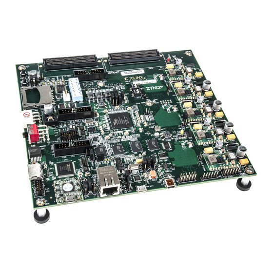
ZC702 Evaluation Board Features Overview The ZC702 evaluation board for the XC7Z020 All Programmable SoC (AP SoC) provides a hardware environment for developing and evaluating designs targeting the Zynq™-7000 XC7Z020-1CLG484C AP SoC. The ZC702 board provides features common to many embedded processing systems, including DDR3 component memory, a tri-mode Ethernet PHY, general purpose I/O, and two UART interfaces. - Page 8 • Power on/off slide switch • Power management with PMBus voltage and current monitoring via TI power controllers • Dual 12-bit 1 MSPS XADC analog-to-digital front end • Configuration options: ZC702 Board User Guide www.xilinx.com UG850 (v1.2) April 4, 2013...
-
Page 9: Block Diagram
Platform cable header JTAG configuration port ° 20-pin PL PJTAG header ° 20-pin PS JTAG header ° Block Diagram The ZC702 board block diagram is shown in Figure 1-1. X-Ref Target - Figure 1-1 Quad SPI JTAG Module DDR3 Memory... -
Page 10: Board Layout
Feature Descriptions starting on page The ZC702 board can be damaged by electrostatic discharge (ESD). Follow ESD prevention CAUTION! measures when handling the board. X-Ref Target - Figure 1-2 Round callout references a component... - Page 11 Overview Note: The image in Figure 1-2 is for reference only and might not reflect the current revision of the board. Table 1-1: ZC702 Board Component Descriptions Schematic Reference 0381449 Callout Component Description Notes Designator Page Number Xilinx part number:...
-
Page 12: Feature Descriptions
[Figure 1-2, callout 1] The ZC702 board is populated with the Zynq-7000 XC7Z020-1CLG484C AP SoC. The XC7Z020 AP SoC consists of an SoC-style integrated processing system (PS) and programmable logic (PL) on a single die. The high-level block diagram is shown in Figure 1-3. - Page 13 USB, Ethernet, SPI, SD/SDIO, I C, CAN, UART, and GPIO. The PS runs independently of the PL and boots at power-up or reset. A system level block diagram is shown in Figure 1-4. ZC702 Board User Guide www.xilinx.com UG850 (v1.2) April 4, 2013...
-
Page 14: Device Configuration
For a secure boot, the PL must be powered on to enable the use of the security block located within the PL, which provides 256-bit AES and SHA decryption/authentication. The ZC702 board supports these configuration options: • PS Configuration: Quad SPI flash memory •... -
Page 15: Encryption Key Backup Circuit
For more information about Zynq-7000 AP SoC configuration settings, see UG585, Zynq-7000 All Programmable SoC Technical Reference Manual. Encryption Key Backup Circuit The XC7Z020 AP SoC U1 implements bitstream encryption key technology. The ZC702 board provides the encryption key backup battery circuit shown in Figure 1-5. -
Page 16: I/O Voltage Rails
Figure 1-5: Encryption Key Backup Circuit I/O Voltage Rails There are four PL I/O banks available on the XC7Z020 AP SoC. The voltages applied to the XC7Z020 AP SoC I/O banks used by the ZC702 board are listed in Table 1-3. -
Page 17: Ddr3 Component Memory
PS_DDR3_DQ10 DQ10 PS_DDR3_DQ11 DQ11 PS_DDR3_DQ12 DQ12 PS_DDR3_DQ13 DQ13 PS_DDR3_DQ14 DQ14 PS_DDR3_DQ15 DQ15 PS_DDR3_DQ16 DQ16 PS_DDR3_DQ17 DQ17 PS_DDR3_DQ18 DQ18 PS_DDR3_DQ19 DQ19 PS_DDR3_DQ20 DQ20 PS_DDR3_DQ21 DQ21 PS_DDR3_DQ22 DQ22 PS_DDR3_DQ23 DQ23 PS_DDR3_DQ24 DQ24 ZC702 Board User Guide www.xilinx.com UG850 (v1.2) April 4, 2013... - Page 18 PS_DDR3_A8 U66, U67, U68, U69 PS_DDR3_A9 U66, U67, U68, U69 PS_DDR3_A10 U66, U67, U68, U69 PS_DDR3_A11 U66, U67, U68, U69 PS_DDR3_A12 U66, U67, U68, U69 PS_DDR3_A13 U66, U67, U68, U69 ZC702 Board User Guide www.xilinx.com UG850 (v1.2) April 4, 2013...
-
Page 19: Quad-Spi Flash Memory
DDR3 Design Guidelines section of 7 Series FPGAs Memory Interface Solutions v1.8 User Guide (UG586). The ZC702 DDR3 memory interface is a 40Ω impedance implementation. Other memory interface details are available in UG586 and 7 Series FPGAs Memory Resources User Guide (UG473). -
Page 20: Usb 2.0 Ulpi Transceiver
The configuration and QSPI section of UG585, Zynq-7000 All Programmable SoC Technical Reference Manual provides details on using the Quad-SPI flash memory. Figure 1-6 shows the connections of the linear Quad-SPI flash memory on the ZC702 board. For more details, see the Numonyx N25Q128A11ESF40G data sheet at the Micron website [Ref... - Page 21 Transceiver at U9 to support a USB connection to the host computer. A USB cable is supplied in the ZC702 Evaluation Kit (Standard-A connector to host computer, Mini-B connector to ZC702 board connector J1). The USB3320 is a high-speed USB 2.0 PHY supporting the UTMI+ low pin interface (ULPI) interface standard. The ULPI standard defines the interface between the USB controller IP and the PHY device which drives the physical USB bus.
- Page 22 USB_CLKOUT PS_MIO31 USB_NXT PS_MIO32 USB_DATA0 PS_MIO33 USB_DATA1 PS_MIO34 USB_DATA2 PS_MIO35 USB_DATA3 PS_MIO28 USB_DATA4 PS_MIO37 USB_DATA5 PS_MIO38 USB_DATA6 PS_MIO39 USB_DATA7 PS_MIO30 USB_STP PS_MIO29 USB_DIR PS_MIO7 USB_RESET_B_AND 27 (via AND gate U62) ZC702 Board User Guide www.xilinx.com UG850 (v1.2) April 4, 2013...
-
Page 23: Sd Card Interface
[Figure 1-2, callout 5] The ZC702 board includes a secure digital input/output (SDIO) interface to provide user-logic access to general purpose non-volatile SDIO memory cards and peripherals. Information for the SD I/O card specification can be found at the SanDisk Corporation... - Page 24 Feature Descriptions Figure 1-8 shows the connections of the SD card interface on the ZC702 board. X-Ref Target - Figure 1-8 VCCMIO_PS VCC3V3 R381 R380 R321 0.1µF 4.7K 4.7K 4.7K 1/10W 1/10W 1/10W 67840-8001 SDIO_CD_DAT3 CD_DAT3 SDIO_CMD VSS1 22 SDIO_CLK...
-
Page 25: Programmable Logic Jtag Programming Options
Feature Descriptions Programmable Logic JTAG Programming Options [Figure 1-2, callout 6] The ZC702 board JTAG chain is shown in Figure 1-9. X-Ref Target - Figure 1-9 SPST Bus Switch SPST Bus Switch JTAG Header N.C. N.C. 3.3V 2.5V FMC LPC... - Page 26 DIP switch SW10 setting 11 selects the JTAG 20-pin header at J58. The four JTAG signals TDI, TDO, TCK, and TMS would be connected to J58 via flying leads from a JTAG cable. The 3-to-1 analog switch settings are shown in Table 1-10. ZC702 Board User Guide www.xilinx.com UG850 (v1.2) April 4, 2013...
-
Page 27: Fmc Connector Jtag Bypass
FMC1_HPC_PRSNT_M2C_B signal. Switch U26 adds an attached FMC to the JTAG chain as determined by the FMC2_LPC_PRSNT_M2C_B signal. Clock Generation The ZC702 board provides three clock sources for the XC7Z020 AP SoC. Table 1-11 lists the source devices for each clock. -
Page 28: System Clock
10 MHz to 810 MHz through an I C interface. Power cycling the ZC702 board reverts the user clock to the default frequency of 156.250 MHz. • Programmable Oscillator: Silicon Labs Si570BAB0000544DG (10 MHz–810 MHz) ZC702 Board User Guide www.xilinx.com... -
Page 29: Processing System Clock Source
Oscillator: SiTime SiT8103AC-23-18E-33.33333 (33.3 MHz) • Frequency jitter: 50 ppm • Single-ended output For more details, see the SiTime SiT8103 data sheet [Ref The system clock circuit is shown in Figure 1-13. ZC702 Board User Guide www.xilinx.com UG850 (v1.2) April 4, 2013... -
Page 30: 10/100/1,000 Mhz Tri-Speed Ethernet Phy
[Figure 1-2, callout 9] The ZC702 board uses the Marvell Alaska PHY device (88E1116R) at U35 for Ethernet communications at 10 Mb/s, 100 Mb/s, or 1,000 Mb/s. The board supports RGMII mode only. The PHY connection to a user-provided Ethernet cable is through a Halo HFJ11-1G01E RJ-45 connector (P2) with built-in magnetics. -
Page 31: Ethernet Phy Clock Source
X-Ref Target - Figure 1-14 C322 18pF 50V 25.00 MHz PHY XTAL OUT R246 C333 PHY XTAL IN 18pF 50V UG850_c1_14_030513 Figure 1-14: Ethernet PHY Clock Source ZC702 Board User Guide www.xilinx.com UG850 (v1.2) April 4, 2013... -
Page 32: Usb-To-Uart Bridge
USB port. The USB cable is supplied in the ZC702 Evaluation Kit (Standard-A end to host computer, Type Mini-B end to ZC702 board connector J17). The CP2103GM is powered by the USB 5V provided by the host PC when the USB cable is plugged into the USB port on the ZC702 board. -
Page 33: Hdmi Video Output
[Figure 1-2, callout 13] The ZC702 board provides a high-definition multimedia interface (HDMI®) video output using an Analog Devices ADV7511KSTZ-P HDMI transmitter at U40. The HDMI output is provided on a Molex 500254-1927 HDMI type-A receptacle at P1. The ADV7511 supports 1080P 60Hz, YCbCr 4:2:2 encoding via 16-bit input data mapping. - Page 34 DSD3 DSD4 DSD5 DSD_CLK MCLK GND1 GND2 GND3 I2S0 GND4 I2S1 GND5 I2S2 GND6 I2S3 GND7 SCLK GND8 LRCLK GND9 GND10 R_EXT GND11 R107 UG850_c1_15_030513 Figure 1-15: HDMI Codec Circuit ZC702 Board User Guide www.xilinx.com UG850 (v1.2) April 4, 2013...
- Page 35 HDMI receptacle P1. Table 1-18: ADV7511 to HDMI Receptacle Connections ADV7511 (U40) Net Name HDMI Receptacle P1 Pin HDMI_D0_P HDMI_D0_N HDMI_D1_P HDMI_D1_N HDMI_D2_P HDMI_D2_N ZC702 Board User Guide www.xilinx.com UG850 (v1.2) April 4, 2013...
-
Page 36: I2C Bus
I2C Bus [Figure 1-2, callout 14] The ZC702 board implements a single I C port on the XC7Z020 AP SoC (IIC_SDA_MAIN, IIC_SDA_SCL), which is routed through an TI Semiconductor PCA9548 1-to-8 channel I bus switch (U44). The bus switch can operate at speeds up to 400 kHz. -
Page 37: Real Time Clock
Clock counter, alarm and fixed-cycle timer interrupt functions Programming information for the RTC-8564JE is available in the RTC-8564JE/NB Application Manual at the Epson Electronics America website [Ref Figure 1-17 shows the real time clock circuit. ZC702 Board User Guide www.xilinx.com UG850 (v1.2) April 4, 2013... -
Page 38: I/O Expansion Header
(IIC_PMOD[0:7]) are connected to the TI TCA6416APWR I C expansion port device U80. See the Digilent website for information on Digilent Pmod Peripheral Modules [Ref 10]. The expansion header circuit is shown in Figure 1-18. ZC702 Board User Guide www.xilinx.com UG850 (v1.2) April 4, 2013... -
Page 39: High Speed Can Transceiver
It supports the differential bus signal representation described in the international standard for in-vehicle high speed CAN applications (ISO 11898). Figure 1-19 shows the controller area network (CAN) bus interface. ZC702 Board User Guide www.xilinx.com UG850 (v1.2) April 4, 2013... - Page 40 Table 1-21: CAN Transceiver AP SoC Connections TJA1040 (U14) TXS0104E Level Shifter (U3) XC7Z020 AP SoC (U1) Net Name Net Name Low Side Net Bank CAN_TXD CAN_TXD_LS PS_MIO47 CAN_RXD CAN_RXD_LS PS_MIO46 CAN_STB_B CAN_STB_B_LS PS_MIO9 ZC702 Board User Guide www.xilinx.com UG850 (v1.2) April 4, 2013...
-
Page 41: Status Leds
Ethernet PHY user LEDs. They are referred in the data sheet as LED0, LED1, and LED2. The data sheet and other product information for the Marvell 88E1116R Alaska Gigabit Ethernet Transceiver is available at the Marvell website [Ref ZC702 Board User Guide www.xilinx.com UG850 (v1.2) April 4, 2013... -
Page 42: User I/O
UG850_c1_20_030513 Figure 1-20: Ethernet PHY User LEDs User I/O [Figure 1-2, callout 17–28] The ZC702 board provides the following user and general purpose I/O capabilities: • Ten user LEDs (callout 17) PMOD0 0–PMOD0 3 and PMOD1 0–PMOD1 3: DS15–DS22 °... -
Page 43: User Leds
[Figure 1-2, callout 17] The ZC702 board supports eight user LEDs connected to XC7Z020 AP SoC Banks 13, 33, 34, and 35 via level-shifters. Note that the LEDs are wired in parallel with headers J63 (PMOD1) and J62 (PMOD2). These headers are described in... - Page 44 460 mW 460 mW 460 mW VCC3V3 VCC3V3 DS23 DS12 VCCMIO (1.8V) R416 R393 20.5K 0.1W 0.1W 0.1W NDS331N NDS331N PS_LED1 PS_MIO8_LED0 460 mW 460 mW UG850_c1_21_030513 Figure 1-21: User LEDs ZC702 Board User Guide www.xilinx.com UG850 (v1.2) April 4, 2013...
-
Page 45: User Pushbuttons
XC7Z020 AP SoC U1. Table 1-24: User Pushbutton Connections to XC7Z020 AP SoC U1 XC7Z020 AP SoC (U1) Pin Net Name Pushbutton and Pin Reference GPIO_SW_N SW5.3 (Left switch) GPIO_SW_S SW7.3 (Right switch) ZC702 Board User Guide www.xilinx.com UG850 (v1.2) April 4, 2013... -
Page 46: Gpio Dip Switch
XC7Z020 AP SoC (U1) Net Name DIP Switch SW12 Pin GPIO_DIP_SW0 GPIO_DIP_SW1 User PS Switches [Figure 1-2, near callout 18] Figure 1-25 shows the user PS pushbutton and DIP switch circuit. ZC702 Board User Guide www.xilinx.com UG850 (v1.2) April 4, 2013... -
Page 47: User Pmod Gpio Headers
SW14.4 and SW15.2 User PMOD GPIO Headers [Figure 1-2, callout 28] The ZC702 board supports two GPIO headers J62 and J63. The PMOD nets connected to these headers are dual-purpose, with the User LEDs, page 43 wired in parallel to the header pins. -
Page 48: Switches
[Figure 1-2, callout 20] The ZC702 board power switch is SW11. Sliding the switch actuator from the Off to On position applies 12V power from J60, a 6-pin mini-fit connector. Green LED DS14 illuminates when the ZC702 board power is on. See... -
Page 49: Program_B Pushbutton
Feature Descriptions Do NOT plug a PC ATX power supply 6-pin connector into J60 on the ZC702 board. The ATX CAUTION! 6-pin connector has a different pinout than J60. Connecting an ATX 6-pin connector into J60 will damage the ZC702 board and void the board warranty. -
Page 50: Ps Power-On And System Reset Pushbuttons
It must be held Low through PS power-up. PS_POR_B should be generated by the power supply power-good signal. Depressing and then releasing pushbutton SW2 causes PS_SRST_B_SW to strobe low. ZC702 Board User Guide www.xilinx.com UG850 (v1.2) April 4, 2013... -
Page 51: Fpga Mezzanine (Fmc) Card Interface
(LPC) connectors at J3 and J4. Both connectors use a 10 x 40 form factor that is partially populated with 160 pins. The connectors are keyed so that a the mezzanine card faces away from the ZC702 board when connected. - Page 52 FMC1_LPC_LA05_P FMC1_LPC_LA10_P FMC1_LPC_LA05_N FMC1_LPC_LA10_N FMC1_LPC_LA09_P FMC1_LPC_LA14_P FMC1_LPC_LA09_N FMC1_LPC_LA14_N FMC1_LPC_LA13_P FMC1_LPC_LA18_CC_P FMC1_LPC_LA13_N FMC1_LPC_LA18_CC_N FMC1_LPC_LA17_CC_P FMC1_LPC_LA27_P FMC1_LPC_LA17_CC_N FMC1_LPC_LA27_N FMC1_LPC_LA23_P FMC1_LPC_IIC_SCL FMC1_LPC_LA23_N FMC1_LPC_IIC_SDA FMC1_LPC_LA26_P FMC1_LPC_LA26_N VCC12_P FMC1_LPC_TCK_BUF VCC12_P FMC_TDI_BUF VCC3V3 FMC1_LPC_TDO_FMC2_LPC_TDI VCC3V3 FMC1_LPC_TMS_BUF ZC702 Board User Guide www.xilinx.com UG850 (v1.2) April 4, 2013...
- Page 53 FMC1_LPC_LA16_N FMC1_LPC_LA11_N FMC1_LPC_LA20_P FMC1_LPC_LA15_P FMC1_LPC_LA20_N FMC1_LPC_LA15_N FMC1_LPC_LA22_P FMC1_LPC_LA19_P FMC1_LPC_LA22_N FMC1_LPC_LA19_N FMC1_LPC_LA25_P FMC1_LPC_LA21_P FMC1_LPC_LA25_N FMC1_LPC_LA21_N FMC1_LPC_LA29_P FMC1_LPC_LA24_P FMC1_LPC_LA29_N FMC1_LPC_LA24_N FMC1_LPC_LA31_P FMC1_LPC_LA28_P FMC1_LPC_LA31_N FMC1_LPC_LA28_N FMC1_LPC_LA33_P FMC1_LPC_LA30_P FMC1_LPC_LA33_N FMC1_LPC_LA30_N VADJ FMC1_LPC_LA32_P FMC1_LPC_LA32_N VADJ ZC702 Board User Guide www.xilinx.com UG850 (v1.2) April 4, 2013...
- Page 54 FMC2_LPC_LA27_N FMC2_LPC_LA23_P FMC2_LPC_IIC_SCL FMC2_LPC_LA23_N FMC2_LPC_IIC_SDA FMC2_LPC_LA26_P FMC2_LPC_LA26_N VCC12_P FMC2_LPC_TCK_BUF VCC12_P FMC1_LPC_TDO_FMC2_LPC_TDI VCC3V3 FMC2_LPC_TDO_FPGA_TDI VCC3V3 FMC2_LPC_TMS_BUF VCC3V3 VCC3V3 VCC3V3 FMC2_LPC_CLK1_M2C_P FMC2_LPC_CLK1_M2C_N FMC2_LPC_PRSNT_M2C_B FMC2_LPC_LA00_CC_P FMC2_LPC_CLK0_M2C_P FMC2_LPC_LA00_CC_N AA19 FMC2_LPC_CLK0_M2C_N AA18 FMC2_LPC_LA03_P AA16 FMC2_LPC_LA02_P ZC702 Board User Guide www.xilinx.com UG850 (v1.2) April 4, 2013...
-
Page 55: Power Management
1-2, callout 25] TheZC702 PCB layout and power system design meets the recommended criteria described in Zynq-7000 All Programmable SoC PCB Design and Pin Planning Guide (UG933). The ZC702 board power distribution diagram is shown in Figure 1-29. ZC702 Board User Guide www.xilinx.com... - Page 56 0.75V at 3A VREF UG850_c1_29_030513 Figure 1-29: Onboard Power Regulators The ZC702 board uses power regulators and a PMBus compliant system controller from Texas Instruments to supply core and auxiliary voltages as listed in Table 1-30. The Texas Instruments Fusion Digital Power graphical user interface is used to monitor the voltage and current levels of the board power modules.
-
Page 57: Vadj Voltage Control
0.75V VADJ Voltage Control The VADJ rail is set to 2.5V. When the ZC702 board is powered on, the state of the FMC_VADJ_ON_B signal wired to header J12 is sampled by the TI UCD9248 controller U33. If a jumper is installed on J12 signal FMC_VADJ_ON_B is held low, and the TI controller U33 energizes the VADJ rail at power on. -
Page 58: Monitoring Voltage And Current
VADJ rail comes up at FMC_VADJ_ON_B the new VADJ voltage level. Installing a jumper at J12 after a ZC702 board powers up in this mode turns on the VADJ rail. - Page 59 1. The values defined in these columns are the voltage, current, and temperature thresholds that causes the regulator to shut down if the value is exceeded. Table 1-33 defines the voltage and current values for each power rail controlled by the UCD9248 PMBus controller at address 54 (U34). ZC702 Board User Guide www.xilinx.com UG850 (v1.2) April 4, 2013...
-
Page 60: Cooling Fan
1-30. X-Ref Target - Figure 1-30 VCC12_P UG850_c1_30_030513 Figure 1-30: Cooling Fan Circuit More information about the power system components used by the ZC702 board are available from the Texas Instruments digital power website [Ref 12]. XADC Analog-to-Digital Converter [Figure 1-2, callout 26] The XC7Z020 AP SoC provides an Analog Front End XADC block. - Page 61 100Ω UG850_c1_31_030513 Figure 1-31: XADC Block Diagram The ZC702 board supports both the internal XC7Z020 AP SoC sensor measurements and the external measurement capabilities of the XADC. Internal measurements of the die temperature, VCCINT, VCCAUX, and VCCBRAM are available. Jumper J37 can be used to select either an external voltage reference (VREF) or on-chip voltage reference for the analog-to-digital converter.
- Page 62 Digital I/O. These pins should come from the same bank. These IOs should XADC_GPIO_3, 2, 1, 0 19, 20, 17, 18 not be shared with other functions because they are required to support three-state operation. ZC702 Board User Guide www.xilinx.com UG850 (v1.2) April 4, 2013...
-
Page 63: Appendix A: Default Switch And Jumper Settings
Right Jumpers [Figure 1-2, callout 24] Default jumper positions are listed in Table A-2. Table A-2: Default Jumper Settings Jumper Function Default Position HDR_1 X 2 CFGBVS short to GND ZC702 Board User Guide www.xilinx.com UG850 (v1.2) April 4, 2013... - Page 64 ETHERNET PHY HDR NONE USB 2.0 MODE USB 2.0 J1 ID SEL USB 2.0 J1 VBUS CAP SEL USB 2.0 J1 GND SEL XADC_VREP SEL XADC_VCC SEL XADC_VREF SOURCE SEL ZC702 Board User Guide www.xilinx.com UG850 (v1.2) April 4, 2013...
-
Page 65: Appendix B: Vita 57.1 Fmc Connector Pinouts
Figure B-1 shows the pinout of the FPGA mezzanine card (FMC) low pin count (LPC) connector defined by the VITA 57.1 FMC specification. For a description of how the ZC702 board implements the FMC specification, see FPGA Mezzanine (FMC) Card Interface,... -
Page 66: Appendix C: Master Ucf Listing
FMC bank I/O standards must be uniquely defined by each customer. Note: The UCF file listed in this appendix might not be the latest version. Always refer to the ZC702 Evaluation Kit product page (www.xilinx.com/products/boards-and-kits/EK-Z7-ZC702-G.htm) for the latest FPGA pins constraints file. - Page 67 ZC702 Board UCF Listing PL_PJTAG_TMS LOC = V9 | IOSTANDARD=LVCMOS25; # Bank 13 VCCO - VADJ - IO_L1N_T0_13 PL_PJTAG_TDI LOC = V8 | IOSTANDARD=LVCMOS25; # Bank 13 VCCO - VADJ - IO_L2P_T0_13 IIC_SDA_MAIN_LS LOC = W8 | IOSTANDARD=LVCMOS25; # Bank 13...
- Page 68 ZC702 Board UCF Listing FMC2_LPC_LA05_N LOC = AB20 | IOSTANDARD=LVCMOS25; # Bank 33 VCCO - VADJ - IO_L10N_T1_33 FMC2_LPC_LA00_CC_P LOC = Y19 | IOSTANDARD=LVCMOS25; # Bank 33 VCCO - VADJ - IO_L11P_T1_SRCC_33 FMC2_LPC_LA00_CC_N LOC = AA19 | IOSTANDARD=LVCMOS25; # Bank 33...
- Page 69 ZC702 Board UCF Listing FMC1_LPC_LA16_N LOC = P15 | IOSTANDARD=LVCMOS25; # Bank 34 VCCO - VADJ - IO_L19N_T3_VREF_34 PMOD2_3_LS LOC = P17 | IOSTANDARD=LVCMOS25; # Bank 34 VCCO - VADJ - IO_L20P_T3_34 PMOD2_2_LS LOC = P18 | IOSTANDARD=LVCMOS25; # Bank 34...
- Page 70 ZC702 Board UCF Listing #NET PHY_TX_CTRL LOC = F11 ; # Bank 501 - PS_MIO21_501 #NET PHY_RXD0 LOC = E11 ; # Bank 501 - PS_MIO23_501 #NET PHY_RXD2 LOC = F12 ; # Bank 501 - PS_MIO25_501 #NET PHY_RX_CTRL LOC = D7 ;...
- Page 71 ZC702 Board UCF Listing #NET PS_DDR3_DM1 LOC = H3 ; # Bank 502 - PS_DDR_DM1_502 #NET PS_DDR3_DQS1_P LOC = H2 ; # Bank 502 - PS_DDR_DQS_P1_502 #NET PS_DDR3_DQS1_N LOC = J2 ; # Bank 502 - PS_DDR_DQS_N1_502 #NET PS_DDR3_DQ12 LOC = L3 ;...
-
Page 72: Appendix D: Board Specifications
Dimensions Width: 7.750 in. (19.685 cm) Length: 7.150 in. (18.161 cm) Environmental Temperature Operating: 0°C to +45°C Storage: –25°C to +60°C Humidity 10% to 90% non-condensing Operating Voltage +12 V ZC702 Board User Guide www.xilinx.com UG850 (v1.2) April 4, 2013... -
Page 73: Appendix E: Additional Resources
Topics include design assistance, advisories, and troubleshooting tips. Further Resources The most up to date information related to the ZC702 board and its documentation is available on the following websites. The Xilinx Zynq-7000 AP SoC ZC702 Evaluation Kit product page: www.xilinx.com/products/boards-and-kits/EK-Z7-ZC702-G.htm... -
Page 74: References
References These Xilinx documents provide supplemental material useful with this guide: DS190, Zynq-7000 All Programmable SoC Overview DS187, Zynq-7000 All Programmable SoC (XC7Z010 and XC7Z020): DC and AC Switching Characteristics UG138, LogiCORE IP Tri-Mode Ethernet MAC v4.5 User Guide UG470, 7 Series FPGAs Configuration User Guide... - Page 75 11. NXP Semiconductors: ics.nxp.com (TJA01040) 12. Texas Instruments: www.ti.com, www.ti.com/fusiondocs, and www.ti.com/ww/en/analog/digital-power/index.html (UCD9248PFC, PTD08A010W, PTD08A020W, PTD08D210W, LMZ12002, TL1962ADC, TPS51200DR, PCA9548) 13. Samtec: www.samtec.com. (SEAF series connectors) 14. Integrated Device Technology: www.idt.com (ICS844021I) ZC702 Board User Guide www.xilinx.com UG850 (v1.2) April 4, 2013...
-
Page 76: Appendix F: Regulatory And Compliance Information
Regulatory and Compliance Information This product is designed and tested to conform to the European Union directives and standards described in this section. Refer to the ZC702 board master answer record concerning the CE requirements for the PC Test Environment: www.xilinx.com/support/answers/47864.htm... - Page 77 This product complies with Directive 2002/95/EC on the restriction of hazardous substances (RoHS) in electrical and electronic equipment. This product complies with CE Directives 2006/95/EC, Low Voltage Directive (LVD) and 2004/108/EC, Electromagnetic Compatibility (EMC) Directive. ZC702 Board User Guide www.xilinx.com UG850 (v1.2) April 4, 2013...
Need help?
Do you have a question about the ZC702 and is the answer not in the manual?
Questions and answers