Table of Contents
Advertisement
Quick Links
Product Family:
DL405
Manual Number
D4-ANLG-M
Revision and Date
5th Ed., Rev. A; July 2004
Changes to Chapter 3: F4–04AD 4-Channel Analog Input
Page 3-3. Module Specifications; General Specifications
In the table, change the Power Budget Requirement value from "85 mA (power from base)" to "150 mA (power from base)".
Page 3-11. Current Loop Transmitter Impedance
Replace the example drawing with this one. Connections were added between the power supply 0V terminal, the 0V CH1
terminal, and the CH1 common terminal. Also, the "See NOTE 3 below" note was added.
R = Tr – Mr
R = 750 – 250
R
500
DC Supply
+36V
0V
Errata Sheet
This Errata Sheet contains corrections or changes
made after the publication of this manual.
R – resistor to add
Tr – Transmitter Requirement
Mr – Module resistance (internal 250 ohms)
Two-wire Transmitter
+
NOTE 3: When a differential input is not used, 0V should
be connected to C of the channel.
Page 1 of 5
Date:
–
R
See NOTE 3 below
September 12, 2018
Module Channel 1
V
C
I
0V
250 ohms
Advertisement
Table of Contents

Related Manuals for Automation Direct DL405

Summary of Contents for Automation Direct DL405
- Page 1 This Errata Sheet contains corrections or changes made after the publication of this manual. Date: September 12, 2018 Product Family: DL405 Manual Number D4-ANLG-M Revision and Date 5th Ed., Rev. A; July 2004 Changes to Chapter 3: F4–04AD 4-Channel Analog Input Page 3-3.
- Page 2 Errata Sheet Changes to Chapter 4: F4-04ADS 4-Channel Isolated Analog Input Page 4-3. Module Specifications; General Specifications In the table, change the Power Budget Requirement value from “270 mA at 5 VDC (from base)” to “370 mA at 5 VDC (from base).”...
- Page 3 Errata Sheet Changes to Chapter 6: F4–16AD-1 16-Channel Analog Input Page 6-4. Setting the Module Jumpers Changes to Chapter 7: F4–16AD-2 16-Channel Analog Input Page 7-4. Setting the Module Jumpers For both modules, the jumpers are now arranged differently. They are no longer in a straight line like the drawings on pages 6-4 and 7-4 show.
- Page 4 Errata Sheet Changes to Chapter 9: F4-08RTD 8-Channel RTD Input Page 9-7. Connecting the Field Wiring; RTD - Resistance Temperature Detector; Lead Detection for RTD Sensors Replace the wiring diagram with this one. The wire lead colors changed. (The two black leads changed to red and the two red leads changed to white.) To CH-- To COM...
- Page 5 Errata Sheet Changes to Chapter 18: F4-04DAS-2 4-Channel Isolated 0–5V, 0–10V Output (continued) Page 18-5. Wiring Diagram In 2008 the module was redesigned and the range selection jumpers on the back of the module were eliminated. The range selection is now done by a wire jumper for each channel located on the terminal block. This wiring diagram was revised to show these jumpers.
- Page 6 DL405 Analog I/O Modules D4–ANLG–M...
- Page 7 WARNING Thank you for purchasing automation equipment from Automationdirect.com, doing business as AutomationDirect. We want your new automation equipment to operate safely. Anyone who installs or uses this equipment should read this publication (and any other relevant publications) before installing or operating the equipment.
- Page 8 AVERTISSEMENT Nous vous remercions d’avoir acheté l’équipement d’automatisation de Automationdirect.com en faisant des affaires comme AutomationDirect. Nous tenons à ce que votre nouvel équipement d’automatisation fonctionne en toute sécurité. Toute personne qui installe ou utilise cet équipement doit lire la présente publication (et toutes les autres publications pertinentes) avant de l’installer ou de l’utiliser.
-
Page 9: Table Of Contents
Table of Contents Chapter 1: Getting Started Introduction ............... . . 1–2 The Purpose of this Manual . - Page 10 Table of Contents Analog Input Modules ............. 1–7 Special Input Modules .
- Page 11 Table of Contents Module Operation ..............3–12 DL430 Special Requirements .
- Page 12 Table of Contents Chapter 4: F4-04ADS 4-Channel Isolated Analog Input Module Specifications ............. . . 4–2 Analog Input Configuration Requirements .
- Page 13 Table of Contents Current Loop Transmitter Impedance ..........5–7 Removable Connector .
- Page 14 Table of Contents Scaling the Input Data ............. 6–16 Analog and Digital Value Conversions .
- Page 15 Table of Contents Connecting the Field Wiring ............8–6 Wiring Guidelines .
- Page 16 viii Table of Contents Writing the Control Program ............9–12 Multiple Active Channels .
- Page 17 Table of Contents Module Resolution 15-Bit Plus Sign (Bipolar Voltage Input) ......10–19 Analog and Digital Value Conversions .
- Page 18 Table of Contents Writing the Control Program ............12–12 Update Any Channel .
- Page 19 Table of Contents Chapter 14: F4–04DA–2 4-Channel Analog Voltage Output Module Specifications ............. . . 14–2 Analog Output Configuration Requirements .
- Page 20 Table of Contents Chapter 15: F4–08DA–1 8-Channel Analog Current Output Module Specifications ............. . . 15–2 Analog Output Configuration Requirements .
- Page 21 xiii Table of Contents Channel Scanning Sequence ............16–7 Output Bit Assignments .
- Page 22 Table of Contents Chapter 18: F4–04DAS–2 4-Channel Isolated Volt Output Module Specifications ............. . . 18–2 Analog Output Configuration Requirements .
- Page 23 Table of Contents Channel Scanning Sequence ............19–7 Output Bit Assignments .
- Page 24 ..........20–28 Appendix A: DL405 Discrete I/O Memory Map X Input / Y Output Bit Map .
- Page 25 Manual Revisions If you contact us in reference to this manual, be sure to include the edition or revision number. Title: DL405 Analog I/O Manual Manual Number: D4–ANLG–M Edition/Rev Date Description of Changes Original 1/94 original issue 2nd Edition 7/95...
- Page 26 Getting Started In This Chapter..Introduction Conventions Used Physical Characteristics Analog Input Module Terminology Analog Output Module Terminology Selecting the Appropriate Module Frequently Asked Questions Analog Made Easy - Four Simple Steps...
-
Page 27: Introduction
I/O points are assigned to the module. Now, you have the material necessary to quickly understand the DL405 Analog I/O modules. So, let’s get started! Technical Support We realize that even though we strive to be the best, we may have arranged our information in such a way you cannot find what you are looking for. -
Page 28: Conventions Used
1–3 Getting Started Conventions Used When you see the “notepad” icon in the left-hand margin, the paragraph to its immediate right will be a special note. The word NOTE: in boldface will mark the beginning of the text. When you see the “exclamation mark” icon in the left-hand margin, the paragraph to its immediate right will be a warning. -
Page 29: Analog Input Module Terminology
1–4 Getting Started Analog Input Module Terminology We use several different terms throughout the rest of this manual. You do not have to be an expert on analog terms to use the products, but it may help make it easier to select the appropriate modules if you take a few minutes to review these definitions. -
Page 30: Analog Output Module Terminology
1–5 Getting Started Analog Output Module Terminology Channels per The total number of analog signals the module sends to field devices. Module Output Ranges The minimum to maximum spans in voltage or current the module outputs, converted from digital values. Resolution The number of binary weighted bits available on the digital side of the module for use in converting the digital value to an analog signal. -
Page 31: Selecting The Appropriate Module
Getting Started Selecting the Appropriate Module Wide Variety of There are a wide variety of Analog I/O modules available for use with the DL405 Modules family of automation products. These modules are well suited for monitoring and controlling various types of analog signals such as pressure, temperature, and so forth. -
Page 32: Analog Input Modules
1–7 Getting Started The following tables provide a condensed version of the information you need to select the appropriate module. The most important thing is to simply determine the number of channels required and the signal ranges that must be supported. Once you’ve determined these parameters, look in the specific chapter for the selected module to determine the installation and operation requirements. -
Page 33: Special Input Modules
1–8 Getting Started Special Input Specification F4–08THM–n F4–08RTD Modules Channels Input Ranges Type E: –270/1000_C (–450/1832_F) Pt100Ω: –200.0/850.0_C Type J: –210/760_C (–350/1390_F) (–328/ 562_F) Type K: –270/1370_C (–450/2500_F) Pt1000Ω: –200.0/595.0_C Type R: 0/1768_C (–32/3214_F) (–328/1103_F) Type S: 0/1768_C (–32/3214_F) jPt100Ω: –38.0/450.0_C Type T: –270/400_C (–450/752_F) (–36/842_F) -
Page 34: Analog Output Modules
1–9 Getting Started Analog Output Specification D4–02DA F4–04DA F4–04DA–1 Modules Channels Output Ranges 4–20 mA, 1–5V, 0–10V 4–20 mA, 0–5V, 4–20mA 0–10V, $5V, $10V Resolution 12 bit (1 in 4096) 12 bit (1 in 4096) 12 bit (1 in 4096) Output Type Independent Single ended... -
Page 35: Physical Characteristics
Q. Does my module detect a broken transmitter or loose terminal block? A. Yes, most of the analog modules have this function. The loose terminal block is indicated by the error code E201. See error code information in the DL405 User Manual for further information. -
Page 36: Analog Made Easy - Four Simple Steps
1–11 Getting Started Analog Made Easy – Four Simple Steps Once you’ve selected the appropriate module, use the chapter that describes the module and complete the following steps. Step 1 . Take a minute to review the detailed specifications to make sure the module meets your application requirements. -
Page 37: Chapter 2: Installation And Wiring
Installation and Wiring In This Chapter..Safety Guidelines I/O Wiring Strategies I/O Module Placement and Wiring... -
Page 38: Safety Guidelines
2–2 Installation and Wiring Safety Guidelines WARNING: Providing a safe operating environment for personnel and equipment is your responsibility and should be your primary goal during system planning and installation. Automation systems can fail and may result in situations that can cause serious injury to personnel or damage to equipment. -
Page 39: Orderly System Shutdown
2–3 Installation and Wiring Orderly System The PLC control program can provide Shutdown the first level of protection when used to identify machine problems. After analyzing your application, identify any shutdown sequences that must be performed. Typical problems include part jams, empty bins, etc. that do not pose a risk of personal injury or equipment damage. -
Page 40: I/O Wiring Strategies
Installation and Wiring I/O Wiring Strategies The DL405 PLC system is very flexible and will work in many different wiring configurations. By studying this section before actual installation, you can probably find the best wiring strategy for your application. This will help to lower system cost, reduce wiring errors, and avoid safety problems. -
Page 41: I/O Module Placement And Wiring
2–5 Installation and Wiring The next figure shows the physical layout of a DL405 PLC system as viewed from the front. In addition to the basic circuits, AC-powered CPUs include an auxiliary +24VDC power supply with its own isolation boundary. Since the supply output is isolated from the other three circuits, it can power input and/or output circuits. -
Page 42: I/O Module Status Indicators
The actual status indicators vary from one module to another, and some modules do not have status indicators. Status indicators Color Coding The DL405 family of I/O modules have a 110VAV INPUT of I/O Modules color-coded stripe on the front bezel to help identify whether the module type is input, output, or special module. -
Page 43: Wiring A Module With A Terminal Block
Block module. All DL405 I/O module terminal blocks are removable for your convenience. To remove the terminal block loosen the retaining screws and and lift the terminal block away from the module. When you return the terminal block to the module make sure the terminal block is tightly seated. - Page 44 F4–04AD 4-Channel Analog Input In This Chapter..Module Specifications Setting the Module Jumpers Connecting the Field Wiring Module Operation Writing the Control Program, 16 Input Mode Writing the Control Program, 32 Input Mode Scaling and Converting the Input Data Configuration Cross Reference, D4-04AD to F4-04AD...
-
Page 45: Chapter 3: F4-04Ad 4-Channel Analog Input
(jumper selectable). The module can be installed Requirements in any slot of a DL405 system, including remote bases. The limitations on the number of analog modules are: For local and expansion systems, the available power budget and discrete I/O points are the limiting factors. -
Page 46: Input Specifications
3–3 F4–04AD 4 Channel Analog Input The following tables provide the specifications for the F4-04AD Analog Input Module. Review these specifications to ensure the module meets your application requirements. Input Number of Channels Specifications Input Type Single-ended or differential 0–5, 1–5, 0–10, $5, $10 VDC, 0–20, 4–20 mA. Input Ranges Resolution 12 bit (0 to 4095), unipolar 13 bit ($4095), bipolar... -
Page 47: Setting The Module Jumpers
3–4 F4–04AD 4-Channel Analog Input Setting the Module Jumpers Jumper The module has several options that you can select by installing or removing Locations jumpers. At the rear of the module is a bank of eight jumpers. They may be configured to select either 16 Input Mode or 32 Input Mode operation, input range selection, units of measurement selection and the number of channels enabled. - Page 48 3–5 F4–04AD 4 Channel Analog Input Channel(s) Selected Jumper Settings Channel 1 Channel 1, Channel 2 Channel 1, Channel 2, Channel 3 Channel 1, Channel 2, Channel 3, Channel 4 Selecting 16 The top jumper selects either 16 Input (remove Input or 32 jumper) or 32 Input (install jumper) operating Mode...
-
Page 49: Operating Range Selection 16 Input Mode
3–6 F4–04AD 4-Channel Analog Input Operating Range These three jumpers select the voltage or current range for all four input Selection 16 Input Mode channels simultaneously. The type of Range input (voltage or current) is actually Select determined by user wiring to specific Jumpers terminals on the front connector. - Page 50 3–7 F4–04AD 4 Channel Analog Input Operating Range The module’s 32 Input mode provides eight possible input range and data type Selection combinations. Two of the bipolar ranges are dedicated to BCD data type. The other 32 Input Mode six input signal ranges convert to various data types and ranges (selected by the units select jumpers).
-
Page 51: Units Selection For 32 Input Mode
3–8 F4–04AD 4-Channel Analog Input Units Selection for The two jumpers for units selection 32 Input Mode determine the data format of the digital values of the channel inputs. They only apply to 32 Input mode operation, so the module ignores the position of these jumpers during Input... -
Page 52: Connecting The Field Wiring
The F4-04AD requires a separate power supply for the isolated (field) side of the Supply module. The Series DL405 CPUs, D4-RS Remote I/O Controller, and D4-EX Expansion Units have built-in 24 VDC power supplies that provide up to 400mA of Requirements current. - Page 53 3–10 F4–04AD 4-Channel Analog Input By changing the wiring slightly and adding an external resistor to convert the current to voltage, you can easily adapt this module to meet the specifications for a transmitter that does not adhere to one of the standard input ranges. The following diagram shows how this works.
-
Page 54: Current Loop Transmitter Impedance
3–11 F4–04AD 4 Channel Analog Input Current Loop Standard 4 to 20 mA transmitters and transducers can operate from a wide variety Transmitter of power supplies. Not all transmitters are alike and the manufacturers often specify Impedance a minimum loop or load resistance that must be used with the transmitter. The F4-04AD provides 250 ohm resistance for each channel. -
Page 55: Module Operation
3–12 F4–04AD 4-Channel Analog Input Module Operation DL430 Special Even though the module can be placed in any slot, it is important to examine the Requirements configuration if you’re using a DL430 CPU. As you’ll see in the section on writing the program, you use V-memory locations to extract the analog data. -
Page 56: Channel Scanning Sequence
3–13 F4–04AD 4 Channel Analog Input Before you begin writing the control program, it is important to take a few minutes to understand how the module processes and represents the analog signals. Channel The F4-04AD module supplies one channel of data per each CPU scan. This is true Scanning for both 16 Input and 32 Input Modes. -
Page 57: Displaying Channel Data
3–14 F4–04AD 4-Channel Analog Input Displaying By removing the connector cover you can access the push-button ”DISPLAY CH”, Channel Data to select which channel’s data is currently being displayed. The CH1 through CH4 indicators correspond to the selected channel. The input value data corresponding to the channel is shown by the 12 data bit indicators. -
Page 58: Broken Transmitter Bit, 16 Input Mode
3–15 F4–04AD 4 Channel Analog Input Active Channel The two bits 12 and 13 (inputs) of the Indicator Inputs, upper V-memory location indicate the V40401 active channel. They binary 16 Input Mode encoded to indicate up to four active channels. Only the enabled channels 9 8 7 6 5 4 3 2 1 are updated. -
Page 59: Input Assignments For 32 Input Mode
3–16 F4–04AD 4-Channel Analog Input Input Assignments In this mode, the F4–04AD module requires 32-point discrete input points. These for 32 Input Mode inputs provide: individual active channel bits for each channel. a digital representation of the analog signal in various data formats. individual sign bits for each channel. - Page 60 3–17 F4–04AD 4 Channel Analog Input Analog Data Bits, In 32 Input Mode the four possible data 32 Input Mode formats are 12-bit magnitude plus sign, 12-bit Magnitude Format two’s complement 13-bit format, two’s V40401 complement 12-bit format, and 12-bit magnitude.
-
Page 61: Broken Transmitter Bits, 32 Input Mode
3–18 F4–04AD 4-Channel Analog Input Sign Bits, Four bits (4 to 7) of the upper word are V40401 32 Input Mode dedicated for use as sign bits. These are individually assigned to each of the four channels. When an input bit is on, the 9 8 7 6 5 4 3 2 1 data for the corresponding channel represents a negative value. -
Page 62: 12-Bit Magnitude Plus Sign Format, (All Modes)
3–19 F4–04AD 4 Channel Analog Input 12-Bit Magnitude The 12-Bit Plus Sign conversion range is available in either 16 Input or 32 Input Plus Sign Format, Modes, but it’s the only data conversion format available in 16 Input mode. Unipolar (All Modes) signal ranges use 12-bit resolution. - Page 63 3–20 F4–04AD 4-Channel Analog Input Two’s Complement 13-bit Format –5V to +5V –10V to +10V +10V –10V –5V 61440 65535, 0 4095 61440 65535, 0 4095 In the left graph above, zero volts converts to a count of zero. Positive voltages up to +5 volts convert to counts of up to decimal +4095.
-
Page 64: Two's Complement Format, 12-Bit
3–21 F4–04AD 4 Channel Analog Input Two’s Complement The module’s 32 Input Mode offers two’s complement data formats in 12-bit and Format, 12-Bit 13-bit ranges. The 12-bit range shown here is recommended only for compatibility with existing D4–04AD applications. The 12-bit range may be used with both unipolar and bipolar input signal ranges. -
Page 65: Unipolar Resolution
3–22 F4–04AD 4-Channel Analog Input Unipolar Each count can also be expressed in Unipolar resolution + H–L Resolution terms of the signal level by using the 4095 equation shown. Unipolar ranges have 12 bits of resolution, which divides the signal span into 4095 counts. The H = High limit of the input signal following table shows the smallest signal L = Low limit of the input signal... -
Page 66: Writing The Control Program, 16 Input Mode
3–23 F4–04AD 4 Channel Analog Input Writing the Control Program, 16 Input Mode If you have configured the F4-04AD module for 16 Input mode, use the following examples to get started writing the control program. For modules configured in 32 Input mode, skip to the section titled “Writing the Control Program, 32 Input Mode”. -
Page 67: Optional Method, Dl440/450
Loads the first 12 bits of the data word into the accumulator. The X address depends on the I/O configuration. Since the DL405 CPUs perform math operations in BCD, it is usually best to convert the data to BCD immediately. You can leave out this instruction if your application does not require it (such as PID loops). -
Page 68: Single Active Channel
12-bit analog value in the accumulator. KFFF Since the DL405 CPUs perform math operations in BCD, it is usually best to convert the data to BCD immediately. You can leave out this instruction if your application does not require it (such as PID loops). -
Page 69: Reading Values With Sign Bits, Dl440/450
3–26 F4–04AD 4-Channel Analog Input Reading Values In 16 Input Mode, the most significant bit (bit 15) is the sign bit for the active channel With Sign Bits, of the current scan. Because it is multiplexed (shared) among the four channels, DL440/450 you may need to separate it into four individual sign bits. -
Page 70: Writing The Control Program, 32 Input Mode
3–27 F4–04AD 4 Channel Analog Input Writing the Control Program, 32 Input Mode If you have configured the F4–04AD module for 32 Input mode, use the following examples to get started writing the control program (for modules configured in 16 Input mode, go back to the section titled “Writing the Control Program, 16 Input Mode”). -
Page 71: Reading Values, Dl440/450
3–28 F4–04AD 4-Channel Analog Input Reading Values, The following program example shows how to read the analog data into V-memory DL440/450 locations with the DL440 and DL450 CPUs. Once the data is in V-memory, you can perform math on the data, compare the data against preset values, etc. Loads the first 12 bits of the data word into the accumulator. -
Page 72: Single Active Channel
ANDD accumulator. KFFFF Since the DL405 CPUs perform math operations in BCD, it is usually best to convert the data to BCD immediately. You can leave out this instruction if your application does not require it. One of the four active channel bits will be on each time through the FOR–NEXT loop, indicating the active channel. -
Page 73: Reading Values With Sign Bits
3–30 F4–04AD 4-Channel Analog Input Reading Values If the 13-bit magnitude plus sign format is selected, the sign bits (X44 to X47 in our With Sign Bits example) will be on when the corresponding analog input channel(s) send negative data. The bits are always off (0000) in the 12-bit magnitude and two’s complement formats. -
Page 74: Input Mode Example
3–31 F4–04AD 4 Channel Analog Input Here’s how you would write the program to perform the engineering unit conversion. 16 Input Mode Loads the data word into the accumulator. The V-memory location Example depends on the I/O configuration. See Appendix A for the memory map. -
Page 75: Analog And Digital Value Conversions
3–32 F4–04AD 4-Channel Analog Input Analog and Digital Sometimes it is helpful to be able to quickly convert between the signal levels and Value Conversions the digital values. This is especially useful during machine startup or troubleshooting. The following table provides formulas to make this conversion easier. -
Page 76: Configuration Cross-Reference, D4-04Ad To F4-04Ad
3–33 F4–04AD 4 Channel Analog Input Configuration Cross-Reference, D4-04AD to F4-04AD The new F4-04AD Analog Input Module replaces the existing D4-04AD Analog Input Module, plus adds new functionality. However, for existing installations this section shows how to configure the F4-04AD to directly replace a D4-04AD as presently configured. -
Page 77: Step 2: Range Selection
3–34 F4–04AD 4-Channel Analog Input Step 2: The jumpers on the D4-04AD correspond to Range Selection the range select jumpers on the F4-04AD, The figure on the right shows these are a Range subset of the jumper block, and includes J2, Select J3, and J4. -
Page 78: Step 4: Number Of Active Channels Selection
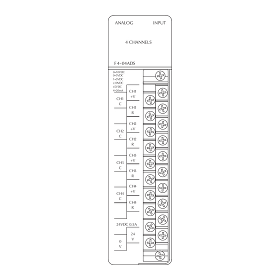
3–35 F4–04AD 4 Channel Analog Input Units Select Cross-Reference Units or Format D4-04AD F4-04AD Switch Setting Jumper Settings Standard Binary SW3=ON Two’s Complement SW3=OFF Step 4: The DIP switches S1 and S2 on the D4-04AD correspond to the number of active channels Number of Active Channels jumpers on the F4-04AD. - Page 79 F4-04ADS 4-Channel Isolated Analog Input In This Chapter..Module Specifications Setting the Module Jumpers Connecting the Field Wiring Module Operation Writing the Control Program...
-
Page 80: Analog Input Configuration Requirements
Analog Input The F4–04ADS Analog Input module requires 16 discrete input points from the Configuration CPU. The module can be installed in any slot of a DL405 system, including remote Requirements bases. The limitations on the number of analog modules are: For local and expansion systems, the available power budget and discrete I/O points. -
Page 81: Input Specifications
4–3 F4-04ADS 4-Channel Isolated Analog Input The following tables provide the specifications for the F4-04ADS Analog Input Module. Review these specifications to ensure the module meets your application requirements. Input Number of Channels Specifications 0–5V, 0–10V, 1–5V, $5V, $10V, Input Ranges 0–20 mA, 4–20 mA Resolution 12 bit (1 in 4096) -
Page 82: Setting The Module Jumpers
4–4 F4-04ADS 4-Channel Isolated Analog Input Setting the Module Jumpers Jumper The module has several options that you can select by installing or removing jumpers. At the rear of the module are three banks of jumpers: Locations One bank of 16 jumpers, which may be configured to select the number of channels enabled, channel range (for channels 1–4), and polarity. -
Page 83: Selecting The Number Of Channels
4–5 F4-04ADS 4-Channel Isolated Analog Input Selecting the The jumpers labeled 0 and 1 are used to Number of select the number of channels that will be Channels used. The module is set from the factory for Number of four-channel operation. Channels Any unused channels are not processed. - Page 84 4–6 F4-04ADS 4-Channel Isolated Analog Input The following tables show the jumper selections for the various ranges. Only channel 1 is used in the example, but all the channels must be set. You can have a combination of offsets and ranges but not polarities for each of the channels. For example, if the polarity is set for unipolar signal range, this setting will apply to all active channels.
-
Page 85: Connecting The Field Wiring
4–7 F4-04ADS 4-Channel Isolated Analog Input Connecting the Field Wiring Wiring Your company may have guidelines for wiring and cable installation. If so, you Guidelines should check those before you begin the installation. Here are some general things to consider. Use the shortest wiring route whenever possible. -
Page 86: Current Loop Transmitter Impedance
4–8 F4-04ADS 4-Channel Isolated Analog Input Current Loop Standard 4 to 20 mA transmitters and transducers can operate from a wide variety Transmitter of power supplies. Not all transmitters are alike and the manufacturers often specify Impedance a minimum loop or load resistance that must be used with the transmitter. The F4-04ADS provides 250 ohms resistance for each channel. -
Page 87: Module Operation
4–9 F4-04ADS 4-Channel Isolated Analog Input Module Operation DL430 Special Even though the module can be placed in any slot, it is important to examine the Requirements configuration if you are using a DL430 CPU. As you can see in the section on writing the program, you use V-memory locations to extract the analog data. -
Page 88: Channel Scanning Sequence
4–10 F4-04ADS 4-Channel Isolated Analog Input Before you begin writing the control program, it is important to take a few minutes to understand how the module processes and represents the analog signals. Channel The F4-04ADS module supplies one channel of data per each CPU scan. Since Scanning there are four channels, it can take up to four scans to get data for all channels. -
Page 89: Input Bit Assignments
4–11 F4-04ADS 4-Channel Isolated Analog Input Input Bit The F4-04ADS module requires 16 discrete input points from the CPU. These 16 Assignments points provide: an indication of which channel is active. the digital representation of the analog signal. Since all input points are automatically mapped into V-memory, it is very easy to determine the location of the data word that will be assigned to the module. -
Page 90: Analog Data Bits
4–12 F4-04ADS 4-Channel Isolated Analog Input Analog Data Bits The first twelve bits represent the analog data in binary format. V40401 Value Value 9 8 7 6 5 4 3 2 1 – data bits 1024 2048 Since the module has 12-bit resolution, the analog signal is converted into 4096 counts ranging from 0 –... -
Page 91: Writing The Control Program
4–13 F4-04ADS 4-Channel Isolated Analog Input Writing the Control Program Once you have configured the F4–04ADS module, use the following examples to get started writing the control program. Multiple Since all channels are multiplexed into a single data word, the control program must Channels be setup to determine which channel is being read. -
Page 92: Reading Values, Dl430
4–14 F4-04ADS 4-Channel Isolated Analog Input Reading Values, The following program example shows how to read the analog data into V-memory DL430 locations with the DL430 CPU. Since the DL430 does not support the LDF instruction, you can use the LD instruction instead as shown. The example also works for DL440 and DL450 CPUs. -
Page 93: Reading Four Channels In One Scan, Dl440/450 Only
4–15 F4-04ADS 4-Channel Isolated Analog Input Reading Four The following program shows you how to read all four channels in one scan by using Channels in a FOR/NEXT loop. Remember, this routine will lengthen the scan time. If you do not One Scan, need to read the analog data on every scan, change the SP1 to a permissive contact (such as X input, CR, or stage bit) to only enable the loop when it is required. - Page 94 4–16 F4-04ADS 4-Channel Isolated Analog Input Analog Value of 2024, slightly less than half scale, should yield 49.4 PSI Example without multiplier Example with multiplier Units + A H * L Units + 10 A H * L 4095 4095 Units + 2024 100 * 0 Units + 20240 100 * 0 4095...
-
Page 95: Analog And Digital Value Conversions
4–17 F4-04ADS 4-Channel Isolated Analog Input Analog and Sometimes it is helpful to be able to quickly convert between the signal levels and Digital Value the digital values. This is especially useful during machine startup or Conversions troubleshooting. The following table provides formulas to make this conversion easier. - Page 96 F4-08AD 8-Channel Analog Input In This Chapter..Module Specifications Setting the Module Jumpers Connecting the Field Wiring Module Operation Writing the Control Program...
-
Page 97: Module Specifications
24VDC 0.1A Analog Input The F4–08AD Analog Input module requires 16 discrete input points. The module can be installed in any slot of a DL405 system, including remote bases. The Configuration Requirements limitations on the number of analog modules are: For local and expansion systems, the available power budget and discrete I/O points. -
Page 98: Input Specifications
5–3 F4–08AD 8-Channel Analog Input The following table provides the specifications for the F4–08AD Analog Input Module. Review these specifications to ensure the module meets your application requirements. Input Number of Channels 8, single ended (one common) Specifications 0–5V, 0–10V, 1–5V, $5V, $10V, Input Ranges 0–20 mA, 4–20 mA Resolution... -
Page 99: Setting The Module Jumpers
5–4 F4–08AD 8-Channel Analog Input Setting the Module Jumpers Jumper If you examine the rear of the module, you will notice four banks of jumpers. The Locations module has several options that you can select by installing or removing these jumpers: A bank of eight jumpers to set voltage or current input for each channel. -
Page 100: Selecting Current Or Voltage
5–5 F4–08AD 8-Channel Analog Input Selecting Notice the eight jumpers for selecting current or voltage settings for each individual channel. For each channel install the jumper when you are using a current input or Current or Voltage remove the jumper if using a voltage input. Selecting Input The following table shows the jumper selections for the various ranges and are Signal and... -
Page 101: Connecting The Field Wiring
Check local and national codes to choose the correct method for your application. User Power The F4-08AD module requires a separate power supply. The Series DL405 CPUs, D4-RS Remote I/O Controller, and D4-EX Expansion Units have built-in 24 VDC Supply power supplies that provide up to 400mA of current. -
Page 102: Current Loop Transmitter Impedance
5–7 F4–08AD 8-Channel Analog Input Current Loop Standard 4 to 20 mA transmitters and transducers can operate from a wide variety Transmitter of power supplies. Not all transmitters are alike and the manufacturers often specify Impedance a minimum loop or load resistance that must be used with the transmitter. The F4-08AD provides 250 ohm resistance for each channel. -
Page 103: Wiring Diagram
5–8 F4–08AD 8-Channel Analog Input Wiring Diagram NOTE 1: Shields should be grounded at the signal source. NOTE 2: Unused channels should be connected to 0V or have current jumpers installed. Internal ANALOG INPUT Module See NOTE 1 Wiring 250 ohms 8 CHANNELS Voltage –... -
Page 104: Module Operation
5–9 F4–08AD 8-Channel Analog Input Module Operation DL430 Special Even though the module can be placed in any slot, it is important to examine the Requirements configuration if you are using a DL430 CPU. As you will see in the section on writing the program, you use V-memory locations to extract the analog data. -
Page 105: Channel Scanning Sequence
5–10 F4–08AD 8-Channel Analog Input Before you begin writing the control program, it is important to take a few minutes to understand how the module processes and represents the analog signals. Channel The F4-08AD module supplies one channel of data per each CPU scan. Since Scanning there are eight channels, it can take up to eight scans to get data for all channels. -
Page 106: Input Bit Assignments
5–11 F4–08AD 8-Channel Analog Input Input Bit You may recall the F4–08AD module requires 16 discrete input points from the Assignments CPU. These 16 points provide: An indication of which channel is active. The digital representation of the analog signal. Since all input points are automatically mapped into V-memory, it is very easy to determine the location of the data word that will be assigned to the module. -
Page 107: Analog Data Bits
5–12 F4–08AD 8-Channel Analog Input Analog Data Bits The first twelve bits represent the analog data in binary format. V40401 Value Value 9 8 7 6 5 4 3 2 1 – data bits 1024 2048 Since the module has 12-bit resolution, the analog signal is converted into 4096 counts ranging from 0-4095 (2 ). -
Page 108: Writing The Control Program
5–13 F4–08AD 8-Channel Analog Input Writing the Control Program If you have configured the F4–08AD module, use the following examples to get started writing the control program. Multiple Since all channels are multiplexed into a single data word, the control program must Channels be set up to determine which channel is being read. -
Page 109: Reading Values, Dl430 Cpu
KFFF Since the DL405 CPUs perform math operations in BCD, it is usually best to convert the data to BCD immediately. You can leave out this instruction if your application does not require it (such as for PID loops, which require the process variable to be in binary format). -
Page 110: Single Channel Selected
5–15 F4–08AD 8-Channel Analog Input Single Channel Since you do not have to determine which channel is selected, the single channel Selected program is even more simple. When X34 is on, channel 1 data is being sent to the CPU. Use the LD or LDF LD instruction when using a DL430 CPU.* The BCD instruction converts the data from binary to BCD. -
Page 111: Reading Eight Channels In One Scan, Dl440/450
The LDIF instruction will retreive the I/O points without waiting on the CPU to finish the scan. Since the DL405 CPUs perform math operations in BCD, it is usually best to convert the data to BCD immediately. You can leave out this instruction if your application does not require it (such as PID loops). - Page 112 5–17 F4–08AD 8-Channel Analog Input Analog Value of 2024, slightly less than half scale, should yield 49.4 PSI Example without multiplier Example with multiplier Units + 10 A H * L Units + A H * L 4095 4095 Units + 20240 100 * 0 Units + 2024 100 * 0 4095 4095...
-
Page 113: Analog And Digital Value Conversions
5–18 F4–08AD 8-Channel Analog Input Analog and Sometimes it is helpful to be able to quickly convert between the signal levels and Digital Value the digital values. This is especially useful during machine startup or Conversions troubleshooting. The following table provides formulas to make this conversion easier. - Page 114 F4–16AD–1 16-Channel Analog Input In This Chapter..Module Specifications Setting the Module Jumpers Connecting the Field Wiring Module Operation Writing the Control Program...
-
Page 115: Chapter 6: F4-16Ad-1 16-Channel Analog Input
24VDC @0.1A F4–16AD–1 Analog Input The F4–16AD–1 Analog Input module requires 16 discrete input points. The module can be installed in any slot of a DL405 system, including remote bases. The Configuration Requirements limitations on the number of analog modules are: For local and expansion systems, the available power budget and discrete I/O points. -
Page 116: Input Specifications
6–3 F4–16AD–1 16-Channel Analog Input The following table provides the specifications for the F4–16AD–1 Analog Input Module. Review these specifications to ensure the module meets your application requirements. Input Number of Channels 16, single ended (one common) Specifications Input Ranges 0–20 mA, 4–20 mA Resolution 12 bit (1 in 4096) -
Page 117: Setting The Module Jumpers
6–4 F4–16AD–1 16-Channel Analog Input Setting the Module Jumpers Jumper If you examine the rear of the module, you will notice two banks of jumpers. The Locations module has several options that you can select by installing or removing jumpers: A bank of two jumpers sets the current input range for the 16 channels (channels 1–8 and 9–16). -
Page 118: Selecting The Number Of Channels
6–5 F4–16AD–1 16-Channel Analog Input Selecting the The jumpers labeled +1, +2, +4 and +8 +8 +4 +2 Number of are used to select the number of Channels channels that will be used. Any unused channels are not processed so if you only select channels 1–8, then the last eight channels will not be active. -
Page 119: Connecting The Field Wiring
Check local and national codes to choose the correct method for your application. User Power The F4–16AD–1 module requires a separate power supply. The Series DL405 CPUs, D4-RS Remote I/O Controller, and D4-EX Expansion Units have built-in 24 Supply VDC power supplies that provide up to 400mA of current. -
Page 120: Current Loop Transmitter Impedance
6–7 F4–16AD–1 16-Channel Analog Input Current Loop Standard 4 to 20 mA transmitters and transducers can operate from a wide variety Transmitter of power supplies. Not all transmitters are alike and manufacturers often specify a Impedance minimum loop or load resistance that must be used with the transmitter. The F4–16AD–1 provides 250 ohm resistance for each channel. -
Page 121: Removable Connector
6–8 F4–16AD–1 16-Channel Analog Input Removable The F4–16AD–1 module has a removable connector to make wiring easier. Simply Connector remove the retaining screws and gently pull the connector from the module. Wiring Diagram NOTE 1: Shields should be grounded at the signal source. Internal ANALOG INPUT... -
Page 122: Module Operation
6–9 F4–16AD–1 16-Channel Analog Input Module Operation DL430 Special Even though the module can be placed in any slot, it is important to examine the Requirements configuration if you are using a DL430 CPU. As you will see in the section on writing the program, you use V-memory locations to extract the analog data. -
Page 123: Channel Scanning Sequence
6–10 F4–16AD–1 16-Channel Analog Input Before you begin writing the control program, it is important to take a few minutes to understand how the module processes and represents the analog signals. Channel The F4–16AD–1 module supplies one channel of data per each CPU scan. Since Scanning there are 16 channels, it can take up to 16 scans to get data for all channels. -
Page 124: Input Bit Assignments
6–11 F4–16AD–1 16-Channel Analog Input Input Bit You may recall the F4–16AD–1 module requires 16 discrete input points from the Assignments CPU. These 16 points provide: An indication of which channel is active. The digital representation of the analog signal. Since all input points are automatically mapped into V-memory, it is very easy to determine the location of the data word that will be assigned to the module. -
Page 125: Analog Data Bits
6–12 F4–16AD–1 16-Channel Analog Input Analog Data Bits The first twelve bits represent the analog data in binary format. V40401 Value Value 9 8 7 6 5 4 3 2 1 – data bits 1024 2048 Since the module has 12-bit resolution, the analog signal is converted into 4096 counts ranging from 0-4095 (2 ). -
Page 126: Writing The Control Program
6–13 F4–16AD–1 16-Channel Analog Input Writing the Control Program If you have configured the F4–16AD–1 module, use the following examples to get started writing the control program. Multiple Since all channels are multiplexed into a single data word, the control program must Channels be set up to determine which channel is being read. -
Page 127: Reading Values, Dl430 Cpu
KFFF Since the DL405 CPUs perform math operations in BCD, it is usually best to convert the data to BCD immediately. You can leave out this instruction if your application does not require it (such as for PID loops, which require the process variable to be in binary format). - Page 128 6–15 F4–16AD–1 16-Channel Analog Input Single Channel Since you do not have to determine which channel is selected, the single channel Selected program is even more simple. When X34 is on, channel 1 data is being sent to the CPU. Use the LD or LDF LD instruction when using a DL430 CPU.* The BCD instruction converts the data from binary to BCD.
-
Page 129: Reading Sixteen Channels In One Scan
The LDIF instruction will retreive the I/O points without waiting on the CPU to finish the scan. Since the DL405 CPUs perform math operations in BCD, it is usually best to convert the data to BCD immediately. You can leave out this instruction if your application does not require it (such as PID loops). - Page 130 6–17 F4–16AD–1 16-Channel Analog Input Analog Value of 2024, slightly less than half scale, should yield 49.4 PSI Example without multiplier Example with multiplier Units + 10 A H * L Units + A H * L 4095 4095 Units + 20240 100 * 0 Units + 2024 100 * 0 4095 4095...
-
Page 131: Analog And Digital Value Conversions
6–18 F4–16AD–1 16-Channel Analog Input Analog and Sometimes it is helpful to be able to quickly convert between the signal levels and Digital Value the digital values. This is especially useful during machine startup or Conversions troubleshooting. The following table provides formulas to make this conversion easier. - Page 132 F4–16AD–2 Incorrect - this is a 8-Channel 16-point analog input Analog Input In This Chapter..Module Specifications Setting the Module Jumpers Connecting the Field Wiring Module Operation Writing the Control Program...
-
Page 133: Module Specifications
24VDC @0.1A F4–16AD–2 Analog Input The F4–16AD–2 Analog Input module requires 16 discrete input points. The module can be installed in any slot of a DL405 system, including remote bases. The Configuration Requirements limitations on the number of analog modules are: For local and expansion systems, the available power budget and discrete I/O points. -
Page 134: Input Specifications
7–3 F4–16AD–2 16-Channel Analog Input The following table provides the specifications for the F4–16AD–2 Analog Input Module. Review these specifications to ensure the module meets your application requirements. Input Number of Channels 16, single ended (one common) Specifications Input Ranges 0–5V, 0–10V Resolution 12 bit (1 in 4096) -
Page 135: Setting The Module Jumpers
7–4 F4–16AD–2 16-Channel Analog Input Setting the Module Jumpers Jumper If you examine the rear of the module, you will notice two banks of jumpers. The Locations module has several options that you can select by installing or removing these jumpers: A bank of two jumpers to set voltage input range for each bank of 8 channels. -
Page 136: Selecting The Number Of Channels
7–5 F4–16AD–2 16-Channel Analog Input Selecting the The jumpers labeled +1, +2, +4 and +8 +8 +4 +2 Number of are used to select the number of Channels channels that will be used. Any unused channels are not processed so if you only select channels 1–8, then the last eight channels will not be active. -
Page 137: Connecting The Field Wiring
Check local and national codes to choose the correct method for your application. User Power The F4–16AD–2 module requires a separate power supply. The Series DL405 CPUs, D4-RS Remote I/O Controller, and D4-EX Expansion Units have built-in 24 Supply VDC power supplies that provide up to 400mA of current. -
Page 138: Custom Input Ranges
7–7 F4–16AD–2 16-Channel Analog Input Custom Input Occasionally you may have the need to connect a transmitter with an unusual signal range. By changing the wiring slightly and adding an external resistor to Ranges convert the current to voltage, you can easily adapt this module to meet the specifications for a transmitter that does not adhere to one of the standard input ranges. -
Page 139: Removable Connector
7–8 F4–16AD–2 16-Channel Analog Input Removable The F4–16AD–2 module has a removable connector to make wiring easier. Simply Connector remove the retaining screws and gently pull the connector from the module. Wiring Diagram NOTE 1: Shields should be grounded at the signal source. Internal ANALOG INPUT... -
Page 140: Module Operation
7–9 F4–16AD–2 16-Channel Analog Input Module Operation D4–430 Special Even though the module can be placed in any slot, it is important to examine the Requirements configuration if you are using a D4–430 CPU. As you will see in the section on writing the program, you use V-memory locations to extract the analog data. -
Page 141: Channel Scanning Sequence
7–10 F4–16AD–2 16-Channel Analog Input Before you begin writing the control program, it is important to take a few minutes to understand how the module processes and represents the analog signals. Channel The F4–16AD–2 module supplies one channel of data per each CPU scan. Since Scanning there are sixteen channels, it can take up to sixteen scans to get data for all Sequence... -
Page 142: Input Bit Assignments
7–11 F4–16AD–2 16-Channel Analog Input Input Bit You may recall the F4–16AD–2 module requires 16 discrete input points from the Assignments CPU. These 16 points provide: An indication of which channel is active. The digital representation of the analog signal. Since all input points are automatically mapped into V-memory, it is very easy to determine the location of the data word that will be assigned to the module. -
Page 143: Analog Data Bits
7–12 F4–16AD–2 16-Channel Analog Input Analog Data Bits The first twelve bits represent the analog data in binary format. V40401 Value Value 9 8 7 6 5 4 3 2 1 – data bits 1024 2048 Since the module has 12-bit resolution, the analog signal is converted into 4096 counts ranging from 0-4095 (2 ). -
Page 144: Writing The Control Program
7–13 F4–16AD–2 16-Channel Analog Input Writing the Control Program If you have configured the F4–16AD–2 module, use the following examples to get started writing the control program. Multiple Since all channels are multiplexed into a single data word, the control program must Channels be set up to determine which channel is being read. -
Page 145: Reading Values
KFFF Since the DL405 CPUs perform math operations in BCD, it is usually best to convert the data to BCD immediately. You can leave out this instruction if your application does not require it (such as for PID loops, which require the process variable to be in binary format). -
Page 146: Single Channel Selected
7–15 F4–16AD–2 16-Channel Analog Input Single Channel Since you do not have to determine which channel is selected, the single channel Selected program is even more simple. When X34 is on, channel 1 data is being sent to the CPU. Use the LD or LDF LD instruction when using a D4–430 CPU.* The BCD instruction converts the data from binary to BCD. -
Page 147: Reading Sixteen Channels In One Scan
The LDIF instruction will retreive the I/O points without waiting on the CPU to finish the scan. Since the DL405 CPUs perform math operations in BCD, it is usually best to convert the data to BCD immediately. You can leave out this instruction if your application does not require it (such as PID loops). - Page 148 7–17 F4–16AD–2 16-Channel Analog Input Analog Value of 2024, slightly less than half scale, should yield 49.4 PSI Example without multiplier Example with multiplier Units + 10 A H * L Units + A H * L 4095 4095 Units + 20240 100 * 0 Units + 2024 100 * 0 4095 4095...
-
Page 149: Analog And Digital Value Conversions
7–18 F4–16AD–2 16-Channel Analog Input Analog and Sometimes it is helpful to be able to quickly convert between the signal levels and the digital values. This is especially useful during machine startup or Digital Value Conversions troubleshooting. The following table provides formulas to make this conversion easier. -
Page 150: Chapter 8: F4-08Thm-N 8-Channel Thermocouple Input
F4-08THM-n 8-Channel Thermocouple Input In This Chapter..Module Specifications Setting the Module Jumpers Connecting the Field Wiring Module Operation Writing the Control Program... -
Page 151: Module Specifications
8–2 F4–08THM–n 8-Channel Thermocouple Input Module Specifications The F4–08THM–n 8-Channel Thermocouple Input module TEMPERATURE INPUT provides several features and benefits. THERMOCOUPLE It provides eight thermocouple input channels with F4–08THM 12-bit resolution. It automatically converts type E, K, R, S, J, B, C, P or T thermocouple signals into direct temperature CH1 –... -
Page 152: Input Specifications
8–3 F4–08THM–n 8-Channel Thermocouple Input The following table provides the specifications for the F4–08THM–n Thermocouple Input Module. Review these specifications to ensure the module meets your application requirements. Input Number of Channels 8, differential inputs Specifications Type E: –270/1000 _C, –450/1832 _F Input Ranges Type J: –210/760 _C,... -
Page 153: Module Calibration
Thermocouple The F4–08THM–n Thermocouple Input Module requires16 discrete input points Input from the CPU. The module can be installed in any slot of a DL405 system, including Configuration remote bases. The limitations on the number of analog modules are: Requirements For local and expansion systems, the available power budget and discrete I/O points. -
Page 154: Selecting The Number Of Channels
8–5 F4–08THM–n 8-Channel Thermocouple Input Selecting the The three jumpers closest to the top of Number of the module are binary encoded to select the number of channels that will be used. Channels Number of Channels must be used contiguously, Active starting with channel 1. -
Page 155: Selecting Temperature Or Counts
8–6 F4–08THM–n 8-Channel Thermocouple Input Selecting The jumper closest to the bottom of the Temperature module selects between conversion to units of temperature or to a binary count or Counts ranging from 0 to 4094. For Temperature format, remove the jumper. -
Page 156: Wiring Diagram
8- -7 F4--08THM--n 8-Channel Thermocouple Input Wiring Diagram Note 1: Terminate shields at the respective signal source. Note 2: Leave unused channels open (no connection). Internal Module Wiring TEMPERATURE INPUT THERMOCOUPLE See Note 1 F4--08THM--n CH1 - - Examples of differential CH1+ Thermocouple wiring CH2- -... -
Page 157: Module Operation
8–8 F4–08THM–n 8-Channel Thermocouple Input Module Operation Before you begin writing the control program, it is important to take a few minutes to understand how the module processes and represents the analog signals. DL430 Special Even though the module can be placed in any slot, it is important to examine the configuration if you are using a DL430 CPU. -
Page 158: Channel Scanning Sequence
8–9 F4–08THM–n 8-Channel Thermocouple Input Channel The F4–08THM–n module supplies one channel of data per each CPU scan. Since there are eight channels, it can take up to eight scans to get data for all channels. Scanning Sequence Once all channels have been scanned the process starts over with channel 1. There are ways around this and later we will show you how to write a program that will get all eight channels in one scan. -
Page 159: Identifying The Data Locations
8–10 F4–08THM–n 8-Channel Thermocouple Input Identifying the You may recall the Thermocouple Input module requires 16 discrete input points from the CPU. These 16 points provide: Data Locations An indication of which channel is active. The digital representation of the signal. Since all input points are automatically mapped into V-memory, it is very easy to determine the location of the data word that will be assigned to the module. -
Page 160: Analog Data Bits
8–11 F4–08THM–n 8-Channel Thermocouple Input Temperature Sign The most significant bit is used to note V40401 the sign of the temperature. If this bit is on, then the temperature is negative. If the bit is off, then the temperature is 9 8 7 6 5 4 3 2 1 positive. - Page 161 8–12 F4–08THM–n 8-Channel Thermocouple Input Writing the Control Program Multiple Since all channels are multiplexed into a single data word, the control program must Channels be setup to determine which channel is being read. Since the module appears as X input points to the CPU, it is very easy to use the active channel status bits to Selected demultiplex the individual channel information...
- Page 162 KFFF Since the DL405 CPUs perform math operations in BCD, it is usually best to convert the data to BCD immediately. You can leave out this instruction if your application does not require it (such as for PID loops, which require the process variable to be in binary format).
- Page 163 8–14 F4–08THM–n 8-Channel Thermocouple Input Single Channel Since you do not have to determine which channel is selected, the single channel Selected program is even more simple. Channel 1 data is being sent to the CPU. Use the LD instruction LD or LDF when using a DL430 CPU.* The BCD instruction converts the data from binary to BCD.
- Page 164 The LDIF instruction will retreive the I/O points without waiting on the CPU to finish the scan. Since the DL405 CPUs perform math operations in BCD, it is usually best to convert the data to BCD immediately. You can leave out this instruction if your application does not require it (such as PID loops).
- Page 165 8–16 F4–08THM–n 8-Channel Thermocouple Input Using the Sign By adding a couple of simple rungs you can easily monitor the temperature for positive vs. negative readings. For example, if you have to know whether the Bit, DL440/450 temperature is +100 _F or –100 _F, an easy way to do this is to use the channel indicator inputs and the sign bit to set a control relay when the temperature is negative.
- Page 166 8–17 F4–08THM–n 8-Channel Thermocouple Input Scaling the Input The Thermocouple Input module automatically converts the temperature readings into the digital equivalent, so as long as you are using the module to monitor Data temperatures you never have to perform any scaling. However, there are two situations where you will probably want to understand how to scale the data.
- Page 167 8–18 F4–08THM–n 8-Channel Thermocouple Input Loads the first 12 bits of the channel data word into the accumulator. The X address depends on the I/O configuration. Since we are going to perform some math operations in BCD, this instruction converts the data format. This LDF instruction loads the three channel indicator bits, plus the MSB, into the accumulator.
- Page 168 F4-08RTD 8-Channel RTD Input In This Chapter..Module Specifications Setting the Module Jumpers Connecting the Field Wiring Module Operation Writing the Control Program...
-
Page 169: Module Specifications
RTD Input The F4–08RTD Input Module requires 32 discrete input points from the CPU. The Configuration module can be installed in any slot of a DL405 system, including remote bases. The limitations on the number of analog modules are: Requirements For local and expansion systems, the available power budget and discrete I/O points. - Page 170 9–3 F4–08RTD 8-Channel RTD Input The following tables provide the specifications for the F4–08RTD Module. Review these specifications to ensure the module meets your application requirements. Input Number of Channels 8 differential inputs Specifications Input Ranges Pt100 –200°C/850°C (–328°F/1562°F) Pt 1000 –200°C/595°C (–328°F/1103°F) jPt100 –38°C/450°C (–36°F/842°F)
-
Page 171: Setting The Module Jumpers
9–4 F4–08RTD 8-Channel RTD Input Setting the Module Jumpers Jumper Locations The module has several options that you can select by installing or removing jumpers. At the rear of the module is a bank of eight jumpers. You can select the following options by installing or removing the jumpers: Number of channels: 1 thru 8. - Page 172 9–5 F4–08RTD 8-Channel RTD Input The two’s complement data format may be required to correctly display bipolar data on some operator interfaces and HMI software packages. This data format could also be used to simplify averaging a bipolar signal. The table shows how to arrange the jumpers. X = jumper installed, empty space = jumper removed.
-
Page 173: Selecting The Number Of Channels
9–6 F4–08RTD 8-Channel RTD Input Selecting the The three jumpers labeled CH+4, CH+2, and CH+1 are binary encoded to select Number of the number of channels that will be used. Channels Channels must be used sequentially, starting with channel 1. For example, if you are going to use only two channels, you must use channels 1 and 2 (not 2 and 3, 5 and 7, etc.). -
Page 174: Connecting The Field Wiring
9–7 F4–08RTD 8-Channel RTD Input Connecting the Field Wiring Wiring Guidelines Your company may have guidelines for wiring and cable installation. If so, you should check those before you begin the installation. Here are some general things to consider. Use the shortest wiring route whenever possible. Use shielded wiring and ground the shield at the signal source. -
Page 175: Wiring Diagram
9–8 F4–08RTD 8-Channel RTD Input Wiring Diagram The F4–08RTD module has a removable connector to make wiring easier. Simply remove the retaining screws and gently pull the connector from the module. RTD INPUT Note 1 200 µA Ch1 + 8 CHANNELS Ch1 −... -
Page 176: Module Operation
9–9 F4–08RTD 8-Channel RTD Input Module Operation DL430 Special Even though the module can be placed in any slot, it is important to examine the Requirements configuration if you are using a DL430 CPU. As you will see in the section on writing the program, you use V-memory locations to extract the analog data. -
Page 177: Channel Scanning Sequence
9–10 F4–08RTD 8-Channel RTD Input Channel Scanning Before you begin writing the control program, it is important to take a few minutes to Sequence understand how the module processes and represents the analog signals. The F4–08RTD module supplies one channel of data per each CPU scan. Since there are eight channels, it can take up to eight scans to get data for all channels. - Page 178 9–11 F4–08RTD 8-Channel RTD Input Identifying the The F4–08RTD module requires 32-point discrete input points. These inputs Data Locations provide: Individual active channel bits for each channel. A digital representation of the analog signal in various data formats. Individual broken transmitter detection bits for each channel. Since all input points are automatically mapped into V-memory, it is very easy to determine the location of the two data words that will be assigned to the module.
-
Page 179: Writing The Control Program
9–12 F4–08RTD 8-Channel RTD Input Writing the Control Program After you have configured the F4–08RTD module, use the following examples to get started writing the control program. The analog data is multiplexed into the lower word and is presented in 16 bits. The Multiple Active upper word contains three groups of bits that contain active channel status, unused Channels... -
Page 180: Active Channel Bits
9–13 F4–08RTD 8-Channel RTD Input Active The active channel bits represent the V40402 Channel channel selections in binary format (000 = channel 1 is active, 001 = Bits channel 2 is active, 111 = channel 8 is = active channel bits active, etc.). -
Page 181: Reading Values, Dl440/450
9–14 F4–08RTD 8-Channel RTD Input Reading Values, The following program example shows how to read the analog data into V-memory DL440/450 locations with DL440 and DL450 CPUs. Once the data is in V-memory, you can perform math on the data, compare the data against preset values, and so forth. This example will read one channel per scan, so it will take eight scans to read all eight channels. - Page 182 9–15 F4–08RTD 8-Channel RTD Input Reading Eight The following program example shows how to read all eight channels in one scan by Channels in using a FOR/NEXT loop. This program only works with DL440 and DL450 CPUs. Before you try this method, remember that the FOR/NEXT routine shown here will One Scan, add about 10–12 ms to the overall scan time.
-
Page 183: Using Bipolar Ranges (Magnitude Plus Sign)
9–16 F4–08RTD 8-Channel RTD Input Using Bipolar With bipolar ranges, you need some additional logic because you need to know if the Ranges value being returned represents a positive voltage or a negative voltage. For example, you may need to know if the temperature is positive or negative. (Magnitude Plus Sign) The following program shows how you can accomplish this. -
Page 184: Using Bipolar Ranges Example Continued
9–17 F4–08RTD 8-Channel RTD Input Using Bipolar Store Channel 4 Ranges Example Continued This rung looks at fault bit X33 (the broken OUTD transmitter bit for channel 4) ANDed with V3006 active channel bits X20–X22. When the active channel bits are true and there is no C103 transmitter fault, channel 4 data is stored in V3006. - Page 185 F4-08THM 8-Channel Thermocouple Input In This Chapter..Module Specifications Setting The Module Jumpers Connecting the Field Wiring Module Operation Writing the Control Program...
-
Page 186: Module Specifications
10–2 F4-08THM 8-Channel Thermocouple Input Module Specifications The F4-08THM 8-Channel Thermocouple Input Module TEMPERATURE INPUT provides several features and benefits. THERMOCOUPLE Eight thermocouple input channels with 16-bit F4–08THM voltage resolution or 0.1 _C/_F temperature resolution. CH1 – Automatically converts type E, J, K, R, S, T, B, N, or CH1+ CH2–... - Page 187 .01 _C. Thermocouple The F4-08THM module requires 32 discrete input points from the CPU. The module can be installed in any slot of a DL405 system. The limitations on the number of Input Configuration analog modules are:...
- Page 188 10–4 F4-08THM 8-Channel Thermocouple Input Setting the Module Jumpers Jumper Use the figure on the following page to locate the bank of ten jumpers on the PC board. Notice that the description of each jumper is just to the right of the jumpers on Locations the PC board.
- Page 189 10–5 F4-08THM 8-Channel Thermocouple Input Selecting the The next three jumpers labeled CH+1, CH+2, and CH+4 determine the number of Number of channels that will be used. The table shows how to set the jumpers for channels 1 thru 8. Channels The module comes with three jumpers installed for eight channel operation.
-
Page 190: Setting Input Type
10–6 F4-08THM 8-Channel Thermocouple Input Setting Input Type The next four jumpers (Tc Type 0, Tc Type 1, Tc Type 2, Tc Type 3) must be set to match the type of thermocouple being used or the input voltage level. The module can be used with many types of thermocouples. -
Page 191: Voltage Conversion Units
10–7 F4-08THM 8-Channel Thermocouple Input For unipolar thermocouple ranges (R,S,B,C), it does not matter if magnitude plus sign or 2’s complement is selected. Use the table to select settings. The module comes with both jumpers installed for magnitude plus sign conversion in Fahrenheit. For example, remove the Units-0 jumper and leave the Units-1 jumper installed for magnitude plus sign conversion in Celsius. -
Page 192: Connecting The Field Wiring
The DL405 base has a switching type power supply. As a result of switching noise, you may notice some instability in the analog input data if you use the base power supply. -
Page 193: Thermocouples
10–9 F4-08THM 8-Channel Thermocouple Input Thermocouples Use shielded thermocouples whenever possible to minimize the presence of noise on the thermocouple wire. Ground the shield wire at one end only. For grounded thermocouples, connect the shield at the sensor end. For ungrounded thermocouples, connect the shield to the 0V (common) terminal. -
Page 194: Wiring Diagram
10- -10 F4-08THM 8-Channel Thermocouple Input Wiring Diagram Use the following diagrams to connect the field wiring. Thermocouple Input Wiring Diagram TEMPERATURE INPUT THERMOCOUPLE CH1-- CH1+ CH2-- CH2+ CH3-- CH3+ CH4-- CH4+ CH5-- CH5+ CH6-- CH6+ CH7-- CH7+ CH8-- CH8+ 24V@60mA Voltage Input Wiring Diagram See Errata Sheet at the... -
Page 195: Module Operation
10–11 F4-08THM 8-Channel Thermocouple Input Module Operation DL430 Special Even though the module can be placed in any slot, it is important to examine the Requirements configuration if you are using a DL430 CPU. As you will see in the section on writing the program, you use V-memory locations to extract the analog data. -
Page 196: Channel Scanning Sequence
10–12 F4-08THM 8-Channel Thermocouple Input Channel Scanning Before you begin writing the control program, it is important to take a few minutes to Sequence understand how the module processes and represents the analog signals. The F4–08THM module supplies one channel of data per each CPU scan. Since there are eight channels, it can take up to eight scans to get data for all channels. - Page 197 10–13 F4-08THM 8-Channel Thermocouple Input Identifying the The F4–08THM module requires 32-point discrete input points (five bits are Data Locations unused). These inputs provide: Three active channel bits A digital representation of the analog signal in 16 bits, including one sign bit.
-
Page 198: Writing The Control Program
10–14 F4-08THM 8-Channel Thermocouple Input Writing the Control Program After you have configured the F4–08THM module, use the following examples to get started writing the control program. Multiple Active The analog data is multiplexed into the lower word and is presented in 16 bits. The upper word contains three groups of bits that contain active channel status, unused Channels bits, and broken transmitter status. -
Page 199: Active Channel Bits
10–15 F4-08THM 8-Channel Thermocouple Input Active The active channel bits represent the V40402 channel selections in binary format Channel Bits (000 = channel 1 is active, 001 = channel 2 is active, 111 = channel 8 is = active channel bits active, etc.). -
Page 200: Reading Values, Dl440/450
10–16 F4-08THM 8-Channel Thermocouple Input Reading Values, The following program example shows how to read the analog data into V-memory DL440/450 locations with DL440 and DL450 CPUs. Once the data is in V-memory, you can perform math on the data, compare the data against preset values, and so forth. This example will read one channel per scan, so it will take eight scans to read all eight channels. - Page 201 10–17 F4-08THM 8-Channel Thermocouple Input Using Bipolar With bipolar ranges, you need some additional logic because you need to know if Ranges the value being returned represents a positive voltage or a negative voltage. For (Magnitude Plus example, you may need to know if the temperature is positive or negative. Sign) The following program shows how you can accomplish this.
-
Page 202: Using Bipolar Ranges Example Continued
10–18 F4-08THM 8-Channel Thermocouple Input Using Bipolar Ranges Example Continued Store Channel 4 This rung looks at fault bit X33 (the broken OUTD transmitter bit for channel 4) ANDed with V3006 active channel bits X20–X22. When the active channel bits are true and there is no C103 transmitter fault, channel 4 data is stored in V3006. -
Page 203: Module Resolution16-Bit (Unipolar Voltage Input)
10–19 F4-08THM 8-Channel Thermocouple Input Module Resolution Unipolar analog signals are 156mV 16-Bit (Unipolar converted into 65536 counts Voltage Input) ranging from 0 to 65535 (2 For example, with a 0 to 156mV signal range, 78mV would be 430 440 450 32767. -
Page 204: Analog And Digital Value Conversions
10–20 F4-08THM 8-Channel Thermocouple Input Analog Sometimes it is useful to be able to quickly convert between the signal levels and and Digital the digital values. This is especially helpful during machine startup or troubleshooting. Remember, this module does not operate like other versions of Value analog input modules that you may be familiar with. - Page 205 D4-02DA 2-Channel Analog Output In This Chapter..Module Specifications Connecting the Field Wiring Module Operation Writing the Control Program...
-
Page 206: Analog Output Configuration Requirements
Analog Output The D4–02DA Analog Output requires 32 discrete output points from the CPU. The Configuration module can be installed in any slot of a DL405 system, including remote bases. The Requirements limitations on the number of analog modules are: For local and expansion systems, the available power budget and discrete I/O points. - Page 207 11–3 D4-02DA 2-Channel Analog Output The following table provides the specifications for the D4–02DA Analog Output Module. Review these specifications to ensure the module meets your application requirements. Output Number of Channels 2 (independent) Specifications Output Ranges 0–10V, 1–5V, 4–20 mA Resolution 12 bit (1 in 4096) Output Type...
-
Page 208: Connecting The Field Wiring
11–4 D4-02DA 2-Channel Analog Output Connecting the Field Wiring Wiring Guidelines Your company may have guidelines for wiring and cable installation. If so, you should check those before you begin the installation. Here are some general things to consider. Use the shortest wiring route whenever possible. Use shielded wiring and ground the shield at the module or the power supply return (0V). -
Page 209: Wiring Diagram
11–5 D4-02DA 2-Channel Analog Output Wiring Diagram The D4–02DA module has a removable connector to make wiring easier. Simply remove the retaining screws and gently pull the connector from the module. NOTE 1: Shields should be connected to the 0V terminal of the module or power supply. -
Page 210: Dl430 Special Requirements
11–6 D4-02DA 2-Channel Analog Output Module Operation DL430 Special Even though the module can be placed in any slot, it is important to examine the Requirements configuration if you’re using a DL430 CPU. As you’ll see in the section on writing the program, you use V-memory locations to extract the analog data. -
Page 211: Channel Scanning Sequence
11–7 D4-02DA 2-Channel Analog Output Before you begin writing the control program, it is important to take a few minutes to understand how the module processes and represents the analog signals. Channel Scanning The D4–02DA module updates both channels in the same scan. The control Sequence program updates the two channels of this module independent of each other and each channel does not have to be refreshed on every scan. -
Page 212: Output Bit Assignments
11–8 D4-02DA 2-Channel Analog Output Output Bit You may recall the D4–02DA module requires 32 discrete output points. These 32 Assignments points provide the digital representation of the analog signals. Since all output points are automatically mapped into V-memory, it is very easy to determine the location of the data word that will be assigned to the module. -
Page 213: Analog Data Bits
11–9 D4-02DA 2-Channel Analog Output Analog Data Bits The first twelve bits of each V-memory location represent the analog data in V40501 & V40502 binary format. The remaining four bits are not used and are ignored by the module. 9 8 7 6 5 4 3 2 1 Value Value –... -
Page 214: Writing The Control Program
11–10 D4-02DA 2-Channel Analog Output Writing the Control Program Update Either As mentioned earlier, you can update either channel or both channels during the same scan. Since the module does not have any channel select bits, you just simply Channel determine the location of the data word and send the data word to the output module whenever you need to update the data. - Page 215 V3000. Also, you have to perform this for both channels if you’re using different data for each channel. NOTE: The DL405 offers various instructions that allow you to perform math operations using binary, BCD, etc. It is usually easier to perform any math calculations in BCD and then convert the value to binary before you send the data to the module.
-
Page 216: Analog And Digital Value Conversions
11–12 D4-02DA 2-Channel Analog Output Analog and Digital Sometimes it is helpful to be able to quickly convert between the voltage or current Value Conversions signal levels and the digital values. This is especially useful during machine startup or troubleshooting. The following table provides formulas to make this conversion easier. - Page 217 F4–04DA 4-Channel Analog Output In This Chapter..Module Specifications Setting the Module Jumpers Connecting the Field Wiring Module Operation Writing the Control Program...
-
Page 218: Module Specifications
24VDC 0.1A The F4–04DA Analog Output appears as a 16-point discrete output module. The Analog Output module can be installed in any slot of a DL405 system, including remote bases. The Configuration Requirements limitations on the number of analog modules are: For local and expansion systems, the available power budget and discrete I/O points. - Page 219 12–3 F4–04DA 4-Channel Analog Output The following table provides the specifications for the F4–04DA Analog Output Module. Review these specifications to ensure the module meets your application requirements. Output Number of Channels Specifications 0–5V, 0–10V, $5V, $10V, 4–20 mA Output Ranges Resolution 12 bit (1 in 4096) Conversion Method...
-
Page 220: Setting The Module Jumpers
12–4 F4–04DA 4-Channel Analog Output Setting the Module Jumpers Jumper If you examine the rear of the module, you will notice several jumpers. These Locations jumpers are used to select the signal range for each channel. There is also a current jumper. -
Page 221: Selecting Special Signal Ranges
12–5 F4–04DA 4-Channel Analog Output Commonly Used Signal Ranges (continued) Unipolar Signal Range Current Jumper Current Jumper Installed Removed 4 to 20 mA Not supported with current jumper removed 0 to +5 VDC 0 to +10 VDC Selecting Special The F4–04DA module supports additional ranges that are not encountered very often. -
Page 222: Connecting The Field Wiring
12–6 F4–04DA 4-Channel Analog Output Special Signal Ranges (continued) Signal Range Current Jumper Current Jumper Installed Removed $2.5 VDC Not supported with current jumper installed 0 to +2.5 VDC Not supported with current jumper removed +1.25 to +6.25 VDC Not supported with current jumper installed +2.5 to +7.5 VDC... -
Page 223: Removable Connector
12–7 F4–04DA 4-Channel Analog Output Load Each channel can be wired independently for voltage or current. However, you cannot use both "10 VDC and 4–20 mA signals on the same module. Requirements Current loads must have an impedance between 0 and 1000 ohms. Voltage loads must have an impedance greater than 2K ohms. -
Page 224: Module Operation
12–8 F4–04DA 4-Channel Analog Output Module Operation DL430 Special Even though the module can be placed in any slot, it is important to examine the Requirements configuration if you are using a DL430 CPU. As you will see in the section on writing the program, you use V-memory locations to send the analog data. - Page 225 12–9 F4–04DA 4-Channel Analog Output Before you begin writing the control program, it is important to take a few minutes to understand how the module processes and represents the analog signals. Channel The F4–04DA module allows you to update the channels in any order. Your control program determines which channel gets updated on any given scan by turning off a Scanning Sequence...
-
Page 226: Output Bit Assignments
12–10 F4–04DA 4-Channel Analog Output Output Bit You may recall the F4–04DA module requires 16 discrete output points from the Assignments CPU. These points provide: The digital representation of the analog signal. Identification of the channel that is to receive the data. Since all output points are automatically mapped into V-memory, it is very easy to determine the location of the data word that will be assigned to the module. -
Page 227: Analog Data Bits
12–11 F4–04DA 4-Channel Analog Output Analog Data Bits The first twelve bits of the V-memory location represent the analog data in V40501 binary format. Value Value 9 8 7 6 5 4 3 2 1 – data bits 1024 2048 Since the module has 12-bit resolution, the analog signal is made of 4096 “pieces”... -
Page 228: Writing The Control Program
12–12 F4–04DA 4-Channel Analog Output Writing the Control Program Update Any As mentioned earlier, you can update any channel or any channels during the same Channel scan. The following diagram shows the data locations for an example system. You use the channel selection outputs to determine which channel gets updated (more on this later). - Page 229 V3000. Also, you have to perform this for all four channels if you are using different data for each channel. NOTE: The DL405 offers various instructions that allow you to perform math operations using binary, BCD, etc. It is usually easier to perform any math calculations in BCD and then convert the value to binary before you send the data to the module.
-
Page 230: Sending Data To One Channel
12–14 F4–04DA 4-Channel Analog Output Sending Data to The following programs show you how to update a single channel. Notice the One Channel DL440 and DL450 CPUs require slightly different programs than the DL430 CPU. Since the DL430 does not support the OUTF instruction, the program must be modified to make sure the channel select bits are not accidentally changed by the data in the accumulator. - Page 231 12–15 F4–04DA 4-Channel Analog Output Sending the The following programs show you how to update all channels with the same data. Same Data to The primary difference from the previous example programs is that you do not have All Channels to include the channel selection bits.
-
Page 232: Sequencing The Channel Updates
12–16 F4–04DA 4-Channel Analog Output Sequencing The next four example programs show you how to send digital values to the module the Channel when you have more than one channel. These examples will automatically update Updates all four channels over four scans. The first two sequencing examples, examples 1 and 2, are fairly simple and will work in most situations. - Page 233 12–17 F4–04DA 4-Channel Analog Output Sequencing The following program example shows how to send digital values to the module Example 1, when you have more than one channel. This example assumes you already have DL440/450 the data loaded in V3001, V3002, V3003, and V3004 for channels 1 – 4 respectively.
-
Page 234: Sequencing Example 2, Dl430
12–18 F4–04DA 4-Channel Analog Output Sequencing Since the DL430 does not support the OUTF instruction, the previous program Example 2, must be modified to make sure the channel select bits are not accidentally changed DL430 by the data in the accumulator. It is important to use the rungs in the order shown for the program to work. - Page 235 12–19 F4–04DA 4-Channel Analog Output Sequencing The following program example shows how to send digital values to the module Example 3, when you have more than one channel. This example will not work with DL430 DL440/450 CPUs. This example assumes you are using the following data locations. V3000 –...
-
Page 236: Example 3 Continued
12–20 F4–04DA 4-Channel Analog Output Example 3 Continued This inverts the accumlator bits. Remember, this module activates the channels when they are off, so the channel selection bit needs to be a zero. That’s why we use the invert instruction. 31 30 29 28 27 26 25 24 23 22 21 20 19 18 17 16 15 14 13 12 11 10 9 8 7 6 5 4 3 2 1 0 Acc. - Page 237 12–21 F4–04DA 4-Channel Analog Output Sequencing The following program example shows how to send digital values to the module Example 4, when you have more than one channel. This example will also work with DL440 and DL430 DL450 CPUs. This example assumes you are using the following data locations. V3000 –...
-
Page 238: Example 4 Continued
12–22 F4–04DA 4-Channel Analog Output Example 4 Continued Use the channel selection value, which is now on the data stack, as an offset from V3000 to load the channel data into the accumulator. V3000 HEX Value in 1st stack location Octal Octal The value in V3001 is... - Page 239 12–23 F4–04DA 4-Channel Analog Output Updating All By using the Immediate instructions found in the DL440 and DL450 CPUs, you can Channels in a easily update all four channels in a single scan. Before choosing this method, Single Scan, remember that it slows the CPU scan time. To minimize this impact, change the SP1 (Always On) contact to an X, C, etc.
-
Page 240: Analog And Digital Value Conversions
12–24 F4–04DA 4-Channel Analog Output Analog and Sometimes it is helpful to be able to quickly convert between the voltage or current Digital Value signal levels and the digital values. This is especially helpful during machine startup Conversions or troubleshooting. The following table provides formulas to make this conversion easier. - Page 241 F4-04DA-1 4-Channel Analog Current Output In This Chapter..Module Specifications Setting the Module Jumpers Connecting the Field Wiring Module Operation Writing the Control Program...
-
Page 242: Output Specifications
13–2 F4–04DA–1 Analog Current Output Module Specifications ANALOG OUTPUT The F4–04DA–1 Analog Current Output Module provides several features and benefits. F4–04DA–1 It is a direct replacement for the 4mA–20mA popular F4–04DA module in applications set for 4–20 mA output –I range. -
Page 243: General Module Specifications
13–3 F4–04DA–1 Analog Current Output General Module Digital Output Points Required 16 point (Y) outputs, Specifications 12 bits binary data and 4 active channel bits Power Budget Requirement 70 mA @ 5 VDC (from base) External Power Supply 21.6–26.4 VDC, 75 mA, class 2 (add 20 mA for each current loop used) $57 ppm / _C full scale calibration range Accuracy vs. -
Page 244: Connecting The Field Wiring
13–4 F4–04DA–1 Analog Current Output Connecting the Field Wiring Wiring Your company may have guidelines for wiring and cable installation. If so, you Guidelines should check those before you begin the installation. Here are some general things to consider. Use the shortest wiring route whenever possible. Use shielded wiring and ground the shield at the module or the power supply return (0V). -
Page 245: Removable Connector
13–5 F4–04DA–1 Analog Current Output Removable The F4–04DA–1 module has a removable connector to make wiring easier. Simply Connector loosen the retaining screws and gently pull the connector from the module. Use the following diagram to connect the field wiring. The diagram shows separate module and loop supplies for channel 4. -
Page 246: Module Operation
13–6 F4–04DA–1 Analog Current Output Module Operation Even though the module can be placed in any slot, it is important to examine the DL430 Special configuration if you are using a DL430 CPU. As you will see in the section on writing Requirements the program, you use V-memory locations to send the analog data. - Page 247 Analog Output The D4–04DA–1 Analog Output module requires 16 discrete output points in the Configuration CPU. The module can be installed in any slot of a DL405 system, including remote Requirements bases. The limitations on the number of analog modules are: For local and expansion systems, the available power budget and discrete I/O points.
-
Page 248: Output Bit Assignments
13–8 F4–04DA–1 Analog Current Output Output Bit You may recall the F4–04DA–1 requires 16 discrete output points from the CPU. Assignments These points provide: The digital representation of the analog signal. Identification of the channel that is to receive the data. Since all output points are automatically mapped into V-memory, it is very easy to determine the location of the data word that will be assigned to the module. -
Page 249: Output Enable Bit
13–9 F4–04DA–1 Analog Current Output Output Enable Bit Output bit 14 is the Output Enable V40501 control bit for all four channels. When it is off, all channel output currents decrease to their lowest level, which is 4 mA for 9 8 7 6 5 4 3 2 1 connected loads. -
Page 250: Writing The Control Program
13–10 F4–04DA–1 Analog Current Output Writing the Control Program Update Any As mentioned earlier, you can update any channel each scan using regular I/O instructions, or any number of channels per scan using immediate I/O instructions. Channel The following diagram shows the data locations for an example system. You use the channel select outputs to determine which channel gets updated (more on this later). -
Page 251: Engineering Unit Conversion
V3000. Also, you have to perform this for all four channels if you are using different data for each channel. NOTE: The DL405 offers various instructions that allow you to perform math operations using binary, BCD, etc. It is usually easier to perform any math calculations in BCD and then convert the value to binary before you send the data to the module. -
Page 252: Sending Data To One Channel
13–12 F4–04DA–1 Analog Current Output Sending Data to The following programs show you how to update a single channel. Notice the One Channel DL430 CPU requires a slightly different program than the DL440 and DL450 CPUs. Since the DL430 does not support the OUTF instruction, the program must be modified to make sure the channel select bits are not accidentally changed by the data in the accumulator. - Page 253 13–13 F4–04DA–1 Analog Current Output Sequencing The next four example programs show you how to send digital values to the module the Channel when you have more than one channel. These examples will automatically update Updates all four channels over four scans. The first two sequencing examples, examples 1 and 2, are fairly simple and will work in almost all situations.
-
Page 254: Sequencing Example 1, Dl440/450
13–14 F4–04DA–1 Analog Current Output Sequencing The following program example shows how to send digital values to the module Example 1, when you have more than one channel. This example assumes you already have DL440/450 the data loaded in V3001, V3002, V3003, and V3004 for channels 1 – 4 respectively. - Page 255 13–15 F4–04DA–1 Analog Current Output Sequencing Since the DL430 does not support the OUTF instruction, the previous program Example 2, must be modified to make sure the channel select bits are not accidentally changed DL430 by the data in the accumulator. It is important to use the rungs in the order shown for the program to work.
-
Page 256: Sequencing Example 3, Dl440/Dl450
13–16 F4–04DA–1 Analog Current Output Sequencing The following program example shows how to send digital values to the module Example 3, when you have more than one channel. This example will not work with DL430 DL440/DL450 CPUs. This example assumes you are using the following data locations. V3000 –... - Page 257 13–17 F4–04DA–1 Analog Current Output Example 3 Continued Set the Output Enable bit, by combining the value of 4000 hex with the accumulator value. This sets bit 14 to “1”, enabling all channels. K4000 31 30 29 28 27 26 25 24 23 22 21 20 19 18 17 16 15 14 13 12 11 10 9 8 7 6 5 4 3 2 1 0 Acc.
-
Page 258: Sequencingexample 4, Dl430
13–18 F4–04DA–1 Analog Current Output Sequencing The following program example shows how to send digital values to the module Example 4, when you have more than one channel. This example will also work with DL440 and DL430 DL450 CPUs. This example assumes you are using the following data locations. V3000 –... - Page 259 13–19 F4–04DA–1 Analog Current Output Example 4 Continued Mask off the upper four bits of the word, just in case the data value is out ANDD of range (greater than 4095). KFFF Earlier in the program the channel selection portion of the data word was created and stored in V1501.
-
Page 260: Updating All Channels In A Single Scan
13–20 F4–04DA–1 Analog Current Output Updating all By using the Immediate instructions found in the DL440 and DL450 CPUs (not Channels in a DL430s), you can easily update all four channels in a single scan. Before choosing Single Scan this method, remember that it slows the CPU scan time. To minimize this impact, change the SP1 (Always On) contact to an X, C, etc. -
Page 261: Analog And Digital Value Conversions
13–21 F4–04DA–1 Analog Current Output Analog and Sometimes it is helpful to be able to quickly convert between the voltage or current Digital Value signal levels and the digital values. This is especially useful during machine startup Conversions or troubleshooting. The following table provides formulas to make this conversion easier. - Page 262 F4–04DA–2 4-Channel Analog Voltage Output In This Chapter..Module Specifications Setting the Module Jumpers Connecting the Field Wiring Module Operation Writing the Control Program Configuration Cross Reference, F4-04DA to F4-04DA-2...
-
Page 263: Analog Output Configuration Requirements
4) $10 VDC Analog Output The F4–04DA–2 Analog Output requires 16 discrete output points in the CPU. The module can be installed in any slot of a DL405 system, including remote bases. The Configuration limitations on the number of analog modules are:... - Page 264 14–3 F4–04DA–2 Analog Voltage Output The following table provides the specifications for the F4–04DA–2 Analog Output Module. Review these specifications to ensure the module meets your application requirements. Output Number of Channels 4, single ended (one common) Specifications 0–5, 0–10, $5 , $10 VDC Output Ranges Resolution 12 bit (1 in 4095)
-
Page 265: Setting The Module Jumpers
14–4 F4–04DA–2 Analog Voltage Output Setting the Module Jumpers Jumper The module has user selectable options which are determined by jumper settings. Locations At the rear of the module are two blocks of jumpers, accessible in the housing cutout. Use the upper block of four jumpers to select the data format for each channel. - Page 266 14–5 F4–04DA–2 Analog Voltage Output Unipolar Ranges Jumper Bipolar Ranges Jumper Settings Settings 0 VDC to 5 VDC –5 VDC to +5 VDC 0 VDC to 10 VDC –10 VDC to +10 VDC The table above shows how to set any output channel for one of four voltage ranges.
-
Page 267: Data Format Selection
14–6 F4–04DA–2 Analog Voltage Output Data Format The upper jumper block consists of four Selection pairs of jumper posts. Functionally, the jumper posts are separated into four Ch 1 horizontal pairs, as shown to the right. Ch 2 Each jumper site corresponds to a particular channel as labeled. -
Page 268: Connecting The Field Wiring
14–7 F4–04DA–2 Analog Voltage Output The Voltage Range jumpers and Data Format jumpers can be set independently for each of the four channels. Graphs of the data formats versus voltage ranges below show the eight possible combinations for each channel. The most commonly used selections are in the shaded graphs below. -
Page 269: Removable Connector
14–8 F4–04DA–2 Analog Voltage Output Load Each channel can be connected to a load with an impedance of 2k ohms or greater. Requirements Unused outputs should be left unconnected. Removable The F4–04DA–2 module has a removable connector to make wiring easier. Simply loosen the retaining screws and gently pull the connector from the module. -
Page 270: Module Operation
14–9 F4–04DA–2 Analog Voltage Output Module Operation DL430 Special Even though the module can be placed in any slot, it is important to examine the configuration if you are using a DL430 CPU. As you will see in the section on writing Requirements the program, you use V-memory locations to send the analog data. -
Page 271: Channel Scanning Sequence
14–10 F4–04DA–2 Analog Voltage Output Before you begin writing the control program, it is important to take a few minutes to understand how the module processes and represents the analog signals. Channel The F4–04DA–2 module allows you to update the channels in any order. Your control program determines which channel gets updated on any given scan by Scanning Sequence... -
Page 272: Output Bit Assignments
14–11 F4–04DA–2 Analog Voltage Output Output Bit You may recall the F4–04DA–2 module requires 16 discrete output points from the Assignments CPU. These points provide: The digital representation of the analog signal. Identification of the channel that is to receive the data. Since all output points are automatically mapped into V-memory, it is very easy to determine the location of the data word that will be assigned to the module. -
Page 273: Analog Data Bits
14–12 F4–04DA–2 Analog Voltage Output Analog The first twelve bits of the V-memory Data Bits location represent the analog data in V40501 binary format. Value Value 9 8 7 6 5 4 3 2 1 – data bits 1024 2048 Signal Sign Bit The most significant bit (bit 15) is the sign bit, when the data format for any... -
Page 274: Output Enable Bit
14–13 F4–04DA–2 Analog Voltage Output Output Enable Bit The next to most significant bit (bit 14) is the Output Enable bit. Turning it on V40501 enables all four channels. Turning it off causes all output signal levels to go to zero volts, and clears the module’s 9 8 7 6 5 4 3 2 1 internal data registers for all channels. -
Page 275: Writing The Control Program
14–14 F4–04DA–2 Analog Voltage Output Writing the Control Program Update Any As mentioned earlier, you can update any channel per scan using regular I/O Channel instructions, or any number of channels per scan using immediate I/O instructions. The following diagram shows the data locations for an example system. You use the channel selection outputs to determine which channel gets updated (more on this later). -
Page 276: V-Memory Registers
V3000. Also, you have to perform this for both channels if you’re using different data for each channel. NOTE: The DL405 offers various instructions that allow you to perform math operations using binary, BCD, etc. It’s usually easier to perform any math calculations in BCD and then convert the value to binary before you send the data to the module. -
Page 277: Sending Data To One Channel
14–16 F4–04DA–2 Analog Voltage Output Sending Data to The following programs show you how to update a single channel. Notice the One Channel DL430 CPU uses a slightly different program than the DL440 and DL450 CPUs. Since the DL430 does not support the OUTF instruction, the program must be modified to make sure the channel select bits are not accidentally changed by the data in the accumulator. - Page 278 14–17 F4–04DA–2 Analog Voltage Output Sequencing The next six example programs show you how to send digital values to the module the Channel when you have more than one channel. These examples will automatically update Updates all four channels over four scans. The first two sequencing examples, examples 1 and 2, are fairly simple and will work in almost all situations.
-
Page 279: Sequencing Example 1, Dl440/450
14–18 F4–04DA–2 Analog Voltage Output Sequencing The following program example shows how to send digital values to the module Example 1, when you have more than one channel. This example assumes you already have DL440/450 the data loaded in V3001, V3002, V3003, and V3004 for channels 1 – 4 respectively. - Page 280 14–19 F4–04DA–2 Analog Voltage Output Sequencing Since the DL430 does not support the OUTF instruction, the previous program Example 2, must be modified to make sure the channel select bits are not accidentally changed DL430 by the data in the accumulator. It is important to use the rungs in the order shown for the program to work.
-
Page 281: Sequencing Example 3, Dl440/Dl450
14–20 F4–04DA–2 Analog Voltage Output Sequencing The following program example shows how to send digital values to the module Example 3, when you have more than one channel. This example will not work with DL430 DL440/DL450 CPUs. This example assumes you are using the following data locations. V3000 –... - Page 282 14–21 F4–04DA–2 Analog Voltage Output Example 3 Continued Set the Output Enable bit, by combining the value of 4000 hex with the accumulator value. This sets bit 14 to “1”, enabling all channels. K4000 31 30 29 28 27 26 25 24 23 22 21 20 19 18 17 16 15 14 13 12 11 10 9 8 7 6 5 4 3 2 1 0 Acc.
-
Page 283: Sequencing Example 4, Dl430
14–22 F4–04DA–2 Analog Voltage Output Sequencing The following program example shows how to send digital values to the module Example 4, when you have more than one channel. This example will also work with DL440 and DL430 DL450 CPUs. This example assumes you are using the following data locations. V3000 –... - Page 284 14–23 F4–04DA–2 Analog Voltage Output Example 4 Continued Mask off the upper four bits of the word, just in case the data value is out ANDD of range (greater than 4095). KFFF Earlier in the program the channel selection portion of the data word was created and stored in V1501.
-
Page 285: Sequencing Example 5, Bipolar Data
F4–04DA–2 Analog Voltage Output Sequencing The following example program is for use with bipolar outputs. All this does is add a Example 5 sign bit output which the ladder must handle. This example works with all DL405 Bipolar Data CPUs. Ch4. Done... - Page 286 14–25 F4–04DA–2 Analog Voltage Output Example 5 Restart Continued This rung loads the data for channel 1 C500 into the accumulator. C500 restarts the V3100 sequence after channel 4 is done (see the top rung). The first scan or any C501 C502 C503 C504 interruption in control relay sequencing...
-
Page 287: Updating All Channels In A Single Scan, Dl440/450
14–26 F4–04DA–2 Analog Voltage Output Updating all By using the Immediate instructions found in the DL440 and DL450 CPUs, you can Channels in a easily update all four channels in a single scan. Before choosing this method, Single Scan, remember the Immediate instructions slow the CPU scan time. To minimize this impact, change the SP1 (Always On) contact to an X, C, etc. - Page 288 14–27 F4–04DA–2 Analog Voltage Output Analog and Sometimes it is helpful to be able to quickly convert between the voltage or current Digital Value signal levels and the digital values. This is especially useful during machine startup Conversions or troubleshooting. The following table provides formulas to make this conversion easier.
-
Page 289: Configuration Cross-Reference, F4–04Da To F4–04Da–2
14–28 F4–04DA–2 Analog Voltage Output Configuration Cross-Reference, F4–04DA to F4–04DA–2 The F4–04DA–2 Analog Output Module can replace the existing F4–04DA Analog Output Module when all four channels are used as voltage outputs for any of four ranges: 0 – 5VDC, 0 – 10VDC, $5VDC, and $10VDC. For existing voltage output installations this section shows how to configure the F4–04DA–2 to directly replace a F4–04DA as presently configured. - Page 290 14–29 F4–04DA–2 Analog Voltage Output Now we set the F4–04DA–2 voltage range selection to match the F4–04DA Step 2: settings. Both modules have four sets of jumper blocks corresponding to each of Voltage Range four channels, as shown in the following diagram. First you will need to see whether Selection the F4–04DA’s current jumper is installed.
- Page 291 F4–08DA–1 8-Channel Analog Current Output In This Chapter..Module Specifications Connecting the Field Wiring Module Operation Writing the Control Program...
-
Page 292: Module Specifications
Analog Output The F4–08DA–1 Analog Output requires 16 discrete output points in the CPU. The Configuration module can be installed in any slot of a DL405 system, including remote bases. The limitations on the number of analog modules are: Requirements For local and expansion systems, the available power budget and discrete I/O points. - Page 293 15–3 F4–08DA–1 8-Ch. Analog Current Output The following tables provide the specifications for the F4–08DA–1 Analog Output Module. Review these specifications to ensure the module meets your application requirements. Output Number of Channels 8, single ended (one common) Specifications Output Range 4–20 mA current Resolution 12 bit (1 in 4095)
-
Page 294: Wiring Guidelines
15–4 F4–08DA–1 8-Ch. Analog Current Output Connecting the Field Wiring Wiring Your company may have guidelines for wiring and cable installation. If so, you Guidelines should check those before you begin the installation. Here are some general things to consider. Use the shortest wiring route whenever possible. -
Page 295: Removable Connector
15–5 F4–08DA–1 8-Ch. Analog Current Output Removable The F4–08DA–1 module has a removable connector to make wiring easier. Simply Connector loosen the retaining screws and gently pull the connector from the module. The diagram shows separate module and loop supplies for channel 8. If you desire to use only one field-side supply, just combine the supplies’... -
Page 296: Dl430 Special Requirements
15–6 F4–08DA–1 8-Ch. Analog Current Output Module Operation DL430 Special Even though the module can be placed in any slot, it is important to examine the Requirements configuration if you are using a DL430 CPU. As you’ll see in the section on writing the program, you use V-memory locations to send the analog data. - Page 297 15–7 F4–08DA–1 8-Ch. Analog Current Output Before you begin writing the control program, it is important to take a few minutes to understand how the module processes and represents the analog signals. Channel The F4–08DA–1 module allows you to update the channels in any order. Your control program determines which channels get updated on any given scan.
-
Page 298: Output Bit Assignments
15–8 F4–08DA–1 8-Ch. Analog Current Output Output Bit You may recall the F4–08DA–1 module requires 16 discrete output points from the Assignments CPU. These points provide: The digital representation of one analog signal per scan. Identification of the channel that is to receive the data. Output enable control for all channels. -
Page 299: Analog Data Bits
15–9 F4–08DA–1 8-Ch. Analog Current Output Output Enable Output bit 15 is the Output Enable V40501 control bit for all eight channels. When the bit is off, all eight channel output currents decrease to their lowest level, 9 8 7 6 5 4 3 2 1 which is 4 mA for connected loads. -
Page 300: Writing The Control Program
15–10 F4–08DA–1 8-Ch. Analog Current Output Writing the Control Program Update Any As mentioned earlier, you can update any channel per scan using regular I/O instructions, or any number of channels per scan using Immediate I/O instructions. Channel The following diagram shows the data locations for an example system. You use the channel select outputs to determine which channel gets updated (more on this later). -
Page 301: Engineering Unit Conversion
V3000. Also, you have to perform this for all eight channels if you are using different data for each channel. NOTE: The DL405 offers various instructions that allow you to perform math operations using binary, BCD, etc. It’s usually easier to perform any math calculations in BCD and then convert the value to binary before you send the data to the module. -
Page 302: Sending Data To One Channel
15–12 F4–08DA–1 8-Ch. Analog Current Output Sending Data to The following programs show you how to update a single channel. Notice the One Channel DL430 CPU requires a slightly different program than the DL440/DL450 CPUs. Since the DL430 does not support the OUTF instruction, the program must be modified to make sure the channel select bits are not accidentally changed by the data in the accumulator. -
Page 303: Sequencing The Channel Updates
15–13 F4–08DA–1 8-Ch. Analog Current Output Sequencing The next four example programs show you how to send digital values to the module the Channel when you have more than one channel. These examples will automatically update Updates all eight channels over eight scans. The first two sequencing examples, examples 1 and 2, are fairly simple and will work in almost all situations. -
Page 304: Sequencing Example 1
15–14 F4–08DA–1 8-Ch. Analog Current Output Sequencing The following program example shows how to send digital values to the module Example 1, when you have more than one channel. This example assumes you have already DL440/450 loaded the data according to the following table. It is important to use the rungs in the order shown for the program to work. - Page 305 15–15 F4–08DA–1 8-Ch. Analog Current Output Example 1 Continued Ch3 Done When channel 3 has been updated, this rung loads the data for channel 4 into the accumulator. V3003 Turning on C4 triggers the channel update (see the channel select rungs). Ch2 Done When channel 2 has been updated, this rung loads the data for channel 3 into the accumulator.
- Page 306 15–16 F4–08DA–1 8-Ch. Analog Current Output Example 1 Continued Select Channel, Binary Encoded Set Y36, Y35, and Y34 to the binary code which selects the output channel 1 through 8, based on the control relay status. CR(on) Channels Ch. 1 Ch.
- Page 307 15–17 F4–08DA–1 8-Ch. Analog Current Output Sequencing Since the DL430 does not support the OUTF instruction, the previous program Example 2, must be modified to make sure the channel select bits or the output enable bits are DL430 not accidentally changed by the data in the accumulator. Replace the “Output the Data”...
- Page 308 15–18 F4–08DA–1 8-Ch. Analog Current Output Sequencing The following program example shows how to send digital values to the module Example 3, when you have more than one channel. This example works only for DL440 and DL440/450 DL450 CPUs. It assumes you are using the following data locations. V-Memory Locations for Output Data in Example 3 Channel Number V-Memory Storage...
- Page 309 15–19 F4–08DA–1 8-Ch. Analog Current Output Example 3 Continued Load the number of the channel to be updated back into the accumulator again (the channel data is moved to the first data V1500 stack location). 31 30 29 28 27 26 25 24 23 22 21 20 19 18 17 16 15 14 13 12 11 10 9 8 7 6 5 4 3 2 1 0 Acc.
- Page 310 15–20 F4–08DA–1 8-Ch. Analog Current Output Sequencing The following program example shows how to send digital values to the module Example 4, when you have more than one channel. This example works for DL430, DL440 or DL430 DL450 CPUs. It assumes you are using the following data locations. V-Memory Locations for Output Data in Example 4 Channel Number V–Memory Storage...
- Page 311 15–21 F4–08DA–1 8-Ch. Analog Current Output Example 4 Continued Convert the BCD data to binary. Since the value can never be above 4095, only the least significant 12 bits of the accumulator are used. 31 30 29 28 27 26 25 24 23 22 21 20 19 18 17 16 15 14 13 12 11 10 9 8 7 6 5 4 3 2 1 0 Acc.
-
Page 312: Updating All Channels In A Single Scan
15–22 F4–08DA–1 8-Ch. Analog Current Output Updating all By using the Immediate instructions found in the DL440 and DL450 CPUs, you can Channels in a easily update all eight channels in a single scan. Before choosing this method, Single Scan, remember it slows CPU scan time (approximately 12 mS). - Page 313 15–23 F4–08DA–1 8-Ch. Analog Current Output Updating all Now we increment the Immediate Analog Output Pointers for the channel, before Channels in a the next pass through the FOR–NEXT loop. Single Scan, Increment Immediate Analog Output Pointers Continued Increment the analog output data pointer. INCB V1402 Load the curent channel index count into the...
-
Page 314: Analog And Digital Value Conversions
15–24 F4–08DA–1 8-Ch. Analog Current Output Updating a You can also update just a single channel during a ladder logic scan by using the Immediate instructions found in the DL440 and DL450 CPUs. By removing the Single Channel FOR–NEXT rungs and a couple of other rungs, we create the example below. This During a Scan, example assumes the data is already loaded in V1401. - Page 315 F4–16DA–1 16-Channel Analog Current Output In This Chapter..Module Specifications Connecting the Field Wiring Module Operation Writing the Control Program...
-
Page 316: Module Specifications
Analog Output The F4–16DA–1 Analog Output module requires 32 discrete output points from the CPU. The module can be installed in any slot of a DL405 system, including remote Configuration Requirements bases. The limitations on the number of analog modules are: For local and expansion systems, the available power budget and discrete output points. -
Page 317: Output Specifications
16–3 F4–16DA–1 16-Ch. Analog Current Output The following tables provide the specifications for the F4–16DA–1 Analog Output Module. Review these specifications to ensure the module meets your application requirements. Output Number of Channels 16, single ended (one common) Specifications Output Range 4–20 mA current Resolution 12 bit (1 in 4095) -
Page 318: Connecting The Field Wiring
16–4 F4–16DA–1 16-Ch. Analog Current Output Connecting the Field Wiring Your company may have guidelines for wiring and cable installation. If so, you Wiring Guidelines should check those before you begin the installation. Here are some general things to consider. Use the shortest wiring route whenever possible. -
Page 319: Removable Connector
16–5 F4–16DA–1 16-Ch. Analog Current Output Removable The F4–16DA–1 module has a removable connector to make wiring easier. Simply Connector loosen the retaining screws and gently pull the connector from the module. The diagram shows separate module and loop supplies for channel 16. If you desire to use only one field-side supply, just combine the supplies’... -
Page 320: Module Operation
16–6 F4–16DA–1 16-Ch. Analog Current Output Module Operation DL430 Special Even though the module can be placed in any slot, it is important to examine the Requirements configuration if you’re using a DL430 CPU. As you’ll see in the section on writing the program, you use V-memory locations to send the analog data. -
Page 321: Channel Scanning Sequence
16–7 F4–16DA–1 16-Ch. Analog Current Output Before you begin writing the control program, it is important to take a few minutes to understand how the module processes and represents the analog signals. Channel The F4–16DA–1 module allows you to update the channels in any order. Your control program determines which channels get updated on any given scan. -
Page 322: Output Bit Assignments
16–8 F4–16DA–1 16-Ch. Analog Current Output Output Bit You may recall the F4–16DA–1 module requires 32 discrete output points from the Assignments CPU. These points provide: The digital representation of two analog signals per scan. Identification of the two channels that are to receive the data. Output enable control for all channels. -
Page 323: Channel Select Bits
16–9 F4–16DA–1 16-Ch. Analog Current Output Channel Select Output bits 12, 13, and 14 of both data words are the channel select outputs. They Bits are binary encoded to select the channel that will be updated with the data. The bits of the lower data word select channels 1 to 8 as follows. -
Page 324: Analog Data Bits
16–10 F4–16DA–1 16-Ch. Analog Current Output Analog Data The first twelve bits of both V-memory V40501 Bits locations represent the analog data in binary format. 9 8 7 6 5 4 3 2 1 Value Value – data bits, channels 1 through 8 1024 V40502 2048... -
Page 325: Writing The Control Program
16–11 F4–16DA–1 16-Ch. Analog Current Output Writing the Control Program Update Any As mentioned earlier, you can update two channels per scan using regular I/O Channel instructions, or any number of channels per scan using immediate I/O instructions. The following diagram shows the data locations for an example system. You use the channel select outputs to determine which channels get updated (more on this later). -
Page 326: V-Memory Registers
V3000. Also, you have to perform this for all sixteen channels if you’re using different data for each channel. NOTE: The DL405 offers various instructions that allow you to perform math operations using binary, BCD, etc. It’s usually easier to perform any math calculations in BCD and then convert the value to binary before you send the data to the module. - Page 327 16–13 F4–16DA–1 16-Ch. Analog Current Output Sending Data to The following two programs show you how to update a single channel. Notice the One Channel, DL440/DL450 and DL430 CPUs use slightly different programs, although the DL440/450 DL430 example will also work with DL440 and DL450 CPUs. Since the DL430 does not support the OUTF instruction, the program must be modified to make sure the channel select bits are not accidentally changed by the data in the accumulator.
-
Page 328: Sequencing The Channel Updates
16–14 F4–16DA–1 16-Ch. Analog Current Output Sending Data to One Channel, DL430 The LD instruction loads the data for channel 1 into the accumulator. Since SP1 is used, this rung V3001 automatically executes every scan. You could also use an X, C, etc. permissive contact. The BIN instruction converts the accumulator data to binary (you must omit this step if you’ve already converted the data elsewhere). - Page 329 16–15 F4–16DA–1 16-Ch. Analog Current Output Sequencing The following program example shows how to send digital values to the module Example 1, when you have more than one channel. This example assumes you have already DL440/450 loaded the data according to the following table. It is important to use the rungs in the order shown for the program to work.
- Page 330 16–16 F4–16DA–1 16-Ch. Analog Current Output Example 1 Continued Ch3 and Ch11 Done When channels 3 and 11 have been updated, this rung loads the data for channel 12 into the V3013 accumulator. The second LD instruction places the data for channel 4 in the accumulator and pushes channel 12’s data onto the stack.
- Page 331 16–17 F4–16DA–1 16-Ch. Analog Current Output Example 1 Continued Select Channel, binary encoded Set Y36, Y35, and Y34 to the binary code which selects the output channel 1 through 8, based on the control relay status. We use the same binary code to select channels 9 through 16.
-
Page 332: Sequencing Example 2, Dl430
16–18 F4–16DA–1 16-Ch. Analog Current Output Sequencing Since the DL430 does not support the OUTF instruction, the previous program Example 2, must be modified to make sure the channel select bits or the output enable bits are DL430 not accidentally changed by the data in the accumulator. Replace the “Output the Data”... - Page 333 16–19 F4–16DA–1 16-Ch. Analog Current Output Sequencing The following program example shows how to send digital values to the module Example 3, when you have more than one channel. This example works only for DL440 and DL440/450 DL450 CPUs. It assumes you are using the following data locations. V-Memory Locations for Output Data in Example 3 Channel Number V-Memory Storage...
- Page 334 16–20 F4–16DA–1 16-Ch. Analog Current Output Example 3 Continued Load the number of the channel to be updated back into the accumulator again (the channel data is moved to the first data V1500 stack location). 31 30 29 28 27 26 25 24 23 22 21 20 19 18 17 16 15 14 13 12 11 10 9 8 7 6 5 4 3 2 1 0 Acc.
- Page 335 16–21 F4–16DA–1 16-Ch. Analog Current Output Example 3 Channels 9 to 16 Continued This loads the number of the channel to be updated into the accumulator. The channels are 9–16, but the values in V1500 range V1500 from 0–7 and correspond to the channels. We’ll use channel 10 as an example.
-
Page 336: Sequencing Example 4, Dl430
16–22 F4–16DA–1 16-Ch. Analog Current Output Sequencing The following program example shows how to send digital values to the module Example 4, when you have more than one channel. This example also works for DL440 and DL430 DL450 CPUs. It assumes you are using the following data locations. V-Memory Locations for Output Data in Example 4 Channel Number V–Memory Storage... - Page 337 16–23 F4–16DA–1 16-Ch. Analog Current Output Example 4 Continued Use the channel selection value, which is now on the data stack, as an offset from V3000 to load the channel data into the accumulator. V3000 HEX Value in 1st stack location. Octal Octal The value in V3001 is...
- Page 338 16–24 F4–16DA–1 16-Ch. Analog Current Output Example 4 Channels 9 to 16 Continued Load the channel selection from V1500 once again. V1500 Always On Use the channel selection value, which is now on the data stack, as an offset from V3010 to load the channel data into the accumulator. V3010 Convert the BCD data to binary.
- Page 339 16–25 F4–16DA–1 16-Ch. Analog Current Output Updating All By using the Immediate instructions found in the DL440 and DL450 CPUs, you can Channels in a easily update all sixteen channels in a single scan. This method slows the CPU Single Scan, scan time.
- Page 340 16–26 F4–16DA–1 16-Ch. Analog Current Output The second portion of the FOR–NEXT loop updates channels 9 through 16. Update Channels 9 - 16 Load the analog output value into the accumulator. V3010 = Ch. 9, V3011 = Ch. 10, ... V3017 = Ch. 16. P1403 The number at V1403 is a pointer to the address of the value.
- Page 341 16–27 F4–16DA–1 16-Ch. Analog Current Output Updating a Pair You can also update just a pair of channels in a single scan by using the Immediate of Channels in instructions found in the DL440 and DL450 CPUs. By removing the FOR–NEXT a Single Scan, rungs and couple of other rungs, we create the example below.
-
Page 342: Analog And Digital Value Conversions
16–28 F4–16DA–1 16-Ch. Analog Current Output Analog and Sometimes it is helpful to be able to quickly convert between the voltage or current Digital Value signal levels and the digital values. This is especially useful during machine startup Conversions or troubleshooting. The following table provides formulas to make this conversion easier. - Page 343 F4–04DAS–1 4-Channel Isolated 4–20mA Output In This Chapter..Module Specifications Connecting the Field Wiring Module Operation Writing the Control Program...
-
Page 344: Module Specifications
–I4 The F4–04DAS–1 Analog Output requires 32 discrete output points in the CPU. Analog Output The module can be installed in any slot of a DL405 system, including remote bases. Configuration Requirements The limitations on the number of analog modules are: For local and expansion systems, the available power budget and discrete I/O points. -
Page 345: Output Specifications
17–3 F4–04DAS–1 4-Channel Isolated 4–20mA Output The following table provides the specifications for the F4–04DAS–1 Analog Output Module. Review these specifications to ensure the module meets your application requirements. Output Number of Channels 4, isolated current sourcing Specifications Output Ranges 4–20mA Resolution 16 bit (1 in 65536) -
Page 346: Connecting The Field Wiring
17–4 F4–04DAS–1 4-Channel Isolated 4–20mA Output Connecting the Field Wiring Wiring Your company may have guidelines for wiring and cable installation. If so, you should check those before you begin the installation. Here are some general things Guidelines to consider. Use the shortest wiring route whenever possible. -
Page 347: Module Operation
17–5 F4–04DAS–1 4-Channel Isolated 4–20mA Output Module Operation DL430 Special Even though the module can be placed in any slot, it is important to examine the Requirements configuration if you are using a DL430 CPU. As you will see in the section on writing the program, you use V-memory locations to send the analog data. -
Page 348: Channel Scanning Sequence
17–6 F4–04DAS–1 4-Channel Isolated 4–20mA Output Before you begin writing the control program, it is important to take a few minutes to understand how the module processes and represents the analog signals. Channel The F4–04DAS–1 module allows you to update the channels in any order. Your control program determines which channel gets updated on any given scan by Scanning Sequence... -
Page 349: Output Bit Assignments
17–7 F4–04DAS–1 4-Channel Isolated 4–20mA Output Output Bit You may recall the F4–04DAS–1 module requires 32 discrete output points from Assignments the CPU. These points provide: The digital representation of the analog signal. Identification of the channel that is to receive the data. Since all output points are automatically mapped into V-memory, it is very easy to determine the location of the data word that will be assigned to the module. -
Page 350: Output Enable Bit
17–8 F4–04DAS–1 4-Channel Isolated 4–20mA Output Analog Data Bits The first sixteen bits of the V-memory location represent the analog data in V40501 binary format. Value Value 9 8 7 6 5 4 3 2 1 1024 = data bits 2048 4096 8192... -
Page 351: Writing The Control Program
17–9 F4–04DAS–1 4-Channel Isolated 4–20mA Output Writing the Control Program Update Any As mentioned earlier, you can update any channel per scan using regular I/O Channel instructions, or any number of channels per scan using immediate I/O instructions. The following diagram shows the data locations for an example system. You use the channel selection outputs to determine which channel gets updated (more on this later). -
Page 352: V-Memory Registers
V3000. Also, you have to perform this for all four channels if you are using different data for each channel. NOTE: The DL405 offers various instructions that allow you to perform math operations using binary, BCD, etc. When using this module, it is usually easier to perform any math calculations in binary because of the large numbers involved. -
Page 353: Sending Data To One Channel
17–11 F4–04DAS–1 4-Channel Isolated 4–20mA Output Sending Data to The following programs show you how to update a single channel. Notice that the One Channel BCD method uses a slightly different program than the binary method . Both examples assume you already have the data loaded in V3001. Binary Example Data is in a range of 0–FFFF (hex). -
Page 354: Sequencing The Channel Updates
17–12 F4–04DAS–1 4-Channel Isolated 4–20mA Output Sequencing The next three example programs show you how to send digital values to the the Channel module when you have more than one channel. The first two examples will Updates automatically update all four channels over four scans, while the last example updates all four channels in one scan. - Page 355 17–13 F4–04DAS–1 4-Channel Isolated 4–20mA Output Sequencing This example shows how to send digital values to the module when you have more Example 1, than one channel. This example assumes you already have the data loaded in DL430/440/450 binary format in V3001, V3002, V3003, and V3004 for channels 1 – 4 respectively (note that these locations are in a range of 0–FFFF hex).
- Page 356 17–14 F4–04DAS–1 4-Channel Isolated 4–20mA Output Sequencing The following program example shows how to send digital values to the module Example 2, when you have more than one channel. This example assumes you have the data DL430/440/450 in binary format and are using the following data locations. V3000 –...
- Page 357 17–15 F4–04DAS–1 4-Channel Isolated 4–20mA Output Updating By using the Immediate instructions found in the DL440 and DL450 CPUs, you can Channels in a easily update all four channels in a single scan. Before choosing this method, Single Scan, remember the Immediate instructions slow the CPU scan time. To minimize this impact, change the SP1 (Always On) contact to an X, C, etc.
-
Page 358: Analog And Digital Value Conversions
17–16 F4–04DAS–1 4-Channel Isolated 4–20mA Output Analog and Sometimes it is helpful to be able to quickly convert between the current signal Digital Value levels and the digital values. This is especially useful during machine startup or Conversions troubleshooting. The following table provides formulas to make this conversion easier. -
Page 359: Setting The Module Jumpers
F4–04DAS–2 4-Channel Isolated 0–5V, 0–10V Output In This Chapter..Module Specifications Setting the Module Jumpers Connecting the Field Wiring Module Operation Writing the Control Program... -
Page 360: Module Specifications
–V The F4–04DAS–2 Analog Output requires 32 discrete output points in the CPU. Analog Output The module can be installed in any slot of a DL405 system, including remote bases. Configuration Requirements The limitations on the number of analog modules are: For local and expansion systems, the available power budget and discrete I/O points. -
Page 361: Output Specifications
18–3 F4–04DAS–2 4-Channel Isolated 0–5V, 0–10V Output The following table provides the specifications for the F4–04DAS–2 Analog Output Module. Review these specifications to ensure the module meets your application requirements. Output Number of Channels 4, Isolated Specifications Output Ranges 0–5VDC, 0–10VDC Resolution 16 bit (1 in 65536) $750V continuous, channel to channel,... -
Page 362: Setting The Module Jumpers
18–4 F4–04DAS–2 4-Channel Isolated 0–5V, 0–10V Output Setting the Module Jumpers See the Errata If you examine the rear of the module, you will notice several jumpers. These Sheet at the jumpers are used to select the signal range for each channel. beginning of this file. -
Page 363: Connecting The Field Wiring
18–5 F4–04DAS–2 4-Channel Isolated 0–5V, 0–10V Output Connecting the Field Wiring Wiring Your company may have guidelines for wiring and cable installation. If so, you should check those before you begin the installation. Here are some general things Guidelines to consider. Use the shortest wiring route whenever possible. - Page 364 18–6 F4–04DAS–2 4-Channel Isolated 0–5V, 0–10V Output Module Operation D4–430 Special Even though the module can be placed in any slot, it is important to examine the Requirements configuration if you are using a D4–430 CPU. As you will see in the section on writing the program, you use V-memory locations to send the analog data.
- Page 365 18–7 F4–04DAS–2 4-Channel Isolated 0–5V, 0–10V Output Before you begin writing the control program, it is important to take a few minutes to understand how the module processes and represents the analog signals. Channel The F4–04DAS–2 module allows you to update the channels in any order. Your control program determines which channel gets updated on any given scan by Scanning Sequence...
- Page 366 18–8 F4–04DAS–2 4-Channel Isolated 0–5V, 0–10V Output F4–04DAS–2 32pt 16pt 16pt 16pt Output Output Output Output Input Input – – – – V40500 V40503 V40501 V40502 Channel Output Enable Data word contains Unused Bits Select Bits 16 data bits Within this V-memory location the individual bits represent specific information about the analog signal.
- Page 367 18–9 F4–04DAS–2 4-Channel Isolated 0–5V, 0–10V Output Analog Data Bits The first sixteen bit V-memory location represents the analog data in binary V40501 format. Value Value 9 8 7 6 5 4 3 2 1 1024 = data bits 2048 4096 8192 16384...
-
Page 368: Calculating The Digital Value
18–10 F4–04DAS–2 4-Channel Isolated 0–5V, 0–10V Output Writing the Control Program Update Any As mentioned earlier, you can update any channel per scan using regular I/O Channel instructions, or any number of channels per scan using immediate I/O instructions. The following diagram shows the data locations for an example system. You use the channel selection outputs to determine which channel gets updated (more on this later). - Page 369 430 440 450 NOTE: The DL405 offers various instructions that allow you to perform math operations using binary, BCD, etc. When using this module, it is usually easier to perform any math calculations in binary because of the large numbers involved.
-
Page 370: Sending Data To One Channel
18–12 F4–04DAS–2 4-Channel Isolated 0–5V, 0–10V Output Sending Data to The following programs show you how to update a single channel. Notice that the One Channel BCD method uses a slightly different program than the binary method. Both examples assume you already have the data loaded in V3001. Binary Example Data is in a range of 0–FFFF (hex). - Page 371 18–13 F4–04DAS–2 4-Channel Isolated 0–5V, 0–10V Output Sequencing The next three example programs show you how to send digital values to the the Channel module when you have more than one channel. The first two examples will Updates automatically update all four channels over four scans, while the last example updates all four channels in one scan.
- Page 372 18–14 F4–04DAS–2 4-Channel Isolated 0–5V, 0–10V Output Sequencing This example shows how to send digital values to the module when you have more Example 1 than one channel. This example assumes you already have the data loaded in binary format in V3001, V3002, V3003, and V3004 for channels 1 – 4 respectively (note that these locations are in a range of 0–FFFF hex).
- Page 373 18–15 F4–04DAS–2 4-Channel Isolated 0–5V, 0–10V Output Sequencing The following program example shows how to send digital values to the module Example 2 when you have more than one channel. This example assumes you have the data in binary format and are using the following data locations. V3001 –...
- Page 374 18–16 F4–04DAS–2 4-Channel Isolated 0–5V, 0–10V Output Updating By using the Immediate instructions found in the D4–440 and D4–450 CPUs, you Channels in a can easily update all four channels in a single scan. Before choosing this method, Single Scan remember the Immediate instructions slow the CPU scan time.
- Page 375 18–17 F4–04DAS–2 4-Channel Isolated 0–5V, 0–10V Output Analog and Sometimes it is helpful to be able to quickly convert between the current signal Digital Value levels and the digital values. This is especially useful during machine startup or Conversions troubleshooting. The following table provides formulas to make this conversion easier.
- Page 376 F4–08DA–2 8-Channel Analog Voltage Output In This Chapter..— Module Specifications — Setting the Module Jumper — Connecting the Field Wiring — Module Operation — Writing the Control Program...
- Page 377 Analog Output The F4–08DA–2 Analog Output requires 16 discrete output points in the CPU. The Configuration module can be installed in any slot of a DL405 system, including remote bases. The limitations on the number of analog modules are: Requirements For local and expansion systems, the available power budget and discrete I/O points.
- Page 378 19–3 F4–08DA–2 8-Ch. Analog Voltage Output The following tables provide the specifications for the F4–08DA–2 Analog Voltage Output Module. Review these specifications to ensure the module meets your application requirements. Output Number of Channels 8, single ended (one common) Specifications Output Range 0–5VDC, 0–10VDC Resolution...
-
Page 379: User Power Supply Requirements
19–4 F4–08DA–2 8-Ch. Analog Voltage Output Setting the Module Jumper Before installing and wiring the module, you may need to change the internal jumper setting. The Jumper module has one jumper, located in the open cutout at the rear of the housing. When the jumper is installed (which is the factory default setting), the module operates in 0–5VDC mode for all eight channels. - Page 380 19–5 F4–08DA–2 8-Ch. Analog Voltage Output Removable The F4–08DA–2 module has a removable connector to make wiring easier. Simply Connector loosen the retaining screws and gently pull the connector from the module. Wiring Diagram NOTE 1: Shields should be connected to the 0V terminal of the User ANALOG OUTPUT Power Supply at the module terminal block.
-
Page 381: D4-430 Special Requirements
19–6 F4–08DA–2 8-Ch. Analog Voltage Output Module Operation D4–430 Special Even though the module can be placed in any slot, it is important to examine the Requirements configuration if you are using a D4–430 CPU. As you’ll see in the section on writing the program, you use V-memory locations to send the analog data. -
Page 382: Channel Scanning Sequence
19–7 F4–08DA–2 8-Ch. Analog Voltage Output Before you begin writing the control program, it is important to take a few minutes to understand how the module processes and represents the analog signals. Channel The F4–08DA–2 module allows you to update the channels in any order. Your control program determines which channels get updated on any given scan. -
Page 383: Output Bit Assignments
19–8 F4–08DA–2 8-Ch. Analog Voltage Output Output Bit You may recall the F4–08DA–2 module requires 16 discrete output points from the Assignments CPU. These points provide: The digital representation of one analog signal per scan. Identification of the channel that is to receive the data. Output enable control for all channels. - Page 384 19–9 F4–08DA–2 8-Ch. Analog Voltage Output Output Enable Output bit 15 is the Output Enable V40501 control bit for all eight channels. When the bit is off, all eight channel output voltage levels drop to 0VDC. Disabling 9 8 7 6 5 4 3 2 1 the outputs also clears all eight output data registers.
- Page 385 19–10 F4–08DA–2 8-Ch. Analog Voltage Output Writing the Control Program Update Any As mentioned earlier, you can update any channel per scan using regular I/O instructions, or any number of channels per scan using Immediate I/O instructions. Channel The following diagram shows the data locations for an example system. You use the channel select outputs to determine which channel gets updated (more on this later).
- Page 386 V3000. Also, you have to perform this for all eight channels if you are using different data for each channel. NOTE: The DL405 offers various instructions that allow you to perform math operations using binary, BCD, etc. It’s usually easier to perform any math calculations in BCD and then convert the value to binary before you send the data to the module.
- Page 387 19–12 F4–08DA–2 8-Ch. Analog Voltage Output Sending Data to The following programs show you how to update a single channel. Notice the One Channel D4–430 CPU requires a slightly different program than the D4–440/D4–450 CPUs. Since the D4–430 does not support the OUTF instruction, the program must be modified to make sure the channel select bits are not accidentally changed by the data in the accumulator.
- Page 388 19–13 F4–08DA–2 8-Ch. Analog Voltage Output Sequencing The next four example programs show you how to send digital values to the module the Channel when you have more than one channel. These examples will automatically update Updates all eight channels over eight scans. The first two sequencing examples, examples 1 and 2, are fairly simple and will work in almost all situations.
- Page 389 19–14 F4–08DA–2 8-Ch. Analog Voltage Output Sequencing The following program example shows how to send digital values to the module Example 1, when you have more than one channel. This example assumes you have already D4–440/450 loaded the data according to the following table. It is important to use the rungs in the order shown for the program to work.
- Page 390 19–15 F4–08DA–2 8-Ch. Analog Voltage Output Example 1 Continued Ch3 Done When channel 3 has been updated, this rung loads the data for channel 4 into the accumulator. V3003 Turning on C4 triggers the channel update (see the channel select rungs). Ch2 Done When channel 2 has been updated, this rung loads the data for channel 3 into the accumulator.
- Page 391 19–16 F4–08DA–2 8-Ch. Analog Voltage Output Example 1 Continued Select Channel, Binary Encoded Set Y36, Y35, and Y34 to the binary code which selects the output channel 1 through 8, based on the control relay status. CR(on) Channels Ch. 1 Ch.
- Page 392 19–17 F4–08DA–2 8-Ch. Analog Voltage Output Sequencing Since the D4–430 does not support the OUTF instruction, the previous program Example 2, must be modified to make sure the channel select bits or the output enable bits are D4–430 not accidentally changed by the data in the accumulator. Replace the “Output the Data”...
- Page 393 19–18 F4–08DA–2 8-Ch. Analog Voltage Output Sequencing The following program example shows how to send digital values to the module Example 3, when you have more than one channel. This example works only for D4–440 and D4–440/450 D4–450 CPUs. It assumes you are using the following data locations. V-Memory Locations for Output Data in Example 3 Channel Number V-Memory Storage...
- Page 394 19–19 F4–08DA–2 8-Ch. Analog Voltage Output Example 3 Continued Load the number of the channel to be updated back into the accumulator again (the channel data is moved to the first data V1500 stack location). 31 30 29 28 27 26 25 24 23 22 21 20 19 18 17 16 15 14 13 12 11 10 9 8 7 6 5 4 3 2 1 0 Acc.
- Page 395 19–20 F4–08DA–2 8-Ch. Analog Voltage Output Sequencing The following program example shows how to send digital values to the module Example 4, when you have more than one channel. This example works for D4–430, D4–440 or D4–430 D4–450 CPUs. It assumes you are using the following data locations. V-Memory Locations for Output Data in Example 4 Channel Number V–Memory Storage...
- Page 396 19–21 F4–08DA–2 8-Ch. Analog Voltage Output Example 4 Continued Convert the BCD data to binary. Since the value can never be above 4095, only the least significant 12 bits of the accumulator are used. 31 30 29 28 27 26 25 24 23 22 21 20 19 18 17 16 15 14 13 12 11 10 9 8 7 6 5 4 3 2 1 0 Acc.
- Page 397 19–22 F4–08DA–2 8-Ch. Analog Voltage Output Updating all By using the Immediate instructions found in the D4–440 and D4–450 CPUs, you Channels in a can easily update all eight channels in a single scan. Before choosing this method, Single Scan, remember it slows CPU scan time (approximately 12 mS).
- Page 398 19–23 F4–08DA–2 8-Ch. Analog Voltage Output Updating all Now we increment the Immediate Analog Output Pointers for the channel, before Channels in a the next pass through the FOR–NEXT loop. Single Scan, Increment Immediate Analog Output Pointers Continued Increment the analog output data pointer. INCB V1402 Load the curent channel index count into the...
- Page 399 19–24 F4–08DA–2 8-Ch. Analog Voltage Output Updating a You can also update just a single channel during a ladder logic scan by using the Immediate instructions found in the D4–440 and D4–450 CPUs. By removing the Single Channel FOR–NEXT rungs and a couple of other rungs, we create the example below. This During a Scan, example assumes the data is already loaded in V1401.
- Page 400 F4–16DA–2 16-Channel Analog Voltage Output In This Chapter..— Module Specifications — Setting Module Jumpers — Connecting the Field Wiring — Module Operation — Writing the Control Program...
- Page 401 D4–450 CPUs only). Analog Output The F4–16DA–2 Analog Output module requires 32 discrete output points from the CPU. The module can be installed in any slot of a DL405 system, including remote Configuration Requirements bases. The limitations on the number of analog modules are: For local and expansion systems, the available power budget and discrete output points.
- Page 402 20–3 F4–16DA–2 16-Ch. Analog Voltage Output The following tables provide the specifications for the F4–16DA–2 Analog Output Module. Review these specifications to ensure the module meets your application requirements. Output Number of Channels 16, single ended (one common) Specifications Output Range 0–5VDC, 0–10VDC, or 8 channels of 0–5VDC and 8 channels of 0–10VDC Resolution...
- Page 403 20–4 F4–16DA–2 16-Ch. Analog Voltage Output Setting the Module Jumpers Before installing and wiring the module, you may Jumper need to change the internal jumper settings. The module has three pairs of terminals, located in the open cutout at the rear of the housing. Two jumpers are supplied.
- Page 404 20–5 F4–16DA–2 16-Ch. Analog Voltage Output Load Each channel in use must have a load impedance within a range of 1kΩ to 10kΩ. Requirements Unused channels must be left disconnected. WARNING: If you are using the 24 VDC base power supply, make sure you calculate the power budget.
- Page 405 20–6 F4–16DA–2 16-Ch. Analog Voltage Output Module Operation D4–430 Special Even though the module can be placed in any slot, it is important to examine the Requirements configuration if you’re using a D4–430 CPU. As you’ll see in the section on writing the program, you use V-memory locations to send the analog data.
- Page 406 20–7 F4–16DA–2 16-Ch. Analog Voltage Output Before you begin writing the control program, it is important to take a few minutes to understand how the module processes and represents the analog signals. Channel The F4–16DA–2 module allows you to update the channels in any order. Your control program determines which channels get updated on any given scan.
- Page 407 20–8 F4–16DA–2 16-Ch. Analog Voltage Output Output Bit You may recall the F4–16DA–2 module requires 32 discrete output points from the Assignments CPU. These points provide: The digital representation of two analog signals per scan. Identification of the two channels that are to receive the data. Output enable control for all channels.
-
Page 408: Output Enable Bits
20–9 F4–16DA–2 16-Ch. Analog Voltage Output Channel Select Output bits 12, 13, and 14 of both data words are the channel select outputs. They Bits are binary encoded to select the channel that will be updated with the data. The bits of the lower data word select channels 1 to 8 as follows. -
Page 409: Analog Data Bits
20–10 F4–16DA–2 16-Ch. Analog Voltage Output Analog Data The first twelve bits of both V-memory V40501 Bits locations represent the analog data in binary format. 9 8 7 6 5 4 3 2 1 Value Value – data bits, channels 1 through 8 1024 V40502 2048... -
Page 410: Writing The Control Program
20–11 F4–16DA–2 16-Ch. Analog Voltage Output Writing the Control Program Update Any As mentioned earlier, you can update two channels per scan using regular I/O Channel instructions, or any number of channels per scan using immediate I/O instructions. The following diagram shows the data locations for an example system. You use the channel select outputs to determine which channels get updated (more on this later). -
Page 411: V-Memory Registers
V3000. Also, you have to perform this for all sixteen channels if you’re using different data for each channel. NOTE: The DL405 offers various instructions that allow you to perform math operations using binary, BCD, etc. It’s usually easier to perform any math calculations in BCD and then convert the value to binary before you send the data to the module. - Page 412 20–13 F4–16DA–2 16-Ch. Analog Voltage Output Sending Data to The following two programs show you how to update a single channel. Notice the One Channel, D4–440/D4–450 and D4–430 CPUs use slightly different programs, although the D4–440/450 D4–430 example will also work with D4–440 and D4–450 CPUs. Since the D4–430 does not support the OUTF instruction, the program must be modified to make sure the channel select bits are not accidentally changed by the data in the accumulator.
-
Page 413: Sequencing The Channel Updates
20–14 F4–16DA–2 16-Ch. Analog Voltage Output Sending Data to One Channel, D4–430 The LD instruction loads the data for channel 1 into the accumulator. Since SP1 is used, this rung V3001 automatically executes every scan. You could also use an X, C, etc. permissive contact. The BIN instruction converts the accumulator data to binary (you must omit this step if you’ve already converted the data elsewhere). - Page 414 20–15 F4–16DA–2 16-Ch. Analog Voltage Output Sequencing The following program example shows how to send digital values to the module Example 1, when you have more than one channel. This example assumes you have already D4–440/450 loaded the data according to the following table. It is important to use the rungs in the order shown for the program to work.
- Page 415 20–16 F4–16DA–2 16-Ch. Analog Voltage Output Example 1 Continued Ch3 and Ch11 Done When channels 3 and 11 have been updated, this rung loads the data for channel 12 into the V3013 accumulator. The second LD instruction places the data for channel 4 in the accumulator and pushes channel 12’s data onto the stack.
- Page 416 20–17 F4–16DA–2 16-Ch. Analog Voltage Output Example 1 Continued Select Channel, binary encoded Set Y36, Y35, and Y34 to the binary code which selects the output channel 1 through 8, based on the control relay status. We use the same binary code to select channels 9 through 16.
- Page 417 20–18 F4–16DA–2 16-Ch. Analog Voltage Output Sequencing Since the D4–430 does not support the OUTF instruction, the previous program Example 2, must be modified to make sure the channel select bits or the output enable bits are D4–430 not accidentally changed by the data in the accumulator. Replace the “Output the Data”...
- Page 418 20–19 F4–16DA–2 16-Ch. Analog Voltage Output Sequencing The following program example shows how to send digital values to the module Example 3, when you have more than one channel. This example works only for D4–440 and D4–440/450 D4–450 CPUs. It assumes you are using the following data locations. V-Memory Locations for Output Data in Example 3 Channel Number V-Memory Storage...
- Page 419 20–20 F4–16DA–2 16-Ch. Analog Voltage Output Example 3 Continued Load the number of the channel to be updated back into the accumulator again (the channel data is moved to the first data V1500 stack location). 31 30 29 28 27 26 25 24 23 22 21 20 19 18 17 16 15 14 13 12 11 10 9 8 7 6 5 4 3 2 1 0 Acc.
- Page 420 20–21 F4–16DA–2 16-Ch. Analog Voltage Output Example 3 Channels 9 to 16 Continued This loads the number of the channel to be updated into the accumulator. The channels are 9–16, but the values in V1500 range V1500 from 0–7 and correspond to the channels. We’ll use channel 10 as an example.
- Page 421 20–22 F4–16DA–2 16-Ch. Analog Voltage Output Sequencing The following program example shows how to send digital values to the module Example 4, when you have more than one channel. This example also works for D4–440 and D4–430 D4–450 CPUs. It assumes you are using the following data locations. V-Memory Locations for Output Data in Example 4 Channel Number V–Memory Storage...
- Page 422 20–23 F4–16DA–2 16-Ch. Analog Voltage Output Example 4 Continued Use the channel selection value, which is now on the data stack, as an offset from V3000 to load the channel data into the accumulator. V3000 HEX Value in 1st stack location. Octal Octal The value in V3001 is...
- Page 423 20–24 F4–16DA–2 16-Ch. Analog Voltage Output Example 4 Channels 9 to 16 Continued Load the channel selection from V1500 once again. V1500 Always On Use the channel selection value, which is now on the data stack, as an offset from V3010 to load the channel data into the accumulator. V3010 Convert the BCD data to binary.
- Page 424 20–25 F4–16DA–2 16-Ch. Analog Voltage Output Updating All By using the Immediate instructions found in the D4–440 and D4–450 CPUs, you Channels in a can easily update all sixteen channels in a single scan. This method slows the CPU Single Scan, scan time.
- Page 425 20–26 F4–16DA–2 16-Ch. Analog Voltage Output The second portion of the FOR–NEXT loop updates channels 9 through 16. Update Channels 9 - 16 Load the analog output value into the accumulator. V3010 = Ch. 9, V3011 = Ch. 10, ... V3017 = Ch. 16. P1403 The number at V1403 is a pointer to the address of the value.
- Page 426 20–27 F4–16DA–2 16-Ch. Analog Voltage Output Updating a Pair You can also update just a pair of channels in a single scan by using the Immediate of Channels in instructions found in the D4–440 and D4–450 CPUs. By removing the FOR–NEXT a Single Scan, rungs and a couple of other rungs, we create the example below.
- Page 427 20–28 F4–16DA–2 16-Ch. Analog Voltage Output Analog and Sometimes it is helpful to be able to quickly convert between the voltage or current Digital Value signal levels and the digital values. This is especially useful during machine startup Conversions or troubleshooting. The following table provides formulas to make this conversion easier.
- Page 428 DL405 Discrete I/O Memory Map In This Chapter..X Input / Y Output Bit Map Control Relay Bit Map Remote I/O Bit Map Stage Control / Status Bit Map...
-
Page 429: X Input / Y Output Bit Map
A–2 DL405 Discrete I/O Memory Map The following tables provide the discrete memory map for the DL405 CPUs. These are especially helpful since DL405 Analog modules utilize discrete input and output points. Also, there are some occasions where you use control relays to sequence the program logic that updates the analog data. If you need additional memory map information, see the DL405 User Manual. - Page 430 A–3 DL405 Discrete I/O Memory Map Y Out- DL450 Additional Input (X) and Output (Y) Points (cont’d) X Input X Input put Ad- put Ad- Address dress V40434 V40534 V40435 V40535 V40436 V40536 V40437 V40537 V40440 V40540 1017 1016 1015 1014 1013 1012 1011...
-
Page 431: Control Relay Bit Map
A–4 DL405 Discrete I/O Memory Map Control Relay Bit Map This table provides a listing of the individual control relays associated with each V-memory address bit. DL430 / DL440 / DL450 Control Relays (C) Address Address V40600 V40601 V40602 V40603... - Page 432 A–5 DL405 Discrete I/O Memory Map This portion of the table shows additional Control Relays points available with the DL440 and DL450. DL440 / DL450 Additional Control Relays (C) Address Address V40636 V40637 1017 1016 1015 1014 1013 1012 1011 1010 1007 1006 1005 1004 1003 1002 1001 1000...
- Page 433 A–6 DL405 Discrete I/O Memory Map This portion of the table shows additional Control Relays points available with the DL450. DL450 Additional Control Relays (C) Address Address 2017 2016 2015 2014 2013 2012 2011 2010 2007 2006 2005 2004 2003 2002 2001 2000...
- Page 434 A–7 DL405 Discrete I/O Memory Map DL450 Additional Control Relays (C) (cont’d) Address Address 3017 3016 3015 3014 3013 3012 3011 3010 3007 3006 3005 3004 3003 3002 3001 3000 V40740 3037 3036 3035 3034 3033 3032 3031 3030 3027 3026 3025 3024 3023 3022 3021 3020...
-
Page 435: Remote I/O Bit Map
A–8 DL405 Discrete I/O Memory Map Remote I/O Bit Map This table provides a listing of the individual remote I/O points associated with each V-memory address bit. The DL430 and DL440 CPUs use the GX point type for both remote input and output point types. The DL450 CPU has the additional GY point type for use as remote output point references. - Page 436 A–9 DL405 Discrete I/O Memory Map This portion of the table shows additional Remote I/O (GX) points available with the DL440 and DL450. The (GY) remote output point type is available only with the DL450 (the GX type points works as both input and output point types for the DL440).
- Page 437 A–10 DL405 Discrete I/O Memory Map This portion of the table shows additional Remote I/O (GX and GY) points available with the DL450. DL450 Additional Remote I/O (GX) and (GY) Points Address Address 2017 2016 2015 2014 2013 2012 2011...
-
Page 438: Stage Control / Status Bit Map
A–11 DL405 Discrete I/O Memory Map Stage Control / Status Bit Map This table provides a listing of the individual stage control bits associated with each V-memory address bit. DL430 / DL440 / DL450 Stage (S) Control Bits Address Address... - Page 439 A–12 DL405 Discrete I/O Memory Map DL440 / DL450 Additional Stage (S) Control Bits (continued) Address Address 1017 1016 1015 1014 1013 1012 1011 1010 1007 1006 1005 1004 1003 1002 1001 1000 V41040 1037 1036 1035 1034 1033 1032 1031 1030 1027 1026 1025 1024 1023 1022 1021 1020...
Need help?
Do you have a question about the DL405 and is the answer not in the manual?
Questions and answers