Keysight Technologies N9030B Service Manual
Pxa signal analyzer
Hide thumbs
Also See for N9030B:
- Installation note (33 pages) ,
- Installation notes (19 pages) ,
- Getting started and troubleshooting manual (93 pages)
Table of Contents
Advertisement
Quick Links
Keysight Technologies
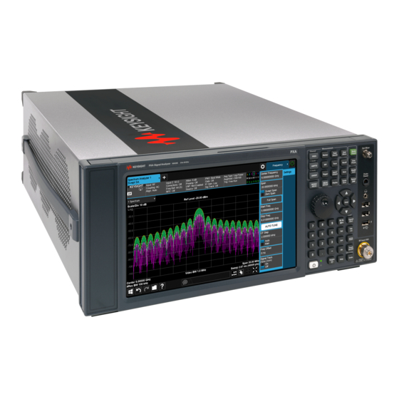
N9030B PXA Signal Analyzer
N9030B Option 503 (3 Hz – 3.6 GHz)
N9030B Option 508 (3 Hz – 8.4 GHz)
N9030B Option 513 (3 Hz – 13.6 GHz)
N9030B Option 526 (3 Hz – 26.5 GHz)
N9030B Option 544 (3 Hz – 44 GHz)
N9030B Option 550 (3 Hz – 50 GHz)
Notice: This document contains references to Agilent.
Please note that Agilent's Test and Measurement
business has become Keysight Technologies. For
more information, go to www.keysight.com.
Service Guide
Advertisement
Chapters
Table of Contents
Troubleshooting

Related Manuals for Keysight Technologies N9030B


Summary of Contents for Keysight Technologies N9030B
- Page 1 Keysight Technologies N9030B PXA Signal Analyzer N9030B Option 503 (3 Hz – 3.6 GHz) N9030B Option 508 (3 Hz – 8.4 GHz) N9030B Option 513 (3 Hz – 13.6 GHz) N9030B Option 526 (3 Hz – 26.5 GHz) N9030B Option 544 (3 Hz – 44 GHz) N9030B Option 550 (3 Hz –...
- Page 2 DOCUMENT OR ANY provided to the public to use, INFORMATION CONTAINED modify, reproduce, release, © Keysight Technologies, Inc. HEREIN. SHOULD KEYSIGHT AND perform, display, or disclose 2016- 2017 THE USER HAVE A SEPARATE commercial computer software or...
- Page 3 Where to Find the Latest Information Documentation is updated periodically. For the latest information about this instrument, including firmware upgrades, application information, and product information, click the website link below. http://www.keysight.com/find/pxa To receive the latest updates by email, subscribe to Keysight Email Updates at the following URL: http://www.keysight.com/find/MyKeysight Information on preventing analyzer damage can be found at: www.keysight.com/find/PreventingInstrumentRepair...
-
Page 5: Table Of Contents
Contacting Keysight Technologies ........ - Page 6 Condition Errors 401 to 499, Power ............141 N9030B PXA Signal Analyzer Service Guide...
- Page 7 Verifying Microwave Preselector Bypass Switch (Option MPB) ........217 N9030B PXA Signal Analyzer Service Guide...
- Page 8 CPU Battery................279 N9030B PXA Signal Analyzer Service Guide...
- Page 9 A26 Wideband Digital IF Troubleshooting - Option B1X and B85 ........329 N9030B PXA Signal Analyzer Service Guide...
- Page 10 Hardware................. . 397 N9030B PXA Signal Analyzer Service Guide...
- Page 11 Rear Panel ................. 510 N9030B PXA Signal Analyzer Service Guide...
- Page 12 Frequency Readout Accuracy..............580 N9030B PXA Signal Analyzer Service Guide...
- Page 13 89600 VSA Software ..............611 N9030B PXA Signal Analyzer Service Guide...
- Page 14 Contents N9030B PXA Signal Analyzer Service Guide...
-
Page 15: Overview
Before You Start Troubleshooting on page 23 ESD Information on page 25 Service Equipment You Will Need on page 29 Required Test Equipment List on page 32 Contacting Keysight Technologies on page 45 How to Return Your Instrument for Service on page 49... -
Page 16: Keysight Pxa Signal Analyzer Overview
Hardware upgrades may require installation of optional hardware, and often require readjustment and verification of the hardware option. Virus Information Keysight Technologies does not load anti-virus software into the signal analyzer. It is the customer’s responsibility to install anti-virus software. N9030B PXA Signal Analyzer Service Guide... -
Page 17: Instrument Option Descriptions
From the front panel, press System, Show System to view a list of all installed options. A current list of all instrument options and retrofit requirements is available on the Keysight web site for the PXA signal analyzer. N9030B PXA Signal Analyzer Service Guide... - Page 18 Included on all units starting August 2013 IM Nulling Included on all units Precision Frequency Reference Included on all units Preamp, 100 kHz to 3.6 GHz Preamp, 100 kHz to 8.4 GHz Preamp, 100 kHz to 13.6 GHz N9030B PXA Signal Analyzer Service Guide...
- Page 19 Preamp, 100 kHz to 26.5 GHz Preamplifier, 44 GHz With Option 544 only Preamplifier, 50 GHz With Option 550 only RT1 or Real Time Analysis Requires option B1X or B85 Screen Video (rear panel Analog Out connector) N9030B PXA Signal Analyzer Service Guide...
-
Page 20: Signal Analyzer Accessories
Signal Analyzer Accessories Signal Analyzer Accessories A number of accessories are available from Keysight Technologies to help you configure your analyzer for your specific applications. They can be ordered through your local Keysight Sales and Service Office and are listed below. -
Page 21: 50 Ohm Load
AC Probe (Low Frequency) The Keysight 41800A low frequency probe has a low input capacitance and a frequency range of 5 Hz to 500 MHz. N9030B PXA Signal Analyzer Service Guide... -
Page 22: Broadband Preamplifiers And Power Amplifiers
Wrist-strap, color black, stainless steel. Four adjustable links and a 7 mm post-type connection. 9300-0980 Wrist-strap cord 1.5 m (5 ft.) 9300-0797 2 ft by 4 ft conductive mat with 15 ft grounding wire N9030B PXA Signal Analyzer Service Guide... -
Page 23: Before You Start Troubleshooting
Any interruption of the protective conductor inside or outside of the product is likely to make the product dangerous. Intentional interruption is prohibited. N9030B PXA Signal Analyzer Service Guide... -
Page 24: Lithium Battery Disposal
The Keysight part number is 1819-1069. The manufacturer’s part number is CR2032. You can return the battery to your nearest Keysight Technologies Sales and Service office for disposal, if required. Refer to “Contacting Keysight Technologies” on page 45 for a list of Keysight Technologies Sales and Service offices. -
Page 25: Esd Information
1 megohm of isolation from ground. These techniques for a static-safe workstation should not be used when working on circuitry with a voltage potential greater than 500 volts. Figure 1-1 Example of a Static-Safe Workstation N9030B PXA Signal Analyzer Service Guide... -
Page 26: Handling Of Electronic Components And Esd
For Additional Information about ESD For more information about preventing ESD damage, contact the Electrical Over Stress/Electrostatic Discharge (EOS/ESD) Association, Inc. The ESD standards developed by this agency are sanctioned by the American National Standards Institute (ANSI). N9030B PXA Signal Analyzer Service Guide... -
Page 27: Instrument Maintenance
Wash thoroughly after handling. In case of spill, soak up with sand or earth. Flush spill area with water. Dispose of isopropyl alcohol in accordance with all applicable federal, state, and local environmental regulations. N9030B PXA Signal Analyzer Service Guide... -
Page 28: Battery Information
Danger of explosion if battery is incorrectly replaced. Replace only with the same or equivalent type recommended. Discard used batteries according to the manufacturer’s instructions. Do not throw batteries away but collect as small chemical waste. N9030B PXA Signal Analyzer Service Guide... -
Page 29: Service Equipment You Will Need
1/4 inch socket on 4 lb torque wrench source locally cable puller 5021-6773 Calibration Application Software Information regarding the Keysight X-Series Signal Analyzer Calibration Application Software can be found at the following web site: www.keysight.com/find/calibrationsoftware N9030B PXA Signal Analyzer Service Guide... -
Page 30: Front End Controller Troubleshooting Kit
E4410-60157 Part of N9020-60005 Troubleshooting kit Cable, Troubleshooting 8121-1400 Right-angle sma (m) to right-angle mmcx (m) (must be ordered separately) Connector, MMCX (f) to SMA (f) www.hubersuhner.com item number: 31_MMCX-SMZ-50-1/111_OE (must be ordered separately) N9030B PXA Signal Analyzer Service Guide... -
Page 31: Usb Keyboard And Mouse
The main reason why a USB storage device will be needed is to download instrument software and backup calibration data when the hard drive in an instrument needs to be replaced. The instrument software is about 1 GB. The calibration files are around 30 megabytes. N9030B PXA Signal Analyzer Service Guide... -
Page 32: Required Test Equipment List
008), VSWR: < 20 GHz: 1.6:1 Response 83640A/B/L ≤ 31 GHz: 1.8:1 Adjustments) (Option 001, 008), 83650A/B/L (Option 001, 008), Performance Tests: 83630A/B (Option 001, 008), 83640A/B (Option 001, 008), 83650A/B (Option 001, 008) N9030B PXA Signal Analyzer Service Guide... - Page 33 Ultra Low Noise Phase Noise) 1 kHz: −132 dBc/Hz Reference Frequency 10 kHz: −144 dBc/Hz Source 30 kHz: −146 dBc/Hz Model 500-13438 100 kHz: −148 dBc/Hz Rev D 1 MHz: −157 dBc/Hz 10 MHz: −164 dBc/Hz N9030B PXA Signal Analyzer Service Guide...
- Page 34 1 MHz to 2 GHz: ≤ 1.10:1 measurement 2 GHz to 3 GHz: ≤ 1.30:1 uncertainty) Cal Factor Uncertainty (std): < 1.6% Option H84 Cal Factor: Characterized by standards lab to: ± 0.6% Input Connector: Type-N (m) N9030B PXA Signal Analyzer Service Guide...
- Page 35 4 GHz to 12.4 GHz: 1.20:11 2.4 GHz to 18 GHz: 1.29:1 18 GHz to 34 GHz: 1.37:1 34 GHz to 40 GHz: 1.61:1 40 GHz to 50 GHz: 1.89:1 Input Connector: 2.4 mm (m) N9030B PXA Signal Analyzer Service Guide...
- Page 36 Characterized by standards lab VSWR: at 50 MHz: ≤ 1.05:1 Attenuator Type N connector kit to connect 8496G 11716A Interconnect Kit to 8494G Attenuator Driver Compatible with the 8496G and 8494G 11713B 11713A step attenuators. N9030B PXA Signal Analyzer Service Guide...
- Page 37 (Option 012) 2.4 mm (f) 50 W 85138B (for Options > 526) Frequency: 10 kHz to 50 GHz 3.5 mm (f) 50 W 909D (for Option 526) Frequency: 10 kHz to 50 GHz (Option 526) N9030B PXA Signal Analyzer Service Guide...
- Page 38 11636B VSWR: < 1.10:1 Tracking Error: <± 0.25 dB Connector: 3.5 mm (f) Hybrid Power Divider Frequency: 500 MHz to 3.6 GHz 87302C Isolation: 19 dB Insertion Loss: 4.5 dB (nominal) VSWR: < 1.45:1 N9030B PXA Signal Analyzer Service Guide...
- Page 39 0955-0491 (2 Required) Rejection at 2.1 GHz to 6 GHz: > 45 dB Insertion Loss at 1.8 GHz: < 1 dB VSWR: ≤ 1.50:1, DC to 1.8 GHz Connector: SMA (f) to SMA (f) N9030B PXA Signal Analyzer Service Guide...
- Page 40 Type-N (f) to 3.5 mm (m) Frequency: DC to 18 GHz 1250-1750 VSWR: ≤ 1.14:1 3.5 mm (f) to 3.5 mm (f) Frequency: DC to 26.5 GHz 83059B 1250-1749 (for 3.5 mm source) VSWR: ≤ 1.05:1 N9030B PXA Signal Analyzer Service Guide...
- Page 41 E8257D E8267C E8267D Note: One PSG with Option 567, 1EA/1EU, 1E1, 007, and UNX or UNR can be used as the Microwave Signal Generator #1, Low Noise Signal Generator, and the RF Signal Generator. N9030B PXA Signal Analyzer Service Guide...
- Page 42 The step attenuator combination should have each attenuator setting characterized by a metrology lab at 50 MHz. This characterization can be ordered through Keysight Technologies as an Option H50 Calibration. The following tables show which sections of the 10 dB and 1 dB step attenuators are utilized for each attenuator setting.
- Page 43 (dB) (dB) (10 dB) (20 dB) (40 dB) (40 dB) 0 (Reference) < 0.010 < 0.015 < 0.020 < 0.025 < 0.030 < 0.035 < 0.040 a. TME requires that Section 3 be characterized. N9030B PXA Signal Analyzer Service Guide...
-
Page 44: After An Instrument Repair
Chapter 17, “Post-Repair Procedures” for a list of post-repair adjustments and performance tests based on which hardware has been changed. Information regarding the N7814A Keysight X-Series Signal Analyzer Calibration Application Software can be found at http://www.keysight.com/find/calibrationsoftware N9030B PXA Signal Analyzer Service Guide... -
Page 45: Contacting Keysight Technologies
Keysight office listed in Table 1-4. In any correspondence or telephone conversations, refer to the instrument by its model number (N9030B) and full serial number (ex. MY49250887). With this information, the Keysight representative can quickly determine whether your unit is still within its warranty period. - Page 46 (65) 6375 8100 Europe and Middle Country Phone Number Austria 0800 001122 Belgium 0800 58580 Finland 0800 523252 France 0805 980333 Germany 0800 6270999 Ireland 1800 832700 Israel 1 809 343051 Italy 800 599100 N9030B PXA Signal Analyzer Service Guide...
- Page 47 +32 800 58580 Netherlands 0800 0233200 Russia 8800 5009286 Spain 0800 000154 Sweden 0200 882255 Switzerland 0800 805353 Opt. 1 (DE) Opt. 2 (FR) Opt. 3 (IT) United Kingdom 0800 0260637 For other unlisted countries: www.keysight.com/find/contactus N9030B PXA Signal Analyzer Service Guide...
-
Page 48: Instrument Serial Numbers
The serial number is located on the rear panel serial sticker or when the analyzer is power up, press System, Show System. The system information can be very useful for updates and post-sale upgrades. N9030B PXA Signal Analyzer Service Guide... -
Page 49: How To Return Your Instrument For Service
Original Packaging Before shipping, pack the unit in the original factory packaging materials if they are available. If the original materials were not retained, see “Other Packaging” on page N9030B PXA Signal Analyzer Service Guide... -
Page 50: Other Packaging
5. Seal the shipping container securely with strong nylon adhesive tape. 6. Mark the shipping container “FRAGILE, HANDLE WITH CARE” to assure careful handling. 7. Retain copies of all shipping papers. N9030B PXA Signal Analyzer Service Guide... -
Page 51: Boot Up And Initialization Troubleshooting
Keysight Technologies N9030B PXA Signal Analyzer Service Guide Boot Up and Initialization Troubleshooting What You Will Find in This Chapter This chapter provides information that is useful when starting to troubleshoot a spectrum analyzer. It includes procedures for troubleshooting common failures and provides information on isolating problems in the analyzer. -
Page 52: Check The Basics
Boot Up and Initialization Troubleshooting Check the Basics Check the Basics Before calling Keysight Technologies or returning the instrument for service, please make the following checks: 1. Is there power at the power outlet? At the power receptacle on the instrument? 2. -
Page 53: Pxa Instrument Boot Up Process
PXA Instrument Boot Up Process PXA Instrument Boot Up Process This section describes the N9030B Signal Analyzer boot up process from initial AC power to a normal analyzer sweep. The boot process time from start to finish will take 6 to 8 minutes. This boot time will vary slightly depending on the analyzer hardware configuration, installed options and the number of measurement applications. -
Page 54: Typical Instrument Boot-Up Process Flow
On/Off button on the front panel. N9030B PXA Signal Analyzer Service Guide... - Page 55 Operating” section in this chapter. 5. The Keysight Technologies splash screen is displayed in white font on a dark background for ~5-10 seconds after the analyzer is turned on. If the Keysight Technologies logo is not displayed refer to the “No Keysight...
- Page 56 If the power up state has been changed from the factory power on state by IMPORTANT the user, the analyzer will boot to that state. Figure 2-2 Typical Instrument Sweep at Power-up (Display theme changed for printing clarity) N9030B PXA Signal Analyzer Service Guide...
-
Page 57: Potential Problems During Boot Process
2. Remove the AC power cord and then remove the instrument cover. Refer Chapter 16, “Assembly Replacement Procedures”, on page 429 in this manual. 3. Referring to Figure 2-3, verify the +5.1VSB LED on the A7 Midplane board is on (green). N9030B PXA Signal Analyzer Service Guide... - Page 58 LED back to the A4 Processor board are not at fault, replace the A4 Processor board. If not: Replace the A6 Power Supply assembly. Before replacing the power supply, verify the midplane and motherboard interconnects are mechanically secure. N9030B PXA Signal Analyzer Service Guide...
-
Page 59: Green Power On Led Does Not Illuminate
Does the voltage at Test Point 518 measure 5 VDC? If yes: Proceed to step If not: Replace the A6 Power Supply assembly. Before replacing the power supply, verify the midplane and motherboard interconnects are mechanically secure. N9030B PXA Signal Analyzer Service Guide... - Page 60 TTL low level. The A4 Processor board assembly provides the voltage and the switch on the front panel pulls it low when it is pressed. N9030B PXA Signal Analyzer Service Guide...
- Page 61 7. To verify that the A6 Power Supply is not in an over current condition, check the status of the FAULT_L status line by measuring the voltage level at Test Point 508 or viewing the FAULT_L LED, as shown in Figure 2-6. N9030B PXA Signal Analyzer Service Guide...
- Page 62 If no assembly can be found that is causing the overcurrent condition, replace the A6 Power Supply assembly. Figure 2-6 A7 Midplane Board - Test Point 508/FAULT_L LED Before replacing the power supply, verify the midplane and motherboard interconnects are mechanically secure. N9030B PXA Signal Analyzer Service Guide...
-
Page 63: Fan(S) Are Not Operating
3. Are all three fans not spinning? If yes: Proceed to step If not: Proceed to step 4. Remove the Top Brace. Refer to Chapter 16, “Assembly Replacement Procedures”, on page 429 in this manual. N9030B PXA Signal Analyzer Service Guide... - Page 64 If not: Replace the A6 Power Supply assembly. Before replacing the power supply, verify the midplane and motherboard interconnects are mechanically secure. Figure 2-7 A7 Midplane Board - Fan_P Failure LED / Test Point 522 N9030B PXA Signal Analyzer Service Guide...
-
Page 65: No Keysight Splash Screen Displayed
A8 Motherboard. No Keysight Splash Screen Displayed (Black background with white “Keysight Technologies” text) A problem of not displaying the Keysight splash screen could be caused by many different things. It could be due to a down power supply, a processor hardware problem, an instrument boot-up process error, a display section failure, etc. - Page 66 4. Connect an external VGA monitor to the rear panel display output. Does the external monitor display the correct information? If yes: Proceed to the “Troubleshooting a Blank Display” section in this chapter. If not: Replace the A4 Processor Board assembly. N9030B PXA Signal Analyzer Service Guide...
-
Page 67: Instrument Hangs At The Keysight Splash Screen
A4 Processor board are not at fault, replace the A4 Processor board. If not: After verifying that the connections between the A6 Power Supply, the A7 Midplane board, and the A8 Motherboard are all mechanically and electrically secure, replace the A6 Power Supply assembly. N9030B PXA Signal Analyzer Service Guide... -
Page 68: Instrument Cannot Completely Load Or Run The Operating System
They are: — An LCD Backlight inverter problem — A video signal path integrity problem — A video controller / LCD problem N9030B PXA Signal Analyzer Service Guide... -
Page 69: Verify Lcd Backlight Functionality
5. Can the expected display information now be seen? If yes: The problem is backlight related. Proceed to step If not: The problem is not backlight related. Skip to “Verify Video Signal Path Integrity”. N9030B PXA Signal Analyzer Service Guide... - Page 70 “Inverter Enable” voltage measures too low, press a front panel key and see if the voltage level increases to the expected level. N9030B PXA Signal Analyzer Service Guide...
- Page 71 >6 VDC Inverter Supply +12 VDC 10.Are all of the 3 voltage levels within their expected ranges? If yes: Replace the A1A4 LCD Inverter board. If not: Replace the A1A2 Front Panel Interface board. N9030B PXA Signal Analyzer Service Guide...
-
Page 72: Verify Video Signal Path Integrity
Start, Run, enter Eventvwr.exe, and select OK. Once the Event Viewer comes up, look under SA for the latest error entries. Double-click on the entries to view further details, which should give you some idea of what the problem is. N9030B PXA Signal Analyzer Service Guide... -
Page 73: Fails An Initial Alignment
Assure there is no 50 MHz signal above 0 dBm applied to the signal analyzer input when the alignment routine is performed. This can cause errors. The description of the alignment and the alignment hardware dependencies are listed in Table 2-3. N9030B PXA Signal Analyzer Service Guide... - Page 74 Algorithm Adjusts the LC prefilter centering with the prefilter BW set to about 1.12 MHz. Uses 322.5 MHz Comb Calibrator on the A-IF. AIF LC Wide Prefilter Passband Fine Tuning A2 Analog IF Algorithm N9030B PXA Signal Analyzer Service Guide...
- Page 75 “Swept IF Gain”. Uses the Comb calibrator on the A-IF LO Power Alignment Algorithm A13 Front End Measure max LO power then backs off for each Assembly or A15 band Front End Controller N9030B PXA Signal Analyzer Service Guide...
- Page 76 MB = medium bandwidth LO Nulling Min MB Alignment Algorithm A13 Front End LO Nulling Full WB Alignment Algorithm A13 Front End WB = Wide Band (Option B1X) LO Nulling Min WB Alignment Algorithm A13 Front End N9030B PXA Signal Analyzer Service Guide...
- Page 77 Analog IF is not included in the signal path. DIF 40 Step Cal Alignment Algorithm AIF 140 Step Cal Ad justment Alignment A25 Wide band A-IF Algorithm (Option B1X) AIF 140 Step Cal Alignment Algorithm N9030B PXA Signal Analyzer Service Guide...
- Page 78 Aligns low band (3 Hz to 3.6 GHz path) with A9 and A10 Input preamp and electronic attenuator OFF. attenuators Dependent on successful E-Cal alignment. Input attenuators set to 10 dB and DC coupled. N9030B PXA Signal Analyzer Service Guide...
- Page 79 4800 MHz calibrator on A16 A12 YTF Preselector is bypassed and amplitude Reference of 4800 MHz calibrator measured. System gain is then computed. (Option MPB) A9 and A10 Input attenuators N9030B PXA Signal Analyzer Service Guide...
- Page 80 E:\AlignDataStorage\AlignmentHistory.txt You will find the most current alignment information at the bottom of this file. Look for the failed alignments and troubleshoot the Related Hardware based on the information provided in Table 2-3. N9030B PXA Signal Analyzer Service Guide...
-
Page 81: Signal Level Verification
It is possible that other input frequencies < 3.6 GHz could have an amplitude problem even though the 50 MHz calibrator is within tolerance. Using the internal RF calibrator provides a quick check of the low band path. N9030B PXA Signal Analyzer Service Guide... -
Page 82: Signal Level Problem With Input Frequencies > 3.6 Ghz
It is possible that other input frequencies > 3.6 GHz could have an amplitude problem even though the 4.8 GHz calibrator is within tolerance. Using the internal RF calibrator provides a quick check of the high band path. N9030B PXA Signal Analyzer Service Guide... -
Page 83: Instrument Messages
Keysight Technologies N9030B PXA Signal Analyzer Service Guide Instrument Messages Introduction The Error and Status messaging system of the Keysight Signal Analyzer reports events and conditions in a consistent fashion, as well as logging and reporting event history. Event vs. Condition Messages An Event is simply a message indicating that something has happened. -
Page 84: Event And Condition Categories
Warnings are logged in the error queues. If the warning is a condition, both the Detected and Cleared event messages are logged. N9030B PXA Signal Analyzer Service Guide... -
Page 85: Event Message Format
IEEE Standard 488.2-1992, IEEE Standard Codes, Formats, Protocols and Common Commands for Use with ANSI / IEEE Std 488.1-1987. New York, NY, 1992. N9030B PXA Signal Analyzer Service Guide... -
Page 86: Event Queues
Circular (rotating). Circular (rotating). Linear, first-in/first-out. Overflow Handling Drops oldest error as new Drops oldest error as new Replaces newest error with: error comes in. error comes in. −350, Queue overflow N9030B PXA Signal Analyzer Service Guide... - Page 87 Displayed in Message Line Grayout Advisory (Forced) Logged Displayed in Message Line See note a. Not logged, unless the cause of the Advisory was remotely generated, in which case a Warning mes- sage, type –221, is logged. N9030B PXA Signal Analyzer Service Guide...
-
Page 88: Advisory Messages
If Marker Function is off changing the band has no effect Band Adjust has no effect with Mkr Function Off Turning on any high-pass or low-pass filter will turn off band pass filters. Band-pass filter set to OFF N9030B PXA Signal Analyzer Service Guide... - Page 89 Use the graph icon on the DUT setup form to clarify the setup required. Logarithmic scaling cannot be used for time domain sweeps Freq Scale Type=Log is not (0 Hz span). available in Zero Span N9030B PXA Signal Analyzer Service Guide...
- Page 90 The LO fixed freq should be greater than the IF Stop freq for an LSB upconverter fixed LO setup. Use the graph icon on the DUT setup form to clarify the setup required. N9030B PXA Signal Analyzer Service Guide...
- Page 91 The latest cable calibration data will be used cal; using cable cal data; <port>; <probe> A probe has been disconnected, calibration data reverting to the last cable Probe disconnected, calibration data reverting to cable calibration data; <port> N9030B PXA Signal Analyzer Service Guide...
- Page 92 Signal Track is turned off Span is entered while in Signal Track is On, Signal Track is turned off. when Zero Span is selected The signals in the signal list were successfully deleted. Signals deleted N9030B PXA Signal Analyzer Service Guide...
- Page 93 The measurement setup has changed such that the current cal data can be User Cal valid. Apply Cal applied to the results. To apply the cal, press Meas Setup/Cal Setup/Apply from Meas Setup menu Calibration. A new cal can be performed if required. N9030B PXA Signal Analyzer Service Guide...
-
Page 94: Event Messages
–221 is defined as “Settings Conflict”, but in the X-Series you will often see a longer message with error –221, such as “Settings Conflict; Function not available in Zero Span”. This helps you understand exactly why you are getting a Settings Conflict error. N9030B PXA Signal Analyzer Service Guide... -
Page 95: 800, Operation Complete Event
Some condition caused a DEADLOCKED query to occur. For Query DEADLOCKED example, both the input buffer and the output buffer are full and the analyzer cannot continue. The analyzer automatically discards output to correct the deadlock. N9030B PXA Signal Analyzer Service Guide... -
Page 96: -300 To -399, Device-Specific Errors
Verbose/Correction Information –300 An instrument error occurred and the exact problem cannot be specifically Device-specific error identified. Report this error to the nearest Keysight Technologies sales or service office. –310 An internal system-type error has occurred. The exact problem cannot be System error;... - Page 97 System error; The Trigger alarm was not scheduled due to a conflict with an existing scheduled alarm. –311 There is a physical problem with the instrument memory, such as a parity Memory error error. N9030B PXA Signal Analyzer Service Guide...
- Page 98 –321 An internal operation needed more memory than was available. Report this Out of memory error to the nearest Keysight Technologies sales or service office. –330 A self-test failure occurred. Report this error to the nearest Keysight Self-test failed Technologies sales or service office.
-
Page 99: -221 Settings Conflict Errors
User Cal is required. cal first or apply existing cal. Optimize aborted –221 The Auto Tune feature cannot be used when you are using a Settings conflict; Auto Tune Tracking Source. not available in Tracking Source mode N9030B PXA Signal Analyzer Service Guide... - Page 100 Continuous Peak is not available with Fixed marker –221 The continuous peak feature cannot be used while you are Settings conflict; also using the signal tracking function. Continuous Peak is not available with Signal Track N9030B PXA Signal Analyzer Service Guide...
- Page 101 –221 This functionality is not a part of the instrument you are Settings conflict; Feature using but may be found in other models in the X-Series. not supported for this model number N9030B PXA Signal Analyzer Service Guide...
- Page 102 Edge for Gated –221 You cannot use level triggering to control the gate when you Settings conflict; Gate are using the currently selected gate source. control must be Edge for this Gate Source N9030B PXA Signal Analyzer Service Guide...
- Page 103 –221 For instruments without the Dual-Loop LO, this feature is not Settings conflict; LO Phase available Noise Adj not available N9030B PXA Signal Analyzer Service Guide...
- Page 104 –221 Mobile Station gain correction is not available in some Settings conflict; MS gain Modes, or in some measurements (for example, the SA is not available in this measurement). Mode N9030B PXA Signal Analyzer Service Guide...
- Page 105 LO Mode is Fixed –221 SCPI only message. This parameter is only available when Settings conflict; Param the Freq mode is set to Fixed. Change the Freq Mode to only available when Fixed. Frequency Mode is Fixed N9030B PXA Signal Analyzer Service Guide...
- Page 106 Span. So if Zero Span is entered while in Signal Track is On, Track is turned off when Signal Track is turned off. Zero Span is selected –221 Settings Conflict; Span limited to XXX N9030B PXA Signal Analyzer Service Guide...
- Page 107 If using an SNS the Tcold value may be read automatically before every sweep. –221 Settings Conflict; The parameter cannot be changed in FAST mode N9030B PXA Signal Analyzer Service Guide...
- Page 108 They are always mutually exclusive. Detectors and Average detector can’t be used together –221 Frequency is limited to 1GHz while RF Input 2 is enabled. Settings conflict;Freq > 1 GHz is not available while RF Input 2 enabled N9030B PXA Signal Analyzer Service Guide...
- Page 109 Step/Time Control. –221 The Step Size & Meas Time are not available when Settings conflict;Step Size Step/Time Control is set to Scan Time&Pts. & Meas Time do not apply in current Step/Time Control. N9030B PXA Signal Analyzer Service Guide...
-
Page 110: -200 To -299, Execution Errors
Execution Error; No peak search. found. –200 There are no active ranges in the range table. You will need to Execution error; No ranges activate at least one range. are defined. Activate a range. N9030B PXA Signal Analyzer Service Guide... - Page 111 Please clear the list. –200 The signal selected is not the list. You only can perform the Signal Selected is not in operation on signal that is already available in the list. the Signal List N9030B PXA Signal Analyzer Service Guide...
- Page 112 –222 You tried to use a trace that has a number of sweep points that is Data out of range; Invalid different from the current setting of sweep points. list data N9030B PXA Signal Analyzer Service Guide...
- Page 113 When querying the LXI Event Log or the Servo Log, an index may Illegal parameter value; be used to look at a specific entry. This error occurs if the index Index out of range provided does not point to a valid entry. N9030B PXA Signal Analyzer Service Guide...
- Page 114 Trace cannot be displayed because currently there is no data Data corrupt or stale; assigned to it. Use the functions under the Trace menu, or load a Trace contains no data. previously saved trace, to assign data to the trace. N9030B PXA Signal Analyzer Service Guide...
- Page 115 Trace files containing multiple traces can not be imported. Mass storage error; Can However, if you need to recall multiple traces you can use the only import single trace Save and Recall functions rather than the Import and Export .csv files functions. N9030B PXA Signal Analyzer Service Guide...
- Page 116 The system cannot open the device or file specified. This could be Mass storage error; Open because the storage media is full, or possibly due to a filename failed error. If using an external storage devise, check that the devise is properly formatted. N9030B PXA Signal Analyzer Service Guide...
- Page 117 You are using the wrong type of file extension for the current File name error; Allowable data/file type. extension is .state –257 The filename, directory name, or volume label syntax is incorrect. File name error; Invalid file name –257 File name error; name too long N9030B PXA Signal Analyzer Service Guide...
- Page 118 An attempt was made to reference a nonexistent variable in a Illegal variable name program. –284 Certain operations dealing with programs may be illegal while the Program currently running program is running; for example, deleting a running program might not be possible. N9030B PXA Signal Analyzer Service Guide...
- Page 119 –290 Memory use errors –291 Out of memory –292 Referenced name does not exist –293 Referenced name already exists –294 Indicates that the type or structure of a memory item is Incompatible type inadequate N9030B PXA Signal Analyzer Service Guide...
-
Page 120: -100 To -199, Command Errors
A character was found that is not valid for the data type. For Invalid character in example, an alpha in a decimal numeric or a “9” in octal data. number –123 The magnitude of an exponent was greater than 32000. Exponent too large N9030B PXA Signal Analyzer Service Guide... - Page 121 A problem was found with an expression data element. The exact Expression error problem cannot be specifically identified. –171 An expression data element is not valid. For example, there may Invalid expression be unmatched parentheses or an illegal character. N9030B PXA Signal Analyzer Service Guide...
-
Page 122: Error
0 Error Err# Message Verbose/Correction Information The queue is empty. Either every error in the queue has been No error read, or the queue was cleared by power-on or *CLS. N9030B PXA Signal Analyzer Service Guide... -
Page 123: Condition Messages
See section “Condition Errors 36 to 64, Calibration Needed or Failed” on page 124. Err# Bit in Message Error or More Information status Warning register Align RF Skipped unused unused unused unused unused N9030B PXA Signal Analyzer Service Guide... - Page 124 PTRansition filter set, or a true-to-false transition with the NTRansition filter set, in any of the :CALibration sub-registers :SKIPped, :EXTended:NEEDed or :EXTended:FAILure. N9030B PXA Signal Analyzer Service Guide...
- Page 125 This bit is the summary bit for the Align Skipped Sum Summary only STATus:QUEStionable:CALibration:SKIPped sub-register. Align Now, RF required unused On PSA, this was error 64 Align Now, All required N9030B PXA Signal Analyzer Service Guide...
- Page 126 Corrected measurements have been Input Attenuation not requested and the required RF calibrated front-end setting of x dB has not been calibrated. unused unused unused unused unused unused unused unused unused unused N9030B PXA Signal Analyzer Service Guide...
- Page 127 Align 9kHz to 30MHz failed On PSA, this was error 13751 Align 30MHz to 1GHz failed The preselector characterization routine Characterize Preselector failed. failure unused unused unused unused unused unused unused unused unused unused unused unused N9030B PXA Signal Analyzer Service Guide...
-
Page 128: Condition Errors 101 To 199, Measurement Integrity
No Result To calculate Timing and Phase results in No Result;Turn on MCE the Code Domain Power view of Mod Accuracy, the “Multi Channel Estimator” must be set to ON. Otherwise these results are invalid. N9030B PXA Signal Analyzer Service Guide... - Page 129 ENR table (Common, Meas or Cal). A measurement is attempted or a SCPI Insufficient Data; Loss query of a before or after loss table is table empty made and there are no entries in the relevant loss table N9030B PXA Signal Analyzer Service Guide...
- Page 130 Increase the AF Spectrum RBW or the RF Spectrum RBW, decrease the Channel BW, and/or decrease the Demod Waveform Sweep Time. N9030B PXA Signal Analyzer Service Guide...
- Page 131 For Bluetooth, the detected Settings Alert;Parm/data parameters did not match the data mismatch Setting Modified The filter you have selected is larger Setting Modified; Filter not than the sampling frequency. You applied should select a different filter. N9030B PXA Signal Analyzer Service Guide...
-
Page 132: Condition Errors 201 To 299, Signal Integrity
This register is summarized as bit 0 of the STATus:QUEStionable:INTegrity register. See section “Condition Errors 101 to 199, Measurement Integrity” on page 128. Err# Bit in Message Error or More Information Status Warning Register unused unused N9030B PXA Signal Analyzer Service Guide... - Page 133 In the PSA, this error was reported as one of the following error numbers: 10772, 13104, 10160, 10286, 10420, 10454, 10614, 10904, 10928, 13074, 10287 The selected timeslot does not contain the Burst not found;with expected burst. selected Time Slot N9030B PXA Signal Analyzer Service Guide...
- Page 134 Failed to find the uplink slot, which caused the Sync Error;Midamble synchronization with the midamble to fail. sync fail Burst type is “Data” or “Preamble” and the Sync Error;Preamble measurement cannot find a Preamble length zero N9030B PXA Signal Analyzer Service Guide...
- Page 135 There are not enough input I/Q pairs for the Demod Error;Data measurement calculation. This may be caused interval too short by an incorrect data capture. There is no active channel detected. Demod Error;No active channel N9030B PXA Signal Analyzer Service Guide...
- Page 136 Slot Error; No idle idle slot found in captured interval. slot found Synchronization may succeed and pilot found when this message is issued, but no results are included in peak/average calculation. unused unused unused unused unused N9030B PXA Signal Analyzer Service Guide...
-
Page 137: Condition Errors 301 To 399, Uncalibrated Integrity
Meas Uncal Signal ID on No Long Code Phase AC input coupling will function at lower AC coupled: Accy unspec’d frequencies, but the performance is not <10 MHz specified below 10 MHz. User cal N9030B PXA Signal Analyzer Service Guide... - Page 138 A successful calibration has been performed. • Some measured freq points are > 3.6 GHz. • The new points > 3.6 GHz are located more than 50 MHz away from the current calibration points. N9030B PXA Signal Analyzer Service Guide...
- Page 139 LO feedthrough in the trace. This depends on both Start Freq and RBW. If you get this message, increase your Start Freq or narrow your RBW. unused unused unused unused unused unused unused N9030B PXA Signal Analyzer Service Guide...
- Page 140 Instrument Messages Condition Messages Err# Status Message Error or Verbose/Correction Information Register Warning unused N9030B PXA Signal Analyzer Service Guide...
-
Page 141: Condition Errors 401 To 499, Power
(not currently in use) RPP Tripped Source Unleveled (not currently in use) Source LO Unleveled (not currently in use) LO Unleveled unused unused unused unused unused Preselector Overload unused unused unused unused unused N9030B PXA Signal Analyzer Service Guide... -
Page 142: Condition Errors 501 To 599, Frequency
The external frequency reference signal External ref missing or is missing or is not within the proper out of range amplitude range. In the PSA, this error was reported as error 622 unused unused unused unused N9030B PXA Signal Analyzer Service Guide... -
Page 143: Condition Errors 601 To 699, Error Summaries
STATus:QUEStionable:POWer sub-register. status bit This bit is the summary bit for the Temperature only STATus:QUEStionable:TEMPerature sub-register. status bit This bit is the summary bit for the Frequency only STATus:QUEStionable:FREQuency sub-register. Phase unused Modulation unused N9030B PXA Signal Analyzer Service Guide... - Page 144 This bit is the summary bit for the Calibration only STATus:QUEStionable:CALibration sub-register. status bit This bit is the summary bit for the Integrity only STATus:QUEStionable:INTegrity sub-register. unused CALL unused unused unused Command Warning unused N9030B PXA Signal Analyzer Service Guide...
-
Page 145: Condition Errors 701 To 799, Operation
Waiting for Trigger status bit only Waiting for Arm unused status bit only Paused status bit only Source Sweeping DC Coupled unused status bit only Source Waiting for Trigger unused unused N9030B PXA Signal Analyzer Service Guide... -
Page 146: Condition Errors 801 To 899, Temperature
143. Err# Bit in Message Error or More Information status Warning register (not currently in use) Reference Oscillator Oven Cold unused unused unused unused unused unused unused unused unused unused unused unused unused unused N9030B PXA Signal Analyzer Service Guide... -
Page 147: Rf Section Troubleshooting (Rf/Microwave Analyzers)
Keysight Technologies N9030B PXA Signal Analyzer Service Guide RF Section Troubleshooting (RF/Microwave Analyzers) What You Will Find in This Chapter The following information is found in this chapter: 1. Theory of operation of the RF section. 2. Isolating the cause of an hardware problem by verifying the functionality of assemblies in the RF section signal path. -
Page 148: Rf Section Description
140 MHz (Option B1X) 300 MHz IQ Analyzer 160 MHz (Option B1X & B1Y) 300 MHz IQ Analyzer 255 MHz (Option B2X) 750 MHz IQ Analyzer 510 MHz (Option B5X) 877.148 MHz IQ Analyzer N9030B PXA Signal Analyzer Service Guide... - Page 149 4800 MHz (2nd LO)). The 2nd IF output is at A13A1J7. This signal path is used for all frequency range options when the RF input frequencies are < 3600 MHz. The control voltages and biasing for these assemblies come from the A15 Front End Control assembly. N9030B PXA Signal Analyzer Service Guide...
-
Page 150: A9 Input Attenuator A
Low Band Switch assembly. There is a 6 dB, 10 dB, 20 dB, and 30 dB section in the A10 assembly. Total input attenuation with the A9 and the A10 combined is 70 dB in 2 dB steps. N9030B PXA Signal Analyzer Service Guide... -
Page 151: A11 Low Band Switch
The 1st LO has a frequency range from 3.80 to 8.73 GHz. The output power is +13 to +18 dBm. In order to maximize the conversion efficiency and avoid LO unlock, sufficient LO power must be supplied. N9030B PXA Signal Analyzer Service Guide... -
Page 152: A13 Rf Front End Assembly
A13A2 contains the switched filters and LO and IM nulling circuits. A13A1 and A13A2 are not separately replaceable. The entire A13 assembly must be replaced. See Figure 4-1. Figure 4-1 A13 RF Front End Assembly View from Front Panel N9030B PXA Signal Analyzer Service Guide... - Page 153 — Front End Assembly including switched filter — (Optional) High Band Preamplifier — (Optional) Low Band Preamplifier — (Option EA3) Electronic Attenuator (0-24 dB) Refer to Chapter 6, “Front End Control Troubleshooting.” for detailed descriptions & troubleshooting procedures. N9030B PXA Signal Analyzer Service Guide...
-
Page 154: Troubleshooting
To verify the high band path go to “Quick Check to Verify High Band RF Path” on page 163. If the power level is not within tolerance, press SPAN (X Scale), Zero Span, AMPTD (Y Scale), Attenuation, 10 dB. N9030B PXA Signal Analyzer Service Guide... - Page 155 Reconnect the W16 cable to A13A1J7. Flatness issues or power level problems at other input frequencies below 3600 MHz may exist. This type of problem can be diagnosed using an external source to verify performance. N9030B PXA Signal Analyzer Service Guide...
- Page 156 In order to gain access to the front end components, remove the front frame assembly, but leave the ribbon cable connected so you can still control the instrument. Remove the right side chassis. Refer to the removal procedures in Chapter 16, “Assembly Replacement Procedures”. N9030B PXA Signal Analyzer Service Guide...
-
Page 157: Troubleshooting A Low Band Problem
Low Band output at W8 is incorrect, suspect the A11 Low Band Switch, the interconnect cables, Switch 3 if Option LNP is present, or the control signals. The control signals are explained in Chapter 6, “Front End Control Troubleshooting”, on page 199. N9030B PXA Signal Analyzer Service Guide... - Page 158 RF Section Troubleshooting (RF/Microwave Analyzers) Troubleshooting Figure 4-3 RF Section N9030B PXA Signal Analyzer Service Guide...
- Page 159 Both set to through path −2 −4 −6 A9 set to 2 dB, −8 A10 set to 6 dB −10 −20 −30 −40 −50 −60 A9 set to 4 dB, −70 A10 set to 66 dB N9030B PXA Signal Analyzer Service Guide...
- Page 160 The input signal level was measured on W8 as part of the A11 Low Band Switch verification. The output signal level was measured at A13A1J7 during the quick check to verify the Low Band Signal Path. The Second LO input was tested during the Second LO Verification. N9030B PXA Signal Analyzer Service Guide...
- Page 161 Assure you have evaluated all causes before you replace the Front End assembly. If you determine the problem is at a frequency other than 50 MHz, perform the low band flatness adjustment before replacing the Front End assembly. N9030B PXA Signal Analyzer Service Guide...
- Page 162 RF is the input signal at the signal analyzer Low Band second mixer: RF = LO + IF IF = RF − LO LO = RF − IF where RF in this case is the first IF signal (signal at A13A1J11) N9030B PXA Signal Analyzer Service Guide...
-
Page 163: Quick Check To Verify High Band Rf Path
50 MHz. Since several of the same signal path components are shared between high band and low band, determining if the problem appears in both paths is helpful Turn off auto align by pressing System, Alignments, Auto Align, Off. IMPORTANT N9030B PXA Signal Analyzer Service Guide... - Page 164 RF Section Troubleshooting (RF/Microwave Analyzers) Troubleshooting Disconnect cable W16 at A13A1J7, 322.5 MHz output on the Front End Assembly. See Figure 4-4. Select Span, 0 Hz. Figure 4-4 A13A1J7 Location (Options 503, 508, 513, and 526) N9030B PXA Signal Analyzer Service Guide...
- Page 165 1. A11 Low Band Switch 2. A10 Input Attenuator B 3. A9 Input Attenuator A 4. A16 Reference Assembly (4.8 GHz calibrator) 5. A20 YTO 6. A12 YTF Preselector 7. A13 Front End Assembly N9030B PXA Signal Analyzer Service Guide...
- Page 166 A13 RF Front End Assembly. In order to gain access to the front end components, remove the side chassis (1) by removing the 16 screws (2). See Figure 4-6. Figure 4-6 Remove the Side Chassis N9030B PXA Signal Analyzer Service Guide...
-
Page 167: Troubleshooting A High Band Problem
If the signal level is incorrect, and Option MPB (Microwave Preselector Bypass) is installed, press Amplitude, More, uWPath Control, uW Preselector Bypass. If the signal level is now −52 dBm, suspect the A12 YTF is out of adjustment or faulty. N9030B PXA Signal Analyzer Service Guide... - Page 168 On the A16 Reference assembly, disconnect semi rigid cable W3 from A16J701 and measure A16J701 with a spectrum analyzer. Expected signal is 4.8 GHz at −28 dBm ± 0.5 dB. If signal level is incorrect, suspect A16 Reference Assembly. N9030B PXA Signal Analyzer Service Guide...
- Page 169 To assure the first LO is tuned to the correct frequency and power, measure the A13 Front End assembly at A13A1J3 when the analyzer center frequency is 4.8 GHz. This test port is chosen because removing cable W19 will not cause N9030B PXA Signal Analyzer Service Guide...
- Page 170 (using the calibration software) will adjust the preamp on, high band path. Assure you have evaluated all causes including A15 Front End Controller switching problems, before you replace the Front End assembly. N9030B PXA Signal Analyzer Service Guide...
- Page 171 Depending on the signal source connected, you may see many “signals” appear on screen because without preselection, the analyzer will display images and multiples. The real input signal should not change amplitude when you switch the uW Preselector Bypass on and off. N9030B PXA Signal Analyzer Service Guide...
- Page 172 RF Section Troubleshooting (RF/Microwave Analyzers) Troubleshooting N9030B PXA Signal Analyzer Service Guide...
-
Page 173: Rf Section Troubleshooting (Millimeter-Wave Analyzers)
Keysight Technologies N9030B PXA Signal Analyzer Service Guide RF Section Troubleshooting (Millimeter-Wave Analyzers) What You Will Find in This Chapter The following information is found in this chapter: 1. Theory of operation of the RF section. 2. Isolating the cause of an hardware problem by verifying the functionality of assemblies in the RF section signal path. -
Page 174: Rf Section Description
140 MHz (Option B1X) 300 MHz IQ Analyzer 160 MHz (Option B1X & B1Y) 300 MHz IQ Analyzer 255 MHz (Option B2X) 750 MHz IQ Analyzer 510 MHz (Option B5X) 877.148 MHz IQ Analyzer N9030B PXA Signal Analyzer Service Guide... - Page 175 4800 MHz (2nd LO)). The 2nd IF output is at A13A1J7. This signal path is used for all frequency range options when the RF input frequencies are < 3600 MHz. The control voltages and biasing for these assemblies come from the A15 Front End Control assembly. N9030B PXA Signal Analyzer Service Guide...
-
Page 176: A9 Input Attenuator A
The LO is doubled for all tuned frequencies in this path. A9 Input Attenuator A This assembly has two 2 dB attenuator sections, a 6 dB attenuator section, and a cal signal input port. N9030B PXA Signal Analyzer Service Guide... -
Page 177: A10 Input Attenuator B
The 1st LO has a frequency range from 3.80 to 8.73 GHz. The output power is +13 to +18 dBm. In order to maximize the conversion efficiency and avoid LO unlock, sufficient LO power must be supplied. N9030B PXA Signal Analyzer Service Guide... -
Page 178: A13 Rf Front End Assembly (Options 544, 550)
A13A2 contains the switched filters and LO and IM nulling circuits. A13A1 and A13A2 are not separately replaceable. The entire A13 assembly must be replaced. See Figure 5-1. Figure 5-1 A13 RF Front End Assembly View from Front Panel N9030B PXA Signal Analyzer Service Guide... - Page 179 — Front End Assembly including switched filter — (Optional) High Band Preamplifier — (Optional) Low Band Preamplifier — (Option EA3) Electronic Attenuator (0-24 dB) Refer to Chapter 6, “Front End Control Troubleshooting.” for detailed descriptions & troubleshooting procedures N9030B PXA Signal Analyzer Service Guide...
-
Page 180: Troubleshooting
To verify the high band path go to “Quick Check to Verify High Band RF Path” on page 189. If the power level is not within tolerance, press SPAN (X Scale), Zero Span, AMPTD (Y Scale), Attenuation, 10 dB. N9030B PXA Signal Analyzer Service Guide... - Page 181 Reconnect the W16 cable to A13A1J7. Flatness issues or power level problems at other input frequencies below 3600 MHz may exist. This type of problem can be diagnosed using an external source to verify performance. N9030B PXA Signal Analyzer Service Guide...
- Page 182 In order to gain access to the front end components, remove the front frame assembly, but leave the ribbon cable connected so you can still control the instrument. Remove the right side chassis. Refer to the removal procedures in Chapter 16, “Assembly Replacement Procedures”. N9030B PXA Signal Analyzer Service Guide...
-
Page 183: Troubleshooting A Low Band Problem
Low Band output at W8 is incorrect, suspect the A11 Low Band Switch, the interconnect cables, Switch 3 if Option LNP is present, or the control signals. The control signals are explained in Chapter 6, “Front End Control Troubleshooting”, on page 199. N9030B PXA Signal Analyzer Service Guide... - Page 184 RF Section Troubleshooting (Millimeter-Wave Analyzers) Troubleshooting Figure 5-3 RF Section (Options 544, and 550) N9030B PXA Signal Analyzer Service Guide...
- Page 185 Output Port (dBm) (Options 544, and 550) 0 dBm (reference) Both set to through path −2 −4 −6 −8 −10 −20 −30 −40 −50 −60 −70 A9 set to 10 dB, A10 set to 60 dB N9030B PXA Signal Analyzer Service Guide...
- Page 186 The input signal level was measured on W8 as part of the A11 Low Band Switch verification. The output signal level was measured at A13A1J7 during the quick check to verify the Low Band Signal Path. The Second LO input was tested during the Second LO Verification. N9030B PXA Signal Analyzer Service Guide...
- Page 187 ± 0.4 dB, assure that any other internal alignment failures are resolved since the System Gain alignment must run before optimum performance is possible. Assure you have evaluated all causes before you replace the Front End assembly. N9030B PXA Signal Analyzer Service Guide...
- Page 188 RF is the input signal at the signal analyzer Low Band second mixer: RF = LO + IF IF = RF − LO LO = RF − IF where RF in this case is the first IF signal (signal at A13A1J11) N9030B PXA Signal Analyzer Service Guide...
-
Page 189: Quick Check To Verify High Band Rf Path
If the power level is incorrect, select the 50 MHz RF calibrator and set the analyzer center frequency to 50 MHz. Since several of the same signal path components are shared between high band and low band, determining if the problem appears in both paths is helpful. N9030B PXA Signal Analyzer Service Guide... - Page 190 Turn off auto align by pressing System, Alignments, Auto Align, Off. IMPORTANT Disconnect cable W16 at A13A1J7, 322.5 MHz output on the Front End Assembly. See Figure 5-4. Select Span, 0 Hz. Figure 5-4 A13A1J7 Location (Options 544, and 550) N9030B PXA Signal Analyzer Service Guide...
- Page 191 1. A11 Low Band Switch 2. A10 Input Attenuator B 3. A9 Input Attenuator A 4. A16 Reference Assembly (4.8 GHz calibrator) 5. A20 YTO 6. A12 YTF Preselector 7. A13 Front End Assembly N9030B PXA Signal Analyzer Service Guide...
- Page 192 A13 RF Front End Assembly. In order to gain access to the front end components, remove the side chassis (1) by removing the 16 screws (2). See Figure 5-6. Figure 5-6 Remove the Side Chassis N9030B PXA Signal Analyzer Service Guide...
-
Page 193: Troubleshooting A High Band Problem
If the signal level is incorrect, and Option MPB (Microwave Preselector Bypass) is installed, press Amplitude, More, uWPath Control, uW Preselector Bypass. If the signal level is now −52 dBm, suspect the A12 YTF is out of adjustment or faulty. N9030B PXA Signal Analyzer Service Guide... - Page 194 On the A16 Reference assembly, disconnect semi rigid cable W3 from A16J701 and measure A16J701 with a spectrum analyzer. Expected signal is 4.8 GHz at −28 dBm ± 0.5 dB. If signal level is incorrect, suspect A16 Reference Assembly. N9030B PXA Signal Analyzer Service Guide...
- Page 195 To assure the first LO is tuned to the correct frequency and power, measure the A13 Front End assembly at A13A1J3 when the analyzer center frequency is 4.8 GHz. This test port is chosen because removing cable W19 will not cause N9030B PXA Signal Analyzer Service Guide...
- Page 196 Assure you have evaluated all causes including A15 Front End Controller switching problems, before you replace the Front End assembly. High Band Mixing Equations For input signal frequencies from 3.6 GHz to 8.4 GHz: N9030B PXA Signal Analyzer Service Guide...
- Page 197 “signals” appear on screen because without preselection, the analyzer will display images and multiples. The real input signal should not change amplitude when you switch the uW Preselector Bypass on and off. N9030B PXA Signal Analyzer Service Guide...
- Page 198 RF Section Troubleshooting (Millimeter-Wave Analyzers) Troubleshooting N9030B PXA Signal Analyzer Service Guide...
-
Page 199: Front End Control Troubleshooting
Keysight Technologies N9030B PXA Signal Analyzer Service Guide Front End Control Troubleshooting What You Will Find in This Chapter The following information is presented in this chapter: 1. Theory of operation of the Front End Control section. 2. Isolating the cause of a hardware problem by verifying the functionality of assemblies of the Front End Control. -
Page 200: A15 Front End Control Description
The A15 Front End Controller board functionality can be broken down into (3) main categories 1. Provides switch control logic and bias voltages to the major RF front end assemblies in the N9030B Signal Analyzer. 2. Contains on board circuitry providing various signal outputs to other locations within the analyzer. - Page 201 A15 to Aux IF Output (rear panel) Low Noise Path A15 to SW3 Microwave Preselector Bypass A15 to SW1 and SW2 (Opt 508, 513, or 526) A15 to SW4 (Opt 544, or 550) Electronic Attenuator A15 to A13 N9030B PXA Signal Analyzer Service Guide...
- Page 202 To A2 or A3 (Wide bandwidths) J902 322.5 MHz I.F. In From A13 to A15 J903 Ext IF In From A13 to A15 (Option EXM) J1100 Aux I.F. Out To Rear Panel J1300 Switched I.F. Filter Out To A13A2 N9030B PXA Signal Analyzer Service Guide...
- Page 203 R.F. Front End Logic Out To A13 J302 Preselector Tune Out N/A (test point only) J300 YTF Bias Control Out To A12 J802 Low Noise Bypass Switch Logic Out To SW3 (Option LNP) J100 Motherboard Connector From A8 N9030B PXA Signal Analyzer Service Guide...
-
Page 204: A15 Front End Control Assembly Troubleshooting
N9030B, PXA Signal Analyzer due to the additions of front end assemblies. The troubleshooting board kit part number is N9020-60005 and includes the troubleshooting board and required interconnect cables. -
Page 205: Verifying Input Attenuator A, Input Attenuator B, Low Band Switch Logic And Power Supplies
Verifying Input Attenuator A, Input Attenuator B, Low Band Switch Logic and Power Supplies 1. Turn off the instrument. 2. Disconnect ribbon cables from A15J700 and A15J800 as shown Figure 6-2. Figure 6-2 Ribbon Cables at A15J700 and A15J800 N9030B PXA Signal Analyzer Service Guide... - Page 206 Low Band Switch Control Cable, E4410-60160 between A15J700 and J2 of the RF Front End Troubleshooting board. Do not connect this cable if the frequency range option is 544 or 550. Figure 6-3 RF Front End Troubleshooting Board N9030B PXA Signal Analyzer Service Guide...
- Page 207 This can occur when the test board is connected. 7. Turn Auto Align off by pressing System, Alignments, Auto Align, Off on the analyzer. Resistors on the test board can get very hot. Handle with care. N9030B PXA Signal Analyzer Service Guide...
- Page 208 Coupling, AC/DC to DC on the analyzer. DS14 should turn off and DS11, DC Select LED should illuminate. Switch the RF Coupling back to AC. If the LED's do not illuminate correctly, the most probable cause is the A15 Front End Control Assembly. N9030B PXA Signal Analyzer Service Guide...
- Page 209 70 dB, LEDs DS14 through DS16 should all be illuminated. Table 6-6 Input Attenuator A LED’s (Opt 544, 550) Attenuator Setting DS14 DS15 DS16 (dB) If this is incorrect, the most probable cause is the A15 Front End Control Assembly. N9030B PXA Signal Analyzer Service Guide...
- Page 210 A15 Front End Control Assembly is correct. If the LED's are not illuminating as expected, the most probable cause is the A15 Front End Control Assembly. Set the input attenuator back to 10 dB by pressing AMPTD, Attenuation, 10 dB on the analyzer. N9030B PXA Signal Analyzer Service Guide...
- Page 211 A15 Front End Control assembly is correct. If the LEDs are not illuminating as expected, the most probable cause is the A15 Front End Control Assembly. Set the input attenuator back to 10 dB by pressing AMPTD, Attenuation, 10 dB on the analyzer. N9030B PXA Signal Analyzer Service Guide...
- Page 212 You do not need the RF front end troubleshooting board to test out the remaining front end hardware components. At this point it is advisable to shutdown the analyzer and disconnect the test board and cables. Be sure to N9030B PXA Signal Analyzer Service Guide...
- Page 213 A15 Front End Control Assembly Troubleshooting reconnect the PXA Low Band switch ribbon cable and the input attenuator ribbon that were originally plugged into the Front End Control board before testing the input attenuator and low band switch logic. N9030B PXA Signal Analyzer Service Guide...
-
Page 214: Preselector Tune Output
Preselector tune output measurements are not valid for Option 503, 3 GHz frequency range. Table 6-11 Preselector Tune Output Voltages (Option 508, 513, 526) Center Frequency ~ Tune Vol tage Valid Frequency (GHz) (VDC) Range Option 508, 513, 526 10.0 513, 526 15.0 20.0 26.0 N9030B PXA Signal Analyzer Service Guide... - Page 215 YTF. There is not a convenient way to measure the control current, so if a high band issue is suspect it is recommended that the A15 is changed out first before changing the YTF since the A15 board has easy access. N9030B PXA Signal Analyzer Service Guide...
-
Page 216: Verifying Sw3 (Option Lnp Only)
AMPTD, More 1 of 2, uW Path Ctrl. Standard Path is the default. Select uW Preselector Bypass and you should hear a distinct “click” noise if the control logic from the A15 Front End Control board is getting to SW1 and SW2. N9030B PXA Signal Analyzer Service Guide... -
Page 217: Verifying Microwave Preselector Bypass Switch (Option Mpb)
AMPTD, More 1 of 2, uW Path Ctrl. Standard Path is the default. Select uW Preselector Bypass and you should hear a distinct “click” noise if the control logic from the A15 Front End Control board is getting to the appropriate switch. N9030B PXA Signal Analyzer Service Guide... -
Page 218: Oscilloscope Test
Both connectors are programmed to behave identically. However, on analyzers with Option 544 and 550, only the green, black, yellow connector is used to control SW4. Figure 6-5 SW1 and SW2 Connector Location (Option 508, 513, and 526) N9030B PXA Signal Analyzer Service Guide... - Page 219 5 GHz, SPAN, 1 MHz, AMPTD, More 1 of 2, uW Path Ctrl. Standard Path is selected by default. Carefully place the scope probe tip on the conductive portion where the green wire goes into the connector, see Figure 6-8. N9030B PXA Signal Analyzer Service Guide...
- Page 220 J900 that plugs into the top of the A15, Front End Controller board and connect a functioning spectrum analyzer where the cable was plugged in. J900's output should be 322.5 MHz at ~-23 dBm on the N9030B PXA Signal Analyzer Service Guide...
- Page 221 Aux I.F. output is the make sure the option is licensed by pressing System, Show System on the analyzer and make sure the option identifies itself in the table. N9030B PXA Signal Analyzer Service Guide...
- Page 222 Connect the Aux I.F. Output on the rear panel to the RF Input of a functioning spectrum analyzer. If the A15 Front End Controller is switching the I.F. correctly, you should measure 322.5 MHz at −35 dBm ±3 dB as per Figure 6-9. Figure 6-9 322.5 MHz N9030B PXA Signal Analyzer Service Guide...
- Page 223 With the Arbitrary IF as the active function, you can vary the I.F. from 10 MHz to 70 MHz in 500 kHz steps and measure the Aux IF output. The amplitude level should remain fairly flat across the entire arbitrary IF output range. Figure 6-10 70 MHz N9030B PXA Signal Analyzer Service Guide...
- Page 224 Reduce source output power to −20 dBm. Signal should now appear one division lower, and voltmeter should measure approximately 1.2 VDC. Reduce source output power to −30 dBm. Signal should now appear one division lower, and voltmeter should measure approximately 1.0 VDC. N9030B PXA Signal Analyzer Service Guide...
-
Page 225: Analog/Digital If Troubleshooting
Keysight Technologies N9030B PXA Signal Analyzer Service Guide Analog/Digital IF Troubleshooting What You Will Find in This Chapter The following information is presented in this chapter: 1. Theory of operation of the IF section. 2. Isolating the cause of a hardware problem by verifying the functionality of assemblies in the IF section signal path. -
Page 226: A2 Analog If Assembly Description
LO Input (300 MHz signal from A16 Reference Assembly) 22.5 MHz Cal Comb Signal (from the A3 Digital IF Assembly) Outputs from the A2 22.5 MHz signal (to A3 Digital IF Assembly) RF Trigger Detector (to A3 Digital IF Assembly) N9030B PXA Signal Analyzer Service Guide... -
Page 227: A2 Analog If Assembly Theory Of Operation
The 2nd mixer is used to mix the 300 MHz LO from the Reference Assembly with the 22.5 MHz cal comb signal from the A3 Digital IF to allow calibration of the prefilters and overall passband phase and amplitude. The signal is attenuated by 20 dB if necessary. N9030B PXA Signal Analyzer Service Guide... - Page 228 The through path is used when the analyzer Res BW setting is 430 kHz and greater in analyzer swept mode. In IQ Analyzer mode or in Spectrum Analyzer mode with Sweep Type of FFT, the analyzer span setting determines the pre-filter settings. N9030B PXA Signal Analyzer Service Guide...
- Page 229 The Burst Carrier Trigger detector provides a binary signal to be used as a trigger based on the presence of an RF input signal or not. The variable gain amplifiers drive a detector and its output drives a comparator which generates the trigger signal. N9030B PXA Signal Analyzer Service Guide...
-
Page 230: A2 Analog If Troubleshooting
PXA is set to 10 dB. Look near the top of the display near the center and verify that Atten: 10 dB is visible. If needed change the input attenuator by pressing AMPTD, Attenuation, 10 dB on the analyzer. N9030B PXA Signal Analyzer Service Guide... - Page 231 A15 RF Front End Control Assembly 9. Connect A15J900 to a functioning spectrum analyzer using the appropriate MMCX connectors and cables. 10.Press Freq, 322.5 MHz, Span, 1 MHz, Peak Search on the functioning spectrum analyzer. N9030B PXA Signal Analyzer Service Guide...
- Page 232 IMPORTANT output at A15J900. Since the W25 cable connects from this output to the input of the Analog I.F. assembly at A2J100, the small coaxial cable has not been tested at the A2J100 end. N9030B PXA Signal Analyzer Service Guide...
-
Page 233: Verifying The 22.5 Mhz Output Power
9. Connect the W42 cable to the MMCX female to SMA female connector. Use an appropriate cable to go from the SMA connector to the RF input of a functioning spectrum analyzer to verify the 22.5 MHz I.F. and amplitude is correct. N9030B PXA Signal Analyzer Service Guide... - Page 234 13.If the 22.5 MHz signal is within tolerance, carefully reconnect the W42 cable to A3J19. You should hear a distinct snap when reconnecting the W42 cable. If this cable is not installed properly, intermittent signal fluctuations may occur on the analyzer display. N9030B PXA Signal Analyzer Service Guide...
-
Page 235: Verifying The 300 Mhz Lo Input Power From The A16 Reference Assembly
SMA adapter to the RF input of a functioning spectrum analyzer. 3. Press Freq, 300 MHz, Span, 1 MHz, Amplitude, 10 dBm, Peak Search on the functioning spectrum analyzer. N9030B PXA Signal Analyzer Service Guide... - Page 236 A16 Reference Assembly troubleshooting section in this service guide. 6. If the 300 MHz LO is measuring the correct power level and frequency and the 22.5 MHz signal is low, the most probable cause is the A2 Analog IF assembly. N9030B PXA Signal Analyzer Service Guide...
-
Page 237: A3 Digital If Assembly Description
— Capture memory for complex signals — Noise Source Control — Dither for final I.F — Provides the alignment sequence generator for wide band alignments — Provides wide band Comb Calibration Signal — Trigger interpolation and associated alignment N9030B PXA Signal Analyzer Service Guide... -
Page 238: A3 Digital If Assembly Theory Of Operation
+10 dBm. The signal goes through a 10 MHz to 30 MHz tripler. A 0 to 5V, 10 MHz square wave is generated. Capacitors form a single-pole band pass filter to select the 3rd harmonic, 30 MHz. N9030B PXA Signal Analyzer Service Guide... - Page 239 Messenger or LVDS. The implementation on the Digital IF is unidirectional, meaning it can only source data, not receive it. Common mode filtering is required to translate the digital ground referenced signals to analog ground at the rear panel. N9030B PXA Signal Analyzer Service Guide...
-
Page 240: A3 Digital If Troubleshooting
PXA is set to 10 dB. Look near the top of the display near the center and verify Atten: 10 dB is visible. If needed change the input attenuator by pressing AMPTD, Attenuation, 10 dB on the analyzer. N9030B PXA Signal Analyzer Service Guide... - Page 241 Use an appropriate cable to go from the SMA connector to the RF input of a functioning spectrum analyzer to verify the 22.5 MHz I.F. signal frequency and amplitude is correct. 11.Press Freq, 22.5 MHz Span, 1 MHz, Peak Search on the functioning spectrum analyzer. N9030B PXA Signal Analyzer Service Guide...
- Page 242 13.If the 22.5 MHz signal is not measuring the correct power level, see “A2 Analog IF Troubleshooting” on page 230 in this service guide. 14.If the 22.5 MHz signal is within tolerance, carefully reconnect the W42 cable to A3J19. N9030B PXA Signal Analyzer Service Guide...
-
Page 243: Verifying The 250 Mhz If Input Power (Option B40 Only)
Atten: 10 dB is visible. If needed change the input attenuator by pressing AMPTD, Attenuation, 10 dB on the analyzer 10.Referring to Figure 7-11, carefully disconnect W26 or W40 (if analyzer is also equipped with Opt B1X) from A3J15. N9030B PXA Signal Analyzer Service Guide... - Page 244 Use an appropriate cable to go from the SMA connector to the RF input of a functioning spectrum analyzer to verify the 250 MHz I.F. signal frequency and amplitude is correct. 12.Press Freq, 250 MHz, Span, 1 MHz, Peak Search on the functioning spectrum analyzer. N9030B PXA Signal Analyzer Service Guide...
- Page 245 15.If the 250 MHz signal is within tolerance, carefully reconnect the W26 or W40 cable to A3J15. You should hear a distinct snap when reconnecting the cable. If this cable is not installed properly, intermittent signal fluctuations may occur on the analyzer display. N9030B PXA Signal Analyzer Service Guide...
-
Page 246: Verifying The 100 Mhz Reference Input
100 MHz reference frequency and amplitude is correct. 9. Press AMPTD, Ref Level, 20 dBm, Freq, 100 MHz, Span, 1 MHz, Peak Search on the functioning spectrum analyzer. N9030B PXA Signal Analyzer Service Guide... - Page 247 Digital IF or the A4 CPU. It is difficult to separate these two assemblies given the architecture of the analyzer. Each assembly will have to be tried to see which one is causing the failure. N9030B PXA Signal Analyzer Service Guide...
- Page 248 Analog/Digital IF Troubleshooting A3 Digital IF Troubleshooting N9030B PXA Signal Analyzer Service Guide...
-
Page 249: Lo Synthesizer/Reference Troubleshooting
Keysight Technologies N9030B PXA Signal Analyzer Service Guide LO Synthesizer/Reference Troubleshooting What You Will Find in This Chapter The following information is presented in this chapter: 1. Theory of operation of the LO Synthesizer/Reference section. 2. Isolating the cause of a hardware problem by verifying the functionality of assemblies in the LO Synthesizer and Reference sections. -
Page 250: A14 Lo Synthesizer Assembly Description
Users can also provide their own external reference. The frequency accuracy of the user's frequency reference is directly related to the overall frequency accuracy of the signal analyzer. N9030B PXA Signal Analyzer Service Guide... -
Page 251: A14 Lo Synthesizer Theory Of Operation
The offset loop synthesizer is used to create a signal that is typically 33 to 55 MHz offset from the desired 1st LO frequency. To avoid generating synthesis related spurs, sometimes the offset is from 78 to 88 MHz. The offset loop N9030B PXA Signal Analyzer Service Guide... -
Page 252: Manual Selection Of Single Versus Dual Loop Operation
Single-Loop, Narrowband if RBW is manually set to > 1.9 MHz Refer to the Phase Noise Optimization topic in the Spectrum Analyzer Mode User's and Programmer's Reference for details on the autocoupled selections. N9030B PXA Signal Analyzer Service Guide... -
Page 253: Brief Description Of The Major Blocks
2 to generate a 50 MHz reference for use in single-loop operation or to 3 or 6 to generate a 16.6 or 33.3 MHz reference for dual-loop operation. N9030B PXA Signal Analyzer Service Guide... -
Page 254: A14 Lo Synthesizer And A20 Yto Troubleshooting
A14 LO Synthesizer and A20 YTO Troubleshooting A14 LO Synthesizer and A20 YTO Troubleshooting Turn on the N9030B Signal Analyzer and wait for the instrument to complete the boot up process. There are 8 processes to perform, which will verify the L.O. - Page 255 LO Synthesizer/Reference Troubleshooting A14 LO Synthesizer and A20 YTO Troubleshooting Figure 8-1 A14 LO Synthesizer Assembly N9030B PXA Signal Analyzer Service Guide...
-
Page 256: Verifying The 4800 Mhz 1St Lo Reference Power And Frequency Stability
Verifying the 4800 MHz 1st LO Reference Power and Frequency Stability: 1. Turn on the N9030B Signal Analyzer and wait for the instrument to complete the boot up process. 2. Press FREQ, 50 MHz, SPAN, Zero Span, Meas Setup, PhNoise Opt, Best Close in PNoise. - Page 257 LO Synthesizer/Reference Troubleshooting A14 LO Synthesizer and A20 YTO Troubleshooting Figure 8-3 4800 MHz Wide Span N9030B PXA Signal Analyzer Service Guide...
- Page 258 8-4. 8. Reconnect W31 A14J4. Figure 8-4 4800 MHz Narrow Span If the 4800 MHz signal is not measuring the correct power level, see the “A16 Reference Assembly Troubleshooting” section later in this chapter. N9030B PXA Signal Analyzer Service Guide...
-
Page 259: Verifying The 100 Mhz Lo Synth Reference Power And Frequency Stability
A14 LO Synthesizer and A20 YTO Troubleshooting Verifying the 100 MHz LO Synth Reference Power and Frequency Stability: 1. Turn on the N9030B Signal Analyzer and wait for the instrument to complete the boot up process. 2. Press FREQ, 50 MHz, SPAN, Zero Span. - Page 260 A14 LO Synthesizer and A20 YTO Troubleshooting 6. Press Peak Search on the functioning spectrum analyzer. The analyzer marker should read 100 MHz at +13 dBm ±3 dB as shown in Figure 8-6. Figure 8-6 100 MHz Wide Span N9030B PXA Signal Analyzer Service Guide...
- Page 261 8-4. 8. Reconnect W32 A14J10. Figure 8-7 100 MHz Narrow Span If the 100 MHz signal is not measuring the correct power level, see the “A16 Reference Assembly Troubleshooting” section later in this chapter. N9030B PXA Signal Analyzer Service Guide...
-
Page 262: Verifying The 1St Lo Power And Frequency
A14 LO Synthesizer and A20 YTO Troubleshooting Verifying the 1st LO Power and Frequency: 1. Turn on the N9030B Signal Analyzer and wait for the instrument to complete the boot up process. 2. Press FREQ, 50 MHz, SPAN, Zero Span. - Page 263 (i.e. 1st LO unlocks) do occur when the cables are connected normally (i.e. with the A20 YTO output feeding the A13A1 RF Front End Assembly and A13A1 feeding the A14 LO Synthesizer), the most probable cause is the LO distribution section on A13A1. N9030B PXA Signal Analyzer Service Guide...
- Page 264 +10 dBm ± 4 dB 7.3225 0 dBm ± 4 dB +10 dBm ± 4 dB 8.6225 0 dBm ± 4 dB +10 dBm ± 4 dB Figure 8-10 5.1725 GHz 1st LO Measurement N9030B PXA Signal Analyzer Service Guide...
- Page 265 LO Synthesizer/Reference Troubleshooting A14 LO Synthesizer and A20 YTO Troubleshooting Figure 8-11 4.6225 GHz 1st LO Measurement Figure 8-12 7.3225 GHz 1st LO Measurement N9030B PXA Signal Analyzer Service Guide...
-
Page 266: A16 Reference Assembly Description
100 MHz VCXO PLL and the 2400 MHz CRO PLL is phase locked or unlocked. Each oscillator (10 MHz, 100 MHz, 2400 MHz) is monitored for the presence of RF power (dead/alive status). N9030B PXA Signal Analyzer Service Guide... - Page 267 1st IF to 322.5 MHz 2nd IF 4.8 GHz 1st LO Ref A16J703 2.4 GHz A14J4 4.8 GHz reference for VCXO x 2 Offset Loop, only used in Dual-Loop operation N9030B PXA Signal Analyzer Service Guide...
-
Page 268: A16 Reference Assembly Troubleshooting
Refer to “A7 Midplane Board Assembly Troubleshooting” on page 310 if the power supplies are suspect. Table 8-4 A16 Reference Assembly Signal Measurement Details Figure 8-13 A16 Reference Assembly Figure 8-14 A16 Reference LEDs N9030B PXA Signal Analyzer Service Guide... - Page 269 8-20 300 MHz A16J711 300 MHz +10 dBm Figure LO AIF 8-21 Figure 100 MHz Ref A16J706 100 MHz +13 dBm Output 8-22 Figure 100 MHz Ref B A16J716 100 MHz +13 dBm 8-23 N9030B PXA Signal Analyzer Service Guide...
- Page 270 LO Synthesizer/Reference Troubleshooting A16 Reference Assembly Troubleshooting Figure 8-15 50 MHz Ecal Out Figure 8-16 4.8 GHz 2nd LO Out N9030B PXA Signal Analyzer Service Guide...
- Page 271 LO Synthesizer/Reference Troubleshooting A16 Reference Assembly Troubleshooting Figure 8-17 4.8 GHz 1st LO Ref Out Figure 8-18 50 MHz Ref Out N9030B PXA Signal Analyzer Service Guide...
- Page 272 LO Synthesizer/Reference Troubleshooting A16 Reference Assembly Troubleshooting Figure 8-19 4.8 GHz Ref Out Figure 8-20 2.4 GHz Ref Output N9030B PXA Signal Analyzer Service Guide...
- Page 273 LO Synthesizer/Reference Troubleshooting A16 Reference Assembly Troubleshooting Figure 8-21 300 MHz LO AIF Figure 8-22 100 MHz Ref Out N9030B PXA Signal Analyzer Service Guide...
- Page 274 LO Synthesizer/Reference Troubleshooting A16 Reference Assembly Troubleshooting Figure 8-23 100 MHz Ref B Out N9030B PXA Signal Analyzer Service Guide...
-
Page 275: Diagnostic Leds
Is the 2.4 GHz reference PLL locked? On=Normal (locked) Off=Fault (unlocked) A16A1DS5 Green Is the 2.4 GHz VCXO working? On=Yes (alive) Off=Fault (not alive) A16A1DS6 Yellow When Program Code is loading On=Loading code from EEPROM Off=Ready N9030B PXA Signal Analyzer Service Guide... - Page 276 LO Synthesizer/Reference Troubleshooting A16 Reference Assembly Troubleshooting N9030B PXA Signal Analyzer Service Guide...
-
Page 277: Cpu/Disk Drive Troubleshooting
Keysight Technologies N9030B PXA Signal Analyzer Service Guide CPU/Disk Drive Troubleshooting What You Will Find in This Chapter The following information is presented in this chapter: 1. Theory of operation of the CPU section. 2. Isolating the cause of a hardware problem by verifying the functionality of assemblies in the CPU section. -
Page 278: A4 Cpu Description
A6 Power Supply assembly pulls the PWROK_H line to a TTL high state, which then causes the A4 CPU board to come out of reset and boot-up. Outputs from the A4 CPU board assembly also drive the two front panel power state LEDs. N9030B PXA Signal Analyzer Service Guide... -
Page 279: Rear Panel Connectivity
SODIMM memory modules. While the memory controller chips do support a wide range of DDR memory types, only memory fully qualified by Keysight Technologies is supported. Full qualification includes mechanical vibration and shock, thermal and power dissipation and the basic electrical characteristics. -
Page 280: A4 Processor Board Assembly Troubleshooting
4. Connect a mouse to the analyzer, and either click on the desktop, or on the blue display icon on the task bar. Choose Graphics Properties. 5. Compare the settings on your analyzer to the settings shown below: Figure 9-1 Monitor Set-Up N9030B PXA Signal Analyzer Service Guide... -
Page 281: Bios Settings
To successfully navigate the BIOS Setup Utility you will need to have an external USB keyboard connected to the instrument. Then, when the initial Keysight Technologies splash screen is displayed at power-up, press F2 on the keyboard. Once this is pressed you should see a display like that of... - Page 282 CPU/Disk Drive Troubleshooting A4 Processor Board Assembly Troubleshooting Figure 9-3 BIOS Setup Utility - Information Figure 9-4 BIOS Setup Utility - Information > Version N9030B PXA Signal Analyzer Service Guide...
- Page 283 CPU/Disk Drive Troubleshooting A4 Processor Board Assembly Troubleshooting Figure 9-5 BIOS Setup Utility - Information > System Monitors Figure 9-6 BIOS Setup Utility - Configuration N9030B PXA Signal Analyzer Service Guide...
- Page 284 CPU/Disk Drive Troubleshooting A4 Processor Board Assembly Troubleshooting Figure 9-7 BIOS Setup Utility - Configuration > IDE Devices Figure 9-8 BIOS Setup Utility - Configuration > Video N9030B PXA Signal Analyzer Service Guide...
- Page 285 CPU/Disk Drive Troubleshooting A4 Processor Board Assembly Troubleshooting Figure 9-9 BIOS Setup Utility - Configuration > Video > IGD-LCD Control Figure 9-10 BIOS Setup Utility - Configuration > USB N9030B PXA Signal Analyzer Service Guide...
- Page 286 CPU/Disk Drive Troubleshooting A4 Processor Board Assembly Troubleshooting Figure 9-11 BIOS Setup Utility - Configuration > LAN Figure 9-12 BIOS Setup Utility - Configuration > PCI Expansion Slot N9030B PXA Signal Analyzer Service Guide...
- Page 287 CPU/Disk Drive Troubleshooting A4 Processor Board Assembly Troubleshooting Figure 9-13 BIOS Setup Utility - Configuration > Power Control Figure 9-14 BIOS Setup Utility - Configuration > Security N9030B PXA Signal Analyzer Service Guide...
- Page 288 CPU/Disk Drive Troubleshooting A4 Processor Board Assembly Troubleshooting Figure 9-15 BIOS Setup Utility - Configuration > CPU Figure 9-16 BIOS Setup Utility - Configuration > Advanced N9030B PXA Signal Analyzer Service Guide...
- Page 289 CPU/Disk Drive Troubleshooting A4 Processor Board Assembly Troubleshooting Figure 9-17 BIOS Setup Utility - Configuration > Advanced > Keyboard Features Figure 9-18 BIOS Setup Utility - Boot N9030B PXA Signal Analyzer Service Guide...
- Page 290 CPU/Disk Drive Troubleshooting A4 Processor Board Assembly Troubleshooting Figure 9-19 BIOS Setup Utility - Boot > Boot Order Figure 9-20 BIOS Setup Utility - Exit N9030B PXA Signal Analyzer Service Guide...
-
Page 291: A5 Disk Drive
For information on how to backup this data see the “Calibration Data Backup and Restore” section in Chapter 17 of this manual. N9030B PXA Signal Analyzer Service Guide... -
Page 292: Overview
C: drive as it was when the instrument was shipped from the factory. To restore the C: drive using the image stored in this recovery partition see the section titled “Disk Drive Recovery Process” on page 295. N9030B PXA Signal Analyzer Service Guide... -
Page 293: Troubleshooting Software Related Issues
To correct these issues there are two procedures that can be initiated to resolve a software related issue. — Reload the X-Series software. — Use the Recovery Process to reinstall the Windows operating system and X-Series software as it was when it left the factory. N9030B PXA Signal Analyzer Service Guide... -
Page 294: Reloading The X-Series Software
This procedure will not affect the instrument’s calibration or user files. If this does not resolve the boot issue, or the instrument never boots the Windows operating system proceed to the “Disk Drive Recovery Process”. N9030B PXA Signal Analyzer Service Guide... -
Page 295: Disk Drive Recovery Process
In these situations, upgrade the software to the latest version. Calibration data is not lost during this process because it resides on the E drive partition. N9030B PXA Signal Analyzer Service Guide... - Page 296 25 minutes to complete. After exiting the Keysight Recovery System, the instrument reboots. Update the X-Series software to the latest version by downloading it from the following URL: www.keysight.com/find/xseries_software N9030B PXA Signal Analyzer Service Guide...
-
Page 297: Replacing The Instrument Disk Drive
Disk Drive Recovery Process Replacing the instrument disk drive If the above two procedures did not resolve the booting issue. The disk drive should be replaced. Please refer to the “Disk Drive” replacement section on page 515. N9030B PXA Signal Analyzer Service Guide... - Page 298 CPU/Disk Drive Troubleshooting Disk Drive Recovery Process N9030B PXA Signal Analyzer Service Guide...
-
Page 299: 10 Power Supply/Midplane Troubleshooting
Keysight Technologies N9030B PXA Signal Analyzer Service Guide 10 Power Supply/Midplane Troubleshooting What You Will Find in This Chapter The following information is presented in this chapter: 1. Theory of operation of the Power Supply/Midplane section. 2. Isolating the cause of a hardware problem by verifying the functionality of assemblies in the Power Supply and Midplane sections. -
Page 300: A6 Power Supply Description
AC power input connector and then reconnected. The power supply assembly plugs into the A7 Midplane Assembly from the rear of the instrument. (see Figure 10-1.) Figure 10-1 Power Supply and Midplane N9030B PXA Signal Analyzer Service Guide... -
Page 301: Power Supply Theory Of Operation
-7 Volt Analog Supply ACOM -15VA -15 Volt Analog Supply ACOM +12VD +12 Volt Digital Supply DCOM +5.1VD +5.1 Volt Digital Supply DCOM +5.1VSB +5.1 Volt Standby Supply DCOM +3.35VD +3.35 Volt Digital Supply DCOM N9030B PXA Signal Analyzer Service Guide... - Page 302 AC power line. FAULT_L will be a TTL low level signal to indicate that the supply is experiencing an over voltage, over current, or over temperature condition. N9030B PXA Signal Analyzer Service Guide...
- Page 303 Thermal Protection The A6 Power Supply assembly will protect itself by shutting down if it overheats. It will also reset itself with no user interaction after the temperature is reduced by approximately 10 degrees C. N9030B PXA Signal Analyzer Service Guide...
-
Page 304: A6 Power Supply Assembly Troubleshooting
A7 Midplane Board assembly. See the A7 Midplane Board Assembly section in this chapter for detailed information on the location of each. N9030B PXA Signal Analyzer Service Guide... -
Page 305: Control Inputs
TTL high level. The conditions that could cause this status output line to be at a TTL low level include that of an over current condition, an over voltage condition, and an over N9030B PXA Signal Analyzer Service Guide... - Page 306 FAULT_L LED. See the A7 Midplane Board AssemblyTroubleshooting section in this chapter for detailed information on the location of this test point and LED as well as the expected status for both when the instrument is operating properly. N9030B PXA Signal Analyzer Service Guide...
-
Page 307: A7 Midplane Board Assembly Description
— Circuitry to phase lock the A4 Processor assembly CPU clock to the instrument reference frequency. N9030B PXA Signal Analyzer Service Guide... -
Page 308: Midplane Board Connections
A4 Processor Assembly J107 A6 Power Supply Assembly A8 Motherboard Assembly J108 A6 Power Supply Assembly A8 Motherboard Assembly J109 A6 Power Supply Assembly A8 Motherboard Assembly J110 A6 Power Supply Assembly A8 Motherboard Assembly N9030B PXA Signal Analyzer Service Guide... - Page 309 Power Supply/Midplane Troubleshooting A7 Midplane Board Assembly Description Figure 10-2 A7 Midplane Board Assembly Connections N9030B PXA Signal Analyzer Service Guide...
-
Page 310: A7 Midplane Board Assembly Troubleshooting
If for some reason the level of the power supply related interference is higher than normal this circuitry, or the A6 Power Supply assembly, could be suspect. N9030B PXA Signal Analyzer Service Guide... - Page 311 Fan Positive Voltage ACOM 9.2 - 14.5 +3.3VA +3.3 Volt ACOM +3.35 ± Analog Supply 0.75 -5.2VA -5.2 Volt ACOM -5.2 ± 0.75 Analog Supply FAULT_L Power Supply Fault ACOM TTL High TTL High N9030B PXA Signal Analyzer Service Guide...
- Page 312 ACOM TTL High Green TTL High Pressed a. With AC mains connected to the instrument b. POWER_SW_L should only be at a TTL Low state when the front panel power switch is being pressed N9030B PXA Signal Analyzer Service Guide...
- Page 313 Power Supply/Midplane Troubleshooting A7 Midplane Board Assembly Troubleshooting Figure 10-3 A7 Midplane Board Assembly LEDs and Test Points N9030B PXA Signal Analyzer Service Guide...
- Page 314 Power Supply/Midplane Troubleshooting A7 Midplane Board Assembly Troubleshooting N9030B PXA Signal Analyzer Service Guide...
-
Page 315: 11 Front Panel/Motherboard Troubleshooting
Keysight Technologies N9030B PXA Signal Analyzer Service Guide 11 Front Panel/Motherboard Troubleshooting What You Will Find in This Chapter The following information is found in this chapter: 1. Theory of operation of the Motherboard Assembly. 2. Theory of operation of the Front Panel Assembly. -
Page 316: A8 Motherboard Description
— Control and common signals between all the measurement PC boards including the A7 Midplane and the Front Panel Assembly — Circuitry for fan speed control — 10 MHz Reference distribution Figure 11-1 Motherboard N9030B PXA Signal Analyzer Service Guide... - Page 317 Front Panel/Motherboard Troubleshooting A8 Motherboard Description The Motherboard is horizontally mounted, located near the bottom of the analyzer. Figure 11-2 Motherboard Connectors N9030B PXA Signal Analyzer Service Guide...
-
Page 318: A8 Motherboard Troubleshooting
J101 A14, LO Synthesizer A3, Digital I.F, analog signals J111 A15, Front End Control A8 Motherboard Troubleshooting There are no troubleshooting procedures for this assembly. If the Motherboard is suspect, it must be replaced. N9030B PXA Signal Analyzer Service Guide... -
Page 319: A1 Front Panel Assembly
The Inverter Board provides the high voltage required by the LCD backlights used on older PXA’s. Newer PXA’s use a DC-DC converter to power the LED backlights. A1A5 Front Panel USB Interface Board The Front Panel USB Interface Board provides the front panel USB connections. N9030B PXA Signal Analyzer Service Guide... - Page 320 Front Panel/Motherboard Troubleshooting A1 Front Panel Assembly N9030B PXA Signal Analyzer Service Guide...
-
Page 321: 12 Hardware Options
Keysight Technologies N9030B PXA Signal Analyzer Service Guide 12 Hardware Options What You Will Find in This Chapter The following information is found in this chapter. A25 Wideband Analog IF Troubleshooting - Option B1X and B85 on page A26 Wideband Digital IF Troubleshooting - Option B1X and B85 on page... - Page 322 3.6 GHz) configuration. Both LNP and MPB (RF/Microwave Analyzers)” hardware installed at same time. However, there may be cases where Chapter “Options MPB only one option is licensed and LNP” on page 451 N9030B PXA Signal Analyzer Service Guide...
- Page 323 This chapter Y-Axis Output License Only Chapter 7, “Analog/Digital IF (at rear panel Analog Out Troubleshooting” connector) Chapter 13, “Block Diagrams” for information on how these hardware options are installed in the signal path. N9030B PXA Signal Analyzer Service Guide...
-
Page 324: A25 Wideband Analog If Troubleshooting - Option B1X And B85
ADC and the resultant data is the sent to the A26 Wideband Digital IF for processing via the W44 flex circuit. The A26 Wideband Digital IF has no service accessible locations and should be troubleshot from the front panel controls. N9030B PXA Signal Analyzer Service Guide... - Page 325 Figure 12-1 Analog IF Block Diagram - Option B1X and B85...
-
Page 326: A25 Wideband Analog If Assembly Theory Of Operation - Option B1X And B85
In addition you will want to verify input and output levels of the various calibration and reference signals. Additionally, the A25 Analog IF has a built in RF Burst Trigger. N9030B PXA Signal Analyzer Service Guide... -
Page 327: A25 Wideband Troubleshooting - Option B1X And B85
FREQ, 50 MHz, SPAN, 1 MHz, Peak Search on the analyzer. The marker readout should be 50 MHz at −25 dBm ±3 dB. If this reference signal is measuring incorrectly, see Chapter 4, “RF Section Troubleshooting (RF/Microwave Analyzers)” in this service guide. N9030B PXA Signal Analyzer Service Guide... - Page 328 Chapter 4, “RF Section Troubleshooting (RF/Microwave Analyzers)” in this service guide. 10.Connect a known good spectrum analyzer to A25J302. Verify reference signal at 2400 MHz at a level of −30 dBm. N9030B PXA Signal Analyzer Service Guide...
-
Page 329: A26 Wideband Digital If Troubleshooting - Option B1X And B85
Wideband 85 MHz or 160 MHz path. Press Mode Setup, IF Path, 40 MHz. If the signal is now present, there is a likely failure of the A26 Wideband Digital IF or the A25 Wideband Analog IF N9030B PXA Signal Analyzer Service Guide... -
Page 330: A25 Wideband Analog If Troubleshooting - Option B2X And B5X
750 MHz. If the analyzer is using the Option B5X, 510 MHz Path, the signal at J17 will be 877.148 MHz. Both of these IF signal frequencies are processed through the A25 Wideband Analog IF assembly. N9030B PXA Signal Analyzer Service Guide... - Page 331 Figure 12-2 Analog IF Block Diagram - Option B2X and B5X...
- Page 332 Outputs from the A25 Assembly A25J3 2400 MHz Reference Out A25J18 300 MHz IF Out to A3J16 of the 40 MHz Digital IF A25J1 Calibrator Out to A16 Reference assembly A16J726 via W68 cable N9030B PXA Signal Analyzer Service Guide...
-
Page 333: A25 Wideband Analog If Assembly Theory Of Operation - Option B2X And B5X
Manually troubleshoot the assembly is basically verifying the proper IF signal at J17 is present and at the proper level. In addition you will want to verify input and output levels of the various calibration and reference signals. N9030B PXA Signal Analyzer Service Guide... -
Page 334: A25 Wideband Analog If Assembly Troubleshooting - Option B2X And B5X
Peak Search on the analyzer. The marker readout should be 50 MHz at −25 dBm ±3 dB. See Figure 12-3. If this reference signal is measuring incorrectly, see Chapter 4, “RF Section Troubleshooting (RF/Microwave Analyzers)” in this service guide. Figure 12-3 50 MHz Signal N9030B PXA Signal Analyzer Service Guide... - Page 335 Chapter 4, “RF Section Troubleshooting (RF/Microwave Analyzers)” in this service guide. 9. Connect a known good spectrum analyzer to A25J3. Verify reference signal at 2400 MHz at a level of + 9 dBm. N9030B PXA Signal Analyzer Service Guide...
- Page 336 Hardware Options A25 Wideband Analog IF Troubleshooting - Option B2X and B5X Figure 12-4 2400 MHz Signal N9030B PXA Signal Analyzer Service Guide...
-
Page 337: A26 Wideband Digital If Troubleshooting - Option B2X And B5X
9. If this signal is not present, determine if the issue is only present with the wideband path. Press Mode Setup, IF Path, 40 MHz. If the signal is now present, there is a likely failure of the A26/A27 Wideband Digital IF or the A25 Wideband Analog IF N9030B PXA Signal Analyzer Service Guide... -
Page 338: Option Bba Analog I/Q Baseband Inputs Description
The Analog Baseband I/Q inputs is a hardware option for the N9030B Signal Analyzer. The option can be ordered at the time of sale as N9030B-BBA or as a post-sale upgrade as N9030BU-BBA. This option requires a license key to be fully operational. -
Page 339: A19 Bbiq Main Board
— Variable gain stages — Provides square wave calibrator output signal to BBIQ Interface board — Dither — 10 MHz input from the Reference board — Onboard 16 bit 100Ms/S ADC — Triggering Circuits N9030B PXA Signal Analyzer Service Guide... -
Page 340: Option Rts, Streaming
IF assemblies), there will be two flex cables. Software Requirements The instrument must have the following options installed: — N9030B-RT1 or N9030B-RT2, Real Time Analysis — N9030B-RTS Real Time Data Streaming Press System, Show System and verify the options listed above are present. -
Page 341: Functionality Check
There is no easy way to determine if the I and Q data at the rear panel is correct. However if the instrument can complete the power on tests and alignments without an error, and you perform the functionality test above, Option RTS should be working correctly. Figure 12-5 Option RTS N9030B PXA Signal Analyzer Service Guide... - Page 342 Hardware Options Option RTS, Streaming N9030B PXA Signal Analyzer Service Guide...
-
Page 343: 13 Block Diagrams
Keysight Technologies N9030B PXA Signal Analyzer Service Guide 13 Block Diagrams What You Will Find in This Chapter The following sections are found in this chapter: RF Lowband Path Block Diagram RF Highband Path #1 Block Diagram RF Highband Path #2 Block Diagram... -
Page 344: Block Diagrams
Block Diagrams Block Diagrams Block Diagrams N9030B PXA Signal Analyzer Service Guide... - Page 345 PXA RF BLOCK DIAGRAM (Options 503, 508, 513, 526) (Lowband Path - Input signals 3 Hz to 3.599 GHz) A15 FRONT END CONTROLLER J800 ATTENUATOR CONTROL J802 LOW BAND SWITCH BYPASS CONTROL J700 LOW BAND SWITCH CONTROL (Option MPB) (Option MPB) J801 PRESELECTOR BYPASS CONTROL 6 dB...
- Page 346 PXA RF BLOCK DIAGRAM (Options 508, 513, 526) (Highband Path #1 - Input signals 3.6 to 13.6 GHz) A15 FRONT END CONTROLLER J800 ATTENUATOR CONTROL J802 LOW BAND SWITCH BYPASS CONTROL J700 LOW BAND SWITCH CONTROL (Option MPB) (Option MPB) J801 PRESELECTOR BYPASS CONTROL 6 dB...
- Page 347 PXA RF BLOCK DIAGRAM (Option 526) (Highband Path #2 - Input signals 13.6 GHz to 26.5 GHz) A15 FRONT END CONTROLLER J800 ATTENUATOR CONTROL J802 LOW BAND SWITCH BYPASS CONTROL J700 LOW BAND SWITCH CONTROL (Option MPB) (Option MPB) J801 PRESELECTOR BYPASS CONTROL 6 dB J300...
- Page 348 OPTION 544, 550 mmW PXA RF BLOCK DIAGRAM (Lowband Path - Input signals 3 Hz to 3.599 GHz) A15 FRONT END CONTROLLER J800 ATTENUATOR CONTROL J802 LOW BAND SWITCH BYPASS CONTROL J700 LOW BAND SWITCH CONTROL SWITCH 4 (Option MPB) J801 PRESELECTOR BYPASS CONTROL J300...
- Page 349 OPTION 544, 550 mmW PXA RF BLOCK DIAGRAM (Highband Path #1 - Input signals 3.6 to 17.1 GHz) A15 FRONT END CONTROLLER J800 ATTENUATOR CONTROL J802 LOW BAND SWITCH BYPASS CONTROL J700 LOW BAND SWITCH CONTROL SWITCH 4 (Option MPB) J801 PRESELECTOR BYPASS CONTROL J300...
- Page 350 OPTION 544, 550 mmW PXA RF BLOCK DIAGRAM (Highband Path #2 - Input signals 17.1 to 34.5 GHz) A15 FRONT END CONTROLLER J800 ATTENUATOR CONTROL J802 LOW BAND SWITCH BYPASS CONTROL J700 LOW BAND SWITCH CONTROL SWITCH 4 (Option MPB) J801 PRESELECTOR BYPASS CONTROL J300...
- Page 351 OPTION 544, 550 mmW PXA RF BLOCK DIAGRAM (Highband Path #3 - Input signals 34.5 to 50 GHz) A15 FRONT END CONTROLLER J800 ATTENUATOR CONTROL J802 LOW BAND SWITCH BYPASS CONTROL J700 LOW BAND SWITCH CONTROL SWITCH 4 (Option MPB) J801 PRESELECTOR BYPASS CONTROL J300...
- Page 352 PXA RF BLOCK DIAGRAM - Option EP0 and Option B2X (Options 508, 513, 526) (Lowband Path - Input signals 3 Hz to 3.599 GHz) A15 FRONT END CONTROLLER J800 ATTENUATOR CONTROL J802 LOW BAND SWITCH BYPASS CONTROL J700 LOW BAND SWITCH CONTROL (Option MPB) (Option MPB) J801...
- Page 353 PXA RF BLOCK DIAGRAM - Option EP0 and Option B5X (Options 508, 513, 526) (Lowband Path - Input signals 3 Hz to 3.599 GHz) A15 FRONT END CONTROLLER J800 ATTENUATOR CONTROL J802 LOW BAND SWITCH BYPASS CONTROL J700 LOW BAND SWITCH CONTROL (Option MPB) (Option MPB) J801...
- Page 354 PXA RF BLOCK DIAGRAM - Option EP0 and Option B5X (Options 544, 550) (Highband Path - Input signals 3.6 GHz to 17.1 GHz) A15 FRONT END CONTROLLER J800 ATTENUATOR CONTROL J802 LOW BAND SWITCH BYPASS CONTROL J700 LOW BAND SWITCH CONTROL SWITCH 3 SWITCH 4 (Option LNP)
- Page 355 A13A1 Front End A20 YTO To Mixer 1 A16 REFERENCE A14 LO SYNTHESIZER 3.8 TO 8.73 GHz DISTRIBUTION A16A1 REFERENCE DAUGHTER MAIN LOOP Card Cage To Mixer 2 Connector Pretune 4.8 GHz DRIVER and Mixer 3 FPGA (from A8) +10 dBm J702 +11 dBm Serial Bus &...
-
Page 356: Analog If Block Diagram
Block Diagrams Block Diagrams Analog IF Block Diagram N9030B PXA Signal Analyzer Service Guide... -
Page 357: Digital If Block Diagram
Block Diagrams Block Diagrams Digital IF Block Diagram N9030B PXA Signal Analyzer Service Guide... -
Page 358: Pxa Computer Block Diagram
Block Diagrams Block Diagrams PXA Computer Block Diagram N9030B PXA Signal Analyzer Service Guide... -
Page 359: 14 Service And Diagnostics Menus
Keysight Technologies N9030B PXA Signal Analyzer Service Guide 14 Service and Diagnostics Menus Overview The Service capabilities described below are accessed via the Service and Diagnostic menus in the System menu. The Service capabilities are intended for field service technicians. These technicians may be at an Keysight Service Center or at a self-maintaining customer site. -
Page 360: Secure Service Access
To access the secure service capabilities press System, More, Service with the instrument application running. At this point you will see the window shown in Figure 14-1. Enter the Service Code and press Enter. The Service Code is: -2061 Figure 14-1 Service Code Entry N9030B PXA Signal Analyzer Service Guide... -
Page 361: Menus
Menus This menu is only Timebase Service available on the Factory (in System menu) Image or with specific Timebase DAC logins, some logins † 1960 require a Service Guide for entry Save Service Service Service Diagnostics Timebase Diagnostics LO Bandlock Lock Funcs Corrections Corrections... - Page 362 Service and Diagnostics Menus Menus Service Alignments Align Diagnostics Visible Align Diagnostics Subsystem Subsystem Align Log... Align Log Mode Clear Append Current IF Current Flatness System Gain Phase Noise Adjustment N9030B PXA Signal Analyzer Service Guide...
- Page 363 Service and Diagnostics Menus Menus Service Diagnostics Diagnostics Show Show Software Software N9030B PXA Signal Analyzer Service Guide...
- Page 364 Service and Diagnostics Menus Menus Diagnostics (in System menu) Diagnostics Show Hardware Show Hardware Statistics Statistics screen N9030B PXA Signal Analyzer Service Guide...
- Page 365 Service and Diagnostics Menus Menus Figure 14-2 Hardware Statistical Information N9030B PXA Signal Analyzer Service Guide...
-
Page 366: Service Key Descriptions
Save menu key. Save Saves the current Timebase DAC setting in the appropriate cal file. The operator is presented a prompt to confirm the operation: N9030B PXA Signal Analyzer Service Guide... -
Page 367: Corrections
When Temperature Gain & Tilt is OFF, the Advisory Event “Flatness Temperature Gain & Tilt OFF” will be displayed. When Temperature Gain & Tilt is ON, the Advisory Event “Flatness Temperature Gain & Tilt OFF” will be cleared. N9030B PXA Signal Analyzer Service Guide... - Page 368 Baseband Analog I/Q option (BBA). When I/Q Gain is OFF, the Advisory Event “I/Q Gain corrections OFF” will be displayed. When I/Q Gain is ON, the Advisory Event “I/Q Gain corrections OFF” will be cleared. N9030B PXA Signal Analyzer Service Guide...
-
Page 369: Band Lock
Locks the analyzer to Band 4. Band 5 Locks the analyzer to Band 5. Band 6 Locks the analyzer to Band 6. The Band 6 key label can be different depending on which option is installed. N9030B PXA Signal Analyzer Service Guide... -
Page 370: Lo Band Lock
Locks the analyzer to LO Band 0. Band 1 Locks the analyzer to LO Band 1. Band 2 Locks the analyzer to LO Band 2. Band 3 Locks the analyzer to LO Band 3. N9030B PXA Signal Analyzer Service Guide... -
Page 371: Low Noise Path
In External Mixing, this DAC controls the level of the 1st LO signal at the front panel EXT MIXER connector. External LO Turnoff Disconnects the 1st LO path which will minimize the effect of the 1st LO signal at the front panel EXT MIXER connector. N9030B PXA Signal Analyzer Service Guide... -
Page 372: Align
The Advisory Event “Alignment complete” is displayed when the alignment is complete. Align ADC can be interrupted by pressing the Cancel (ESC) front-panel key. When this occurs, no new ADC alignment data will be employed. N9030B PXA Signal Analyzer Service Guide... - Page 373 The Advisory Event “Alignment complete” is displayed when the alignment is complete. Align Current IF Flatness can be interrupted by pressing the Cancel (ESC) front-panel key. When this occurs, no new Current IF Flatness alignment data will be employed. N9030B PXA Signal Analyzer Service Guide...
- Page 374 Control is available to set the state of Intermod Nulling On or OFF. In the ON state, the software will determine when it is appropriate to null the intermodulation products. IM nulling is only available in low band. Diagnostics N9030B PXA Signal Analyzer Service Guide...
- Page 375 Service and Diagnostics Menus Service Key Descriptions Pressing Diagnostics in the Service Menu brings up the Service Diagnostics submenu. The functions in this menu allow the technician to do more detailed, lower-level troubleshooting. N9030B PXA Signal Analyzer Service Guide...
- Page 376 This is a multi-page list with Next Page and Previous Page menu key control in accordance with other text screens (Show Systems, Show Errors, etc.). Show Hard ware Screen Press System, Show, Hard ware N9030B PXA Signal Analyzer Service Guide...
-
Page 377: 15 Replaceable Parts
Keysight Technologies N9030B PXA Signal Analyzer Service Guide 15 Replaceable Parts What You Will Find in This Chapter The following information is found in this chapter: 1. Part number tables for assemblies, mechanical parts, cables, front panel connectors, and labels. - Page 378 422 Figure 15-22, “Chassis,” page 423 Figure 15-23, “Fan Hardware,” page 424 Figure 15-24, “Input Connector,” page 425 Figure 15-25, “Front Frame Parts,” page 426 Figure 15-26, “Front Frame Exploded View,” page 427 N9030B PXA Signal Analyzer Service Guide...
-
Page 379: How To Order Parts
— Description of where the part is located, what it looks like, and its function (if known) — Quantity required For a list of Keysight Technologies sales and service office locations, refer to “Contacting Keysight Technologies” on page N9030B PXA Signal Analyzer Service Guide... -
Page 380: Replaceable Parts
Keyboard Overlay (CXA) Overlay, solid left N9020-80164 N9000-80046 Overlay, for CXA 75 ohm input N9000-80104 Overlay, left for CXA TG Output Overlay, BBIQ Bottom N9020-80166 Overlay, BBIQ top N9020-80163 A1A2 Front Panel Control Board N9020-63294 N9030B PXA Signal Analyzer Service Guide... - Page 381 CPU Board (without A5 drive or drive tray parts, includes battery and N9020-60247 SD memory card) A4A1 Disk Drive Interconnect Board W1312-63079 A4A2 Memory card, SD 1819-1069 A4BT1 Battery, CPU, 3V, LI Manganese Dioxide 1420-0356 (CR2032) N9030B PXA Signal Analyzer Service Guide...
- Page 382 Front End Assembly (Options 544, 550) N9020-60144 Front End Assembly (Options 544, 550) N9020-60210 with Option EP0/B2X Front End Assembly (Options 544, 550) N9020-60337 with Option EP0/B5X A13MP1 Bracket, Coax Switch cover (Option B5X) N9030-00003 N9030B PXA Signal Analyzer Service Guide...
- Page 383 5.7 GHz bandpass filter on A13 (Option B5X) 9135-6217 Type-N Input Connector Assembly N9039-60030 (Options 503, 508, 513, 526 without Option C35) 3.5 mm Input Connector Assembly N9020-60196 (Option C35) 2.4 mm Input Connector Assembly N9030-60011 (Options 544, 550) N9030B PXA Signal Analyzer Service Guide...
- Page 384 Clamp, Ribbon Cable (attaches to right front chassis side) 5023-1397 Cable Clamp for coax cables (attaches to right rear chassis side) 5023-1379 Rear Frame N9020-00065 Bracket, Midplane W1312-00048 Bracket, Chassis Front W1312-00098 Bracket, Fan W1312-00118 Bracket, RF Side (right side outer) N9020-00014 N9030B PXA Signal Analyzer Service Guide...
- Page 385 Plug hole, Nylon for 0.25 hole (SMA size) 6960-0076 Plug hole, dome head, Nylon for 0.875 hole 6960-0177 Cable Tie, .062 - 2 dia, .045 wide 1400-0507 Fan Guard, Steel 3160-0281 Rivet, Fan Mounting 0361-1272 N9030B PXA Signal Analyzer Service Guide...
- Page 386 (Options 503, 508, 513, 526 without Option MPB or LNP) Cable, semi-rigid, Attenuator B to Low Band Switch N9010-20004 (Options 544, 550 without Option MPB or LNP) Cable, ribbon, Lowband Switch J4 to Front End Controller J700 N9020-60092 N9030B PXA Signal Analyzer Service Guide...
- Page 387 Cable, ribbon, Front End Assy control J12 to Front End Controller J102 E4410-60156 Cable, ribbon, YTO Control, LO Synthesizer J25 to YTO N9020-60024 Cable Assembly, ribbon cable, A18J1, BBIQ Interface Board to A19J1, 8121-2090 BBIQ Main Board (Option BBA) N9030B PXA Signal Analyzer Service Guide...
- Page 388 Cable, coax, 22.5 MHz IF Out, Analog IF J601 to D-IF J19 8120-8868 Cable, ribbon interconnect from Analog IF J820 to Digital IF A3J30 N9020-60046 Cable, ribbon, Wideband Analog IF J2 to Wideband Digital IF J504 8121-1854 (Option B1X) N9030B PXA Signal Analyzer Service Guide...
- Page 389 Cable, semi-rigid, YTF output to Front End assy J9 N9010-20006 (Options 544, 550 without Option MPB or LNP) Cable, semi-rigid, Switch 3 Port 2 to Switch 4 Port 1 N9020-20151 (Options 544, 550 with Option LNP or MPB) N9030B PXA Signal Analyzer Service Guide...
- Page 390 N9020-20167 (Option EXM, 544, 550) Cable, Semi-rigid, A13 IF Out to SW5 port C N9020-20266 (Option B5X, 508, 513, 526, 544, 550) Cable, Semi-rigid, SW5 port 1 to BP Filter In (Option B5X) N9020-20268 N9030B PXA Signal Analyzer Service Guide...
- Page 391 Cable, Semi-rigid, SW6 port C to A13 IF IN J11 (Options B5X, 544, 550) N9020-20276 a. Included, but not required for use on N9030B. b. Does not include nameplate. See A1MP3 through A1MP8. c. The E4410-60121 is the preferred replacement for the N9020-60255, Low Band Switch that may be installed in some N9030Bs with Option 503.
- Page 392 Table 15-2 Attaching Hardware Attach Part Number Type Tool Torque Analog IF Digital IF 0515-0372 M3 X 0.5 Torx T-10 9 inch-lbs (8 mm long) Attenuators Attenuator Bracket 2 per 0515-0372 M3 X 0.5 Torx T-10 9 inch-lbs (8 mm long) Attenuator Bracket Chassis 2 per...
- Page 393 Table 15-2 Attaching Hardware Attach Part Number Type Tool Torque Display Bracket Front Frame 0515-0372 M3 X 0.5 Torx T-10 9 inch-lbs (8 mm long) Disk Drive Disk Drive Tray 0515-0372 M3 X 0.5 Torx T-10 9 inch-lbs (8 mm long) Disk Drive Handle Disk Drive Rear Panel 0515-1227...
- Page 394 Table 15-2 Attaching Hardware Attach Part Number Type Tool Torque Front Panel Shield Front Frame 0515-0372 M3 X 0.5 Torx T-10 9 inch-lbs (8 mm long) LO Synthesizer Assembly Chassis 0515-2032 M3 X 0.5 Torx T-10 9 inch-lbs (8 mm long) Low Band Switch Assy.
- Page 395 Table 15-2 Attaching Hardware Attach Part Number Type Tool Torque Rear Feet Rear Panel 0515-1619 M4 X 0.7 Torx T-20 21 inch-lbs (25 mm long) 3050-0893 Flat Washer Rear Frame Chassis 0515-0372 M3 X 0.5 Torx T-10 9 inch-lbs (8 mm long) Rear Frame Hole Cover Rear Frame Inner Hole Cover 0515-0372...
- Page 396 Table 15-2 Attaching Hardware Attach Part Number Type Tool Torque YIG Tuned Filter Assembly Chassis 0515-0372 M3 X 0.5 Torx T-10 9 inch-lbs (8 mm long) YIG Tuned Oscillator Assembly Chassis 0515-0372 M3 X 0.5 Torx T-10 9 inch-lbs (8 mm long) YIG Tuned Oscillator Top YIG Tuned Oscillator 0515-0372...
-
Page 397: Hardware
A16 Reference Assembly , Standard (Option EP1) A25 Wideband Analog IF (Option B1X) A26 Wideband Digital IF (Option B1X or B2X) A19 BBIQ Main Board (Option BBA) A14 Synthesizer Assembly, Standard (Option EP1) A15 Front End Controller N9030B PXA Signal Analyzer Service Guide... - Page 398 External Hardware Item Description Keysight Part Number 1, 2 Strap Handle (includes screws) N9020-60253 Screw M4 X 0.7 (25 mm long) 0515-1619 Flat Washer 3050-0893 Rear Feet 5041-7903 Dress Cover N9020-00069 Bottom Feet 5041-7906 N9030B PXA Signal Analyzer Service Guide...
- Page 399 SD memory card) A4A2 Memory card, SD 1819-1069 A4A1 Disk Drive Interconnect Board W1312-63079 Screw M3 x 0.5 (8 mm long) 0515-0372 A4BT1 Battery, CPU, 3V, LI Manganese Dioxide 1420-0356 (CR2032) N9030B PXA Signal Analyzer Service Guide...
- Page 400 Disk Drive Rear Panel W1312-00103 A5MP3 Disk Drive Assembly Handle 1440-0421 Screw M3 x 0.5 (8 mm long) 0515-1035 Flat head Screw M2.5 x 0.45 (5 mm long) 0515-2219 Screw M3 x 0.5 (6 mm long) 0515-1227 N9030B PXA Signal Analyzer Service Guide...
- Page 401 Bracket, Power Supply W1312-00131 Screw M3 X 0.5 (8 mm long) 0515-0372 Screw M3 X 0.5 (6 mm long) 0515-1946 Screw M3 X 0.5 (8 mm long) 0515-0372 Screw M3 X 0.5 (8 mm long) 0515-1946 N9030B PXA Signal Analyzer Service Guide...
- Page 402 Replaceable Parts Hardware Figure 15-6 RF Area (Options 503, 508, 513, 526) N9030B PXA Signal Analyzer Service Guide...
- Page 403 Cable, semi-rigid, Low band Switch assy J3 to YTF input (Options 503, N9020-20123 508, 513, 526 without Option MPB or LNP) Cable, semi-rigid, YTF output to Front End assy J9 (Options 503, 508, N9020-20124 513, 526 without Option MPB or LNP) N9030B PXA Signal Analyzer Service Guide...
- Page 404 Replaceable Parts Hardware Figure 15-7 RF Area (Options 544, 550) N9030B PXA Signal Analyzer Service Guide...
- Page 405 Cable, semi-rigid, Low band Switch assy J3 to YTF input (Options N9010-20005 544, 550 without Option MPB or LNP) Cable, semi-rigid, YTF output to Front End assy J9 (Options 544, N9010-20006 550 without Option MPB or LNP) N9030B PXA Signal Analyzer Service Guide...
- Page 406 Cable, semi-rigid, LO Synthesizer Assy J20 to Front End Assy J5 (without N9020-20019 EP0) Cable, ribbon, Front End Assy control J12 to Front End Controller J102 E4410-60156 Cable, coax, 50 MHz Align, Front End Assy J6 to Reference Assy J705 8121-1940 N9030B PXA Signal Analyzer Service Guide...
- Page 407 Cable, coax, 50 MHz Align, Front End Assy J6 to Reference Assy J705 8121-1940 Cable, semi-rigid, YTF output to Front End assy J9 (Options 544, 550 N9010-20006 without Option MPB or LNP); see W62 if Option LNP/MPB N9030B PXA Signal Analyzer Service Guide...
- Page 408 Cable, Semi-rigid, A14J1 Synthesizer Assembly to A13J4, Front End N9020-20301 Assembly (Option EP0) Cable, Semi-rigid, Front End A13J9 to lower coax switch port C (Option B2X, N9020-20305 B5X) Cable, Semi-rigid, Front End A13J8 to W29 (Option EXM, 508, 513, 526) N9020-20304 N9030B PXA Signal Analyzer Service Guide...
-
Page 409: W30 Cable, Coax, Ext If Out, A13J13 To Front End Control J903
Cable, semi-rigid, Switch 4 Port 2 to A13A1 Input J9 (Options 544, 550 N9020-20130 with Option LNP or MPB) Cable, Semi-rigid, A14J1 Synthesizer Assembly to A13J4, Front End N9020-20301 Assembly (Option EP0) Cable, Semi-rigid, Front End A13J8 to W29 (Option EXM, 544, 550) N9020-20167 N9030B PXA Signal Analyzer Service Guide... -
Page 410: Cable, Coax, Ext If Out, A13J13 To Front End Control J903
Filter Assy J6 Cable, coax, Ext IF Out, A13J13 to Front End Control J903 (Option 544, 8121-2025 550) (Option EXM) Cable, coax, 50 MHz Align, Front End Assy J6 to Reference Assy J705 8121-1940 N9030B PXA Signal Analyzer Service Guide... - Page 411 Cable, Semi-rigid, Switched Filter Out to SW6 port 2 (Option B5X) N9020-20292 Cable, Semi-rigid, BP Filter Out to SW6 port 1 (Option B5X) N9020-20293 Cable, Semi-rigid, SW6 port C to A13 IF IN J11 (Options B5X, 508, 513, N9020-20265 526) N9030B PXA Signal Analyzer Service Guide...
- Page 412 Digital IF J15 (instruments without Option B1X, B2X, B5X) Cable, coax, Aux IF Out, Front End Controller J1100 to rear panel 8121-1859 Aux IF Out Cable, ribbon, Switched Filter control, Front End Controller J1300 N9020-60064 to Switched Filter J1 N9030B PXA Signal Analyzer Service Guide...
- Page 413 Front End Controller J802 (Options 503, 508, 513, 526 with Option LNP or MPB) Cable, ribbon, Low Band Switch Bypass Control. Switch 3 to A15 N9020-60177 Front End Controller J802 (Options 544, 550 with Option LNP or MPB) N9030B PXA Signal Analyzer Service Guide...
- Page 414 Cable, Semi-rigid, A14J2 Synthesizer Assembly to A20 YTO N9020-20302 Assembly output (Options 503, 508, 513, 526 with Option EP0) Cable, Semi-rigid, A14J2 Synthesizer Assembly to A20 YTO N9020-20298 Assembly output (Options 544, 550 with Option EP0) N9030B PXA Signal Analyzer Service Guide...
-
Page 415: W31
Cable, coax, 100 MHz ref B, Reference Assy J716 to Digital IF J14 8121-1401 Cable, coax, Step Cal, A3 Digital IF J17 to Reference board J726 8121-1401 (Required if no Option B1X, B2X, B5X) N9030B PXA Signal Analyzer Service Guide... - Page 416 Attenuator A (Options 503, 508, 513, 526) Cable, semi-rigid, Cal In to attenuator, Reference Assy J701 to N9020-20072 Attenuator A (Options 544, 550) Cable, semi-rigid, 2nd LO In, Reference Assy J702 to Front End Assy N9020-20022 N9030B PXA Signal Analyzer Service Guide...
-
Page 417: Cable, Coax, 100 Mhz Ref B, Reference Assy J716 To Digital If J14
8121-1401 (Option B2X or B5X) Cable, Coax, A25J2 WB A-IF Assembly to A3J17, Digital IF Assembly 8121-1401 (Option B2X or B5X) Cable, Semi-rigid, A16J703 Reference Assembly to FL2, 7.2 GHz BPF N9020-20303 (Option EP0) N9030B PXA Signal Analyzer Service Guide... - Page 418 Replaceable Parts Hardware Figure 15-17 AIF Cables Figure 15-18 DIF Cables N9030B PXA Signal Analyzer Service Guide...
-
Page 419: Cable, Coax, 250 Mhz From Wideband A-If J102 To Digital If J15
J15 (Option B1X) Cable, coax, 22.5 MHz IF Out, Analog IF J601 to D-IF J19 8120-8868 Cable, coax, Step Cal, A3 Digital IF J17 to Reference board 8121-1401 J726 (Required if no Option B1X, B2X, B5X) N9030B PXA Signal Analyzer Service Guide... - Page 420 A3 Digital IF Assembly N9020-60016 Screw, M3 X 0.5 (8 mm long) 0515-0372 Cable, ribbon interconnect from Analog IF J820 to Digital N9020-60046 IF A3J30 A3W1 Cable Assembly, Smart Noise Source (Wire Harness) N9020-60090 N9030B PXA Signal Analyzer Service Guide...
- Page 421 Item Description Keysight Part Number A28 Wideband DIF Extension Board (Option RTS) N9020-60272 Bracket, Wideband Extension Board (Option RTS) N9020-00067 Cable, ribbon A26 WBDIF J9000 to A28 WBDIF Extension N9020-60278 board J1 (Option RTS) N9030B PXA Signal Analyzer Service Guide...
- Page 422 Replaceable Parts Hardware Figure 15-21 Motherboard Table 15-22 Motherboard Item Description Keysight Part Number A8 Motherboard Assembly N9030-63002 Screw M3 X0.5 (8 mm long) 0515-0372 N9030B PXA Signal Analyzer Service Guide...
- Page 423 Bracket, RF Side (right side outer) N9020-00014 Rear Frame N9020-00065 10 + 11 Bracket, Attenuator (used for both attenuators) E4449-00103 (Options 503, 508, 513, 526) Bracket, Attenuator (used for both attenuators) N9020-00047 (Options 544, 550) N9030B PXA Signal Analyzer Service Guide...
- Page 424 Replaceable Parts Hardware Figure 15-23 Fan Hardware Table 15-24 Fan Hardware Item Description Keysight Part Number B1, B2, B3 3160-4199 Fan Guard, Steel 3160-0281 Rivet, Fan Mounting 0361-1272 N9030B PXA Signal Analyzer Service Guide...
- Page 425 J1 2.4 mm Input Connector Assembly (Options 544, 550) N9030-60011 Cable, semi-rigid, RF Input to Attenuator A (Options 503, 508, 513, 526) N9020-20100 Cable, semi-rigid, RF Input to Attenuator A (Options 544, 550) N9020-20173 Gusset, Chassis (near RF input connector) W1312-00093 N9030B PXA Signal Analyzer Service Guide...
- Page 426 N9020-60299 A1MP10 Bracket front panel shield N9020-00064 A1A2 Front Panel Control Board N9020-63294 A1MP11 Display Bracket, Front Panel N9020-00063 A1W1 Flex Circuit, Display to Front Panel Control Board N9020-60273 A1W2 Cable Assembly, Backlight N9020-60217 N9030B PXA Signal Analyzer Service Guide...
- Page 427 Replaceable Parts Hardware Figure 15-26 Front Frame Exploded View N9030B PXA Signal Analyzer Service Guide...
- Page 428 A1W1 Flex Circuit, Display to Front Panel Control Board N9020-60273 A1W2 Cable Assembly, Backlight N9020-60217 A1MP14 Shield N9020-00066 W1 Cable, ribbon 68 pin, Front panel Interface to N9020-60216 Motherboard a. Non-orderable item, see A1A1. N9030B PXA Signal Analyzer Service Guide...
-
Page 429: What You Will Find In This Chapter
Keysight Technologies N9030B PXA Signal Analyzer Service Guide 16 Assembly Replacement Procedures What You Will Find in This Chapter Procedures in this chapter enable you to locate, remove, and replace the following major assemblies in your instrument. Refer to Chapter 15, “Replaceable Parts.”... - Page 430 Input Connector Assembly on page 537 Front Frame Assembly on page 539 Front Panel Cables on page 545 Front Panel Control Board and Shield on page 545 Display Assembly on page 547 Keyboard/Keypad on page 549 N9030B PXA Signal Analyzer Service Guide...
-
Page 431: Before Starting
Failure to heed the safety precautions can result in severe or fatal injury. N9030B PXA Signal Analyzer Service Guide... -
Page 432: Tools You Will Need
Adjustments Tests after an instrument repair Refer to Table 17-1 on page 553 for information about post-repair procedures. If one or more instrument assemblies have been repaired or replaced, perform the related adjustments and performance verification tests. N9030B PXA Signal Analyzer Service Guide... -
Page 433: Major Assembly Locations
A16 Reference Assembly , Standard (Option EP1) A25 Wideband Analog IF (Option B1X) A26 Wideband Digital IF (Option B1X or B2X) A19 BBIQ Main Board (Option BBA) A14 Synthesizer Assembly, Standard (Option EP1) A15 Front End Controller N9030B PXA Signal Analyzer Service Guide... -
Page 434: Instrument Outer Case
4. Using the T-20 driver, remove the four screws (including washers) (3) that hold the rear feet (4) in place. 5. Pull the instrument cover (5) off towards the rear of the instrument. Figure 16-3 Instrument Outer Case Removal N9030B PXA Signal Analyzer Service Guide... -
Page 435: Replacement
4. Replace the bottom feet by sliding into place until they snap in. Install the locks by pressing in flat. 5. Replace the handle straps on both sides of the instrument. Torque the handle strap screws to 21 inch pounds. N9030B PXA Signal Analyzer Service Guide... -
Page 436: Top Brace And Power Supply Bracket
(5) (0515-0372) attaching the power supply bracket to the instrument and the three screws (6) (0515-1946) attaching the power supply bracket to the power supply. Figure 16-4 Top Brace and Power Supply Bracket Removal N9030B PXA Signal Analyzer Service Guide... - Page 437 16-4. To replace the top brace or the power supply bracket, place them into the correct position and attach the screws referred to in the removal process. Reinstall wire hold down 1. Torque to 9 inch-pounds. N9030B PXA Signal Analyzer Service Guide...
-
Page 438: Rf Area (Options 503, 508, 513, 526)
Option MPB, or Option LNP for removal, follow these steps: 1. Remove the instrument outer case. Refer to the Instrument Outer Case removal procedure. 2. Remove the front panel. Refer to the Front Frame Assembly removal procedure. N9030B PXA Signal Analyzer Service Guide... - Page 439 16-7. Remove the RF bracket (1) by removing the sixteen screws (2) (0515-0372) using the T-10 driver. If the instrument has Option RTS installed, there will be an additional screw (3) to be removed. Figure 16-7 RF Bracket Removal N9030B PXA Signal Analyzer Service Guide...
-
Page 440: Attenuators
3. Remove the two screws (3) or (4) (0515-0372) for each attenuator bracket to remove from the chassis using the T-10 driver. 4. Remove the attenuator from the bracket by removing the two screws (0515-0372). N9030B PXA Signal Analyzer Service Guide... - Page 441 Assembly Replacement Procedures RF Area (Options 503, 508, 513, 526) Figure 16-8 Attenuators Removal Table 16-3 Item Keysight Part Number N9020-20100 N9020-20023 N9020-20025 N9020-20024 N9030B PXA Signal Analyzer Service Guide...
- Page 442 (0515-0372). Torque to 9 inch-pounds. 6. Replace the front panel. Refer to the Front Frame Assembly replacement procedure. 7. Replace the instrument outer case. Refer to the Instrument Outer Case replacement procedure. N9030B PXA Signal Analyzer Service Guide...
-
Page 443: Low Band Switch
Figure 16-11. To separate the switch from the bracket, remove the four screws (3) (0515-0372) using the T-10 driver. Figure 16-9 Low Band Switch Cable Removal Table 16-4 Item Keysight Part Number N9020-20024 N9020-20101 N9030B PXA Signal Analyzer Service Guide... - Page 444 Assembly Replacement Procedures RF Area (Options 503, 508, 513, 526) Table 16-4 Item Keysight Part Number N9020-20123 Figure 16-10 Low Band Switch Bracket Removal N9030B PXA Signal Analyzer Service Guide...
- Page 445 (0515-0372). Torque to 9 inch-pounds. 6. Replace the front panel. Refer to the Front Frame Assembly replacement procedure. 7. Replace the instrument outer case. Refer to the Instrument Outer Case replacement procedure. N9030B PXA Signal Analyzer Service Guide...
-
Page 446: Ytf Preselector
(1) (0515-0372). The YTF Preselector can now be removed from the chassis (may require lifting up slightly on the low band switch). Figure 16-12 YTF Preselector Removal Table 16-5 Item Keysight Part Number N9020-20100 N9020-60059 N9020-20123 N9020-20124 N9030B PXA Signal Analyzer Service Guide... - Page 447 Assembly Replacement Procedures RF Area (Options 503, 508, 513, 526) Figure 16-13 YTF Preselector Screws N9030B PXA Signal Analyzer Service Guide...
- Page 448 6. Refer to Figure 16-7. Position the RF bracket onto the chassis and replace the sixteen screws (0515-0372). Torque to 9 inch-pounds. 7. Replace the front panel. Refer to the Front Frame Assembly replacement procedure. N9030B PXA Signal Analyzer Service Guide...
-
Page 449: Yto
16-16. From the bottom of the instrument, remove the two screws (1) (0515-0372). The YTO can now be removed from the chassis. Figure 16-15 YTO Removal Table 16-6 Item Keysight Part Number N9020-20025 N9020-20018 N9030B PXA Signal Analyzer Service Guide... - Page 450 (0515-0372). Torque to 9 inch-pounds. 5. Replace the front panel. Refer to the Front Frame Assembly replacement procedure. 6. Replace the instrument outer case. Refer to the Instrument Outer Case replacement procedure. N9030B PXA Signal Analyzer Service Guide...
-
Page 451: Options Mpb And Lnp
RF Area (Options 503, 508, 513, 526) Options MPB and LNP Removal 1. Refer to Figure 16-17. Remove rigid cable (N9020-20143) from top switch port 1 to Attenuator B output. Figure 16-17 W51 Cable Removal N9030B PXA Signal Analyzer Service Guide... - Page 452 3. Remove cable (E4410-20165) from bottom switch port 2 to YTF Assembly. 4. Remove cable (N9020-20145) from top switch port 3 to Low Band Switch Assembly. Figure 16-18 W10, W14, and W54 Cables Removal N9030B PXA Signal Analyzer Service Guide...
- Page 453 (N9020-20144) from top switch port 2 to center switch center port. 7. Remove cable (N9020-20210) between attenuator (connected to center switch port 1 and bottom switch port 1. Figure 16-19 W13, W15, and W53 Cables Removal N9030B PXA Signal Analyzer Service Guide...
- Page 454 4 and Low Band Switch Assembly connector that is closest to the inner chassis. Figure 16-20 W52 Cable Removal 9. Refer to Figure 16-21. Remove the coaxial fixed attenuator (1), Figure 16-21 Attenuator Removal N9030B PXA Signal Analyzer Service Guide...
- Page 455 (0515-2032) at the frame (2) and the single screw on the side (3) (0515-0372). Figure 16-22 Switch Assembly Removal 11.Refer to Figure 16-23. To separate the switch (2) from the bracket (1) (N9020-00022), remove the three screws (3) (0515-1934). Figure 16-23 Bracket Mount to Switch N9030B PXA Signal Analyzer Service Guide...
- Page 456 Assembly Replacement Procedures RF Area (Options 503, 508, 513, 526) 12.Refer to Figure 16-24. Disconnect W7 from the Low Band Switch. Figure 16-24 W7 Removal N9030B PXA Signal Analyzer Service Guide...
- Page 457 Assembly Replacement Procedures RF Area (Options 503, 508, 513, 526) 13.Refer to Figure 16-25. Disconnect the two wire harness connectors (1) located between the switches and the frame. Figure 16-25 Wire Harness Disconnect N9030B PXA Signal Analyzer Service Guide...
- Page 458 16-26. Remove the top switch/bracket assembly (1)/(2) by removing the single screw on the side (4) (0515-0372). To separate the switch from the bracket, remove the two top screws (3) (0515-0372). Figure 16-26 Switch 2 Removal N9030B PXA Signal Analyzer Service Guide...
- Page 459 16-28. Place the switch/bracket assembly (1)/(2) on the Low Band bracket (4) with the label facing up. Use the two screws (3) (0515-1992) to attach to the Low Band bracket. Do not torque screws at this time. N9030B PXA Signal Analyzer Service Guide...
- Page 460 Assembly Replacement Procedures RF Area (Options 503, 508, 513, 526) Figure 16-28 Switch 1 Placement N9030B PXA Signal Analyzer Service Guide...
- Page 461 4. Align switches so they are parallel with side of instrument then torque the four screws (3) securing the switches to the brackets to 6 in lbs. Torque the screw (4) that secures the switch brackets together to 9 inch-lbs. N9030B PXA Signal Analyzer Service Guide...
- Page 462 16-30. Route W7 over bracket and switch as shown and insert W7 connector into Low Band Switch header. Ensure the locking tabs are engaged on both sides of the connector. Figure 16-30 W7 Routing N9030B PXA Signal Analyzer Service Guide...
- Page 463 Assembly Replacement Procedures RF Area (Options 503, 508, 513, 526) 6. Refer to Figure 16-31. Reconnect the two wire harness connectors (1). Once connected, position the connections along side the switches. Figure 16-31 Wire Harness Routing N9030B PXA Signal Analyzer Service Guide...
- Page 464 Assembly Replacement Procedures RF Area (Options 503, 508, 513, 526) 7. Refer to Figure 16-32. Attach the coaxial fixed attenuator (1) to switch port 1. Torque to 10 inch-lbs. Figure 16-32 Attenuator Installation N9030B PXA Signal Analyzer Service Guide...
- Page 465 (3) (0515-1934). Assure the number 3 on the switch is positioned as shown. Torque screws to 6 inch-lbs. Install the ribbon cable (4) into the switch connector header. Figure 16-33 Bracket Mount to Switch N9030B PXA Signal Analyzer Service Guide...
- Page 466 (2) (0515-2032). Secure switch bracket to the other switch bracket with the single side screw (3) (0515-0372). Torque screws to 9 inch-lbs. Figure 16-34 Switch Assembly Installation N9030B PXA Signal Analyzer Service Guide...
- Page 467 Assembly Replacement Procedures RF Area (Options 503, 508, 513, 526) Figure 16-35 Cable Routing Figure 16-36 Cable Routing N9030B PXA Signal Analyzer Service Guide...
- Page 468 (N9020-20146) between top switch port 4 and Low Band Switch Assembly connector that is closest to the inner chassis. Torque to 10 inch-lbs. Figure 16-37 W52 Installation Table 16-7 Item Keysight Part Number N9020-20146 N9030B PXA Signal Analyzer Service Guide...
- Page 469 (N9020-20144) (2) from top switch port 2 to center switch center port. Torque to 10 inch-lbs. 13.Install rigid cable (E4410-20164) (3) from bottom switch center port to Front End Assembly J9. Torque to 10 inch-lbs. N9030B PXA Signal Analyzer Service Guide...
- Page 470 (E4410-20165) (2) from bottom switch port 2 to YTF Assembly as shown. Torque to 10 inch-lbs. 16.Install rigid cable (E4410-20163) (3) from middle switch port 2 to YTF Assembly as shown. Torque to 10 inch-lbs. N9030B PXA Signal Analyzer Service Guide...
- Page 471 17.Refer to Figure 16-40. Install rigid cable (N9020-20143) (1) from top switch port 1 to Attenuator B output as shown. Torque to 10 inch-lbs. Figure 16-40 W51 Installation Table 16-10 Item Keysight Part Number N9020-20143 N9030B PXA Signal Analyzer Service Guide...
- Page 472 16-7. Position the RF bracket onto the chassis and replace the sixteen screws (0515-0372). Torque to 9 inch-pounds. 20.Replace the front panel. Refer to the Front Frame Assembly replacement procedure. 21.Replace the instrument outer case. Refer to the Instrument Outer Case replacement procedure. N9030B PXA Signal Analyzer Service Guide...
-
Page 473: Rf Area (Options 544, 550)
Option MPB, or Option LNP for removal, follow these steps: 1. Remove the instrument outer case. Refer to the Instrument Outer Case removal procedure. 2. Remove the front panel. Refer to the Front Frame Assembly removal procedure. N9030B PXA Signal Analyzer Service Guide... - Page 474 Assembly Replacement Procedures RF Area (Options 544, 550) 3. Refer to Figure 16-43. Remove the RF bracket (1) by removing the sixteen screws (2) (0515-0372) using the T-10 driver. Figure 16-43 RF Bracket Removal N9030B PXA Signal Analyzer Service Guide...
-
Page 475: Attenuators
T-10 driver. 4. Remove the attenuator and magnetic shield (5) or (6) from the bracket by removing the two screws (0515-0372). Figure 16-44 Attenuators Removal Table 16-11 Item Keysight Part Number N9020-20173 N9020-20072 N9020-20068 N9010-20004 N9030B PXA Signal Analyzer Service Guide... - Page 476 Assembly Replacement Procedures RF Area (Options 544, 550) Table 16-11 Item Keysight Part Number N9020-00043 N9020-00044 N9030B PXA Signal Analyzer Service Guide...
- Page 477 (0515-0372). Torque to 9 inch-pounds. 6. Replace the front panel. Refer to the Front Frame Assembly replacement procedure. 7. Replace the instrument outer case. Refer to the Instrument Outer Case replacement procedure. N9030B PXA Signal Analyzer Service Guide...
-
Page 478: Low Band Switch
T-10 driver. The low band switch (1) can now be removed from the chassis. 4. Refer to Figure 16-47. To separate the switch from the bracket, remove the five screws (3) (0515-0372) using the T-10 driver. Figure 16-45 Low Band Switch Cable Removal N9030B PXA Signal Analyzer Service Guide... - Page 479 Assembly Replacement Procedures RF Area (Options 544, 550) Table 16-12 Item Keysight Part Number N9010-20004 N9020-20131 N9010-20005 Figure 16-46 Low Band Switch Bracket Removal N9030B PXA Signal Analyzer Service Guide...
- Page 480 Assembly Replacement Procedures RF Area (Options 544, 550) Figure 16-47 Low Band Switch and Bracket Separation N9030B PXA Signal Analyzer Service Guide...
- Page 481 (0515-0372). Torque to 9 inch-pounds. 6. Replace the front panel. Refer to the Front Frame Assembly replacement procedure. 7. Replace the instrument outer case. Refer to the Instrument Outer Case replacement procedure. N9030B PXA Signal Analyzer Service Guide...
-
Page 482: Ytf Preselector
(1) (0515-0372). The YTF Preselector can now be removed from the chassis (may require lifting up slightly on the low band switch). Figure 16-48 YTF Preselector Removal Table 16-13 Item Keysight Part Number N9010-20005 N9010-20006 N9030B PXA Signal Analyzer Service Guide... - Page 483 Assembly Replacement Procedures RF Area (Options 544, 550) Figure 16-49 YTF Preselector Screws N9030B PXA Signal Analyzer Service Guide...
- Page 484 6. Refer to Figure 16-43. Position the RF bracket onto the chassis and replace the sixteen screws (0515-0372). Torque to 9 inch-pounds. 7. Replace the front panel. Refer to the Front Frame Assembly replacement procedure. N9030B PXA Signal Analyzer Service Guide...
-
Page 485: Yto
Figure 16-52. From the bottom of the instrument, remove the two screws (1) (0515-0372). The YTO can now be removed from the chassis. Figure 16-51 YTO Removal Table 16-14 Item Keysight Part Number N9020-20018 N9030B PXA Signal Analyzer Service Guide... - Page 486 (0515-0372). Torque to 9 inch-pounds. 5. Replace the front panel. Refer to the Front Frame Assembly replacement procedure. 6. Replace the instrument outer case. Refer to the Instrument Outer Case replacement procedure. N9030B PXA Signal Analyzer Service Guide...
-
Page 487: Options Mpb And Lnp
RF Area (Options 544, 550) Options MPB and LNP Removal 1. Refer to Figure 16-53. Remove rigid cable W51 (N9020-20171) (1) from top switch port 1 to Attenuator B output. Figure 16-53 W51 Cable Removal N9030B PXA Signal Analyzer Service Guide... - Page 488 3. Remove cable W61 (N9020-20129) (2) from bottom switch port 3 to YTF Assembly. 4. Remove cable W59 (N9020-20151) (1) from top switch port 2 to bottom switch port 1. Figure 16-54 W62, W61, and W59 Cables Removal Figure 16-55 Switch Ports N9030B PXA Signal Analyzer Service Guide...
- Page 489 6. Remove cable W8 (N9020-20131) (2) from Low Band Switch J2 to Front End Assembly J2. 7. Remove cable W60 (N9020-20128) (1) from bottom switch port 4 to YTF. Figure 16-56 W20, W8, and W60 Cables Removal N9030B PXA Signal Analyzer Service Guide...
- Page 490 16-57. Remove cable W54 (N9020-20127) (2) from top switch port 3 to Low Band Switch J3. 9. Remove cable W52 (N9020-20125) (1) from top switch port 4 to Low Band Switch J1. Figure 16-57 W54 and W52 Cable Removal N9030B PXA Signal Analyzer Service Guide...
- Page 491 RF Area (Options 544, 550) 10.Refer to Figure 16-58. Disconnect the wire harness connector (1) located between the switch and the frame. Remove the ribbon cable from the rear of the top switch. Figure 16-58 Wire Harness Disconnect N9030B PXA Signal Analyzer Service Guide...
- Page 492 Switch Assembly Removal 12.Refer to Figure 16-60. To separate the switches (2) and (4) from the bracket (1) (N9020-00021), remove the three screws (3) (0515-1934) for each switch. Figure 16-60 Bracket Mount to Switches N9030B PXA Signal Analyzer Service Guide...
- Page 493 16-61. Route W7 in between the two switches as shown and insert W7 connector into Low Band Switch header. Ensure the locking tabs are engaged on both sides of the connector. Figure 16-61 W7 Routing N9030B PXA Signal Analyzer Service Guide...
- Page 494 (0515-0372). Torque to 9 inch-pounds. 16.Replace the front panel. Refer to the Front Frame Assembly replacement procedure. 17.Replace the instrument outer case. Refer to the Instrument Outer Case replacement procedure. N9030B PXA Signal Analyzer Service Guide...
-
Page 495: Rf Front End Assembly
Front End Assembly connectors A13A1J12 and A13A2J1 once it is out of the instrument. 6. Remove the six screws (1) (0515-0372) using the T-10 driver. The RF Front End Assembly can now be removed from the chassis. N9030B PXA Signal Analyzer Service Guide... - Page 496 Assembly Replacement Procedures RF Front End Assembly Figure 16-62 RF Front End Assembly Removal - Microwave Figure 16-63 RF Front End Assembly Removal - Millimeter Wave N9030B PXA Signal Analyzer Service Guide...
-
Page 497: Replacement
Front Frame Assembly replacement procedure. 6. Replace the instrument top brace. Refer to the Top Brace and Power Supply Bracket replacement procedure. 7. Replace the instrument outer case. Refer to the Instrument Outer Case replacement procedure. N9030B PXA Signal Analyzer Service Guide... -
Page 498: Front End Control Assembly
2. Remove the instrument top brace. Refer to the Top Brace and Power Supply Bracket removal procedure. 3. Refer to Figure 16-65. Locate the Front End Control assembly (1). Figure 16-65 Assembly Locations N9030B PXA Signal Analyzer Service Guide... -
Page 499: Replacement
Front End Control assembly. 4. Replace the instrument top brace. Refer to the Top Brace and Power Supply Bracket replacement procedure. 5. Replace the instrument outer case. Refer to the Instrument Outer Case replacement procedure. N9030B PXA Signal Analyzer Service Guide... -
Page 500: Lo Synthesizer Assembly
2. Remove the instrument top brace. Refer to the Top Brace and Power Supply Bracket removal procedure. 3. Refer to Figure 16-67. Locate the LO Synthesizer assembly (2). Figure 16-67 Assembly Locations N9030B PXA Signal Analyzer Service Guide... -
Page 501: Replacement
). Torque to 9 inch-pounds. 0515-2032 5. Replace the instrument top brace. Refer to the Top Brace and Power Supply Bracket replacement procedure. 6. Replace the instrument outer case. Refer to the Instrument Outer Case replacement procedure. N9030B PXA Signal Analyzer Service Guide... -
Page 502: Reference Assembly
Instrument Outer Case removal procedure. 2. Remove the top brace. Refer to the Top Brace and Power Supply Bracket removal procedure. 3. Refer to Figure 16-69. Locate the Reference assembly (3). Figure 16-69 Assembly Locations N9030B PXA Signal Analyzer Service Guide... - Page 503 (1) using the 5/16-inch wrench. Figure 16-70 Reference Board Cables Table 16-16 Item Keysight Part Number N9020-20023 N9020-20022 N9020-20021 5. Remove the two screws (2) (0515-0372) attaching the Reference board to the chassis. N9030B PXA Signal Analyzer Service Guide...
-
Page 504: Replacement
10 inch-pounds. 4. Replace the top brace. Refer to the Top Brace and Power Supply Bracket replacement procedure. 5. Replace the instrument outer case. Refer to the Instrument Outer Case replacement procedure. N9030B PXA Signal Analyzer Service Guide... -
Page 505: Option B1X
2. Remove the top brace. Refer to the Top Brace and Power Supply Bracket removal procedure. 3. Refer to Figure 16-72. Locate the Wideband Analog IF and Wideband Digital IF assemblies. Figure 16-72 Assembly Locations N9030B PXA Signal Analyzer Service Guide... -
Page 506: Replacement
4. Reconnect ribbon cable W44. 5. Replace the top brace. Refer to the Top Brace and Power Supply Bracket replacement procedure. 6. Replace the instrument outer case. Refer to the Instrument Outer Case replacement procedure. N9030B PXA Signal Analyzer Service Guide... -
Page 507: Option Bba
Use the ejectors to push the board into place into the motherboard. 2. Replace the top brace. Refer to the Top Brace and Power Supply Bracket replacement procedure. 3. Replace the instrument outer case. Refer to the Instrument Outer Case replacement procedure. N9030B PXA Signal Analyzer Service Guide... -
Page 508: Midplane Board Assembly
4. Remove the processor assembly. Refer to the CPU Assembly removal procedure. 5. Remove the rear panel. Refer to the Rear Panel removal procedure. 6. Remove the power supply assembly. Refer to the Power Supply Assembly removal procedure. N9030B PXA Signal Analyzer Service Guide... -
Page 509: Midplane Board Replacement
CPU Assembly replacement procedure. 5. Replace the top brace. Refer to the Top Brace and Power Supply Bracket replacement procedure. 6. Replace the instrument outer case. Refer to the Instrument Outer Case replacement procedure. N9030B PXA Signal Analyzer Service Guide... -
Page 510: Rear Panel
3. Place the rear panel into position in the chassis. Replace the sixteen screws (0515-0372) to attach the rear panel to the chassis. Torque to 9 inch-pounds. 4. Replace the instrument outer case. Refer to the Instrument Outer Case replacement procedure. N9030B PXA Signal Analyzer Service Guide... -
Page 511: Power Supply Assembly
2. Refer to Figure 16-78. Replace the three screws (1) (0515-1946) through the power supply bracket and into the power supply. Torque to 9 inch-pounds. N9030B PXA Signal Analyzer Service Guide... - Page 512 Assembly Replacement Procedures Power Supply Assembly 3. Replace the rear panel. Refer to the Rear Panel replacement procedure. 4. Replace the instrument outer case. Refer to the Instrument Outer Case replacement procedure. N9030B PXA Signal Analyzer Service Guide...
-
Page 513: Cpu Assembly
Replacement 1. Slide the CPU assembly into the slot at the rear of the instrument and push on the assembly to mate the connectors to the midplane assembly. Secure the board with the ejectors. N9030B PXA Signal Analyzer Service Guide... - Page 514 Assembly Replacement Procedures CPU Assembly 2. Refer to Figure 16-79. Replace the six screws (1) (0515-0372) that attach the CPU assembly to the chassis. Torque to 9 inch-pounds. N9030B PXA Signal Analyzer Service Guide...
-
Page 515: Disk Drive
If this data cannot be backed up because the instrument will not fully boot, go ahead and change the A5 Disk Drive and perform all adjustments listed in Chapter 17, “Post-Repair Procedures.” for the A5 assembly. N9030B PXA Signal Analyzer Service Guide... - Page 516 Disk Drive 3. Refer to Figure 16-80. Locate and remove the existing disk drive carrier assembly (2) from the instrument by loosening the rear panel screw (1). Figure 16-80 Removing the Disk Drive Carrier Assembly N9030B PXA Signal Analyzer Service Guide...
- Page 517 Assembly Replacement Procedures Disk Drive 4. Refer to Figure 16-81. Remove the 4 machine screws (1) (0515-0372) from the disk drive carrier assembly that secure the drive (2). Figure 16-81 Disk Drive Screws N9030B PXA Signal Analyzer Service Guide...
- Page 518 16-82, covering the existing license sticker. Figure 16-82 Windows License Sticker Rear Panel Location 9. Refer to Chapter 17, “Post-Repair Procedures.” and perform all of the specified tasks for replacing the A5 Disk Drive assembly. N9030B PXA Signal Analyzer Service Guide...
-
Page 519: Disk Drive Interconnect
3. Refer to Figure 16-83. Remove the A4 CPU assembly cover (1) by first removing the 19 flat-head screws (2) (0515-1227) and 3 pan-head screws (3) (0515-0372). Figure 16-83 A4A1 Disk Drive Interconnect Board Removal N9030B PXA Signal Analyzer Service Guide... - Page 520 (0515-0372). Torque all screws to 9 inch-pounds. 4. Re-install the A4 CPU assembly into the instrument. Refer to the Assembly installation procedure. 5. Re-install the A5 Disk Drive assembly into the instrument. Refer to the Disk Drive installation procedure. N9030B PXA Signal Analyzer Service Guide...
-
Page 521: Aif/Dif Assembly
16-85. Pull the AIF/DIF assembly part way out of the chassis. Remove cables W25, W36, and W42 from the AIF assembly. 5. The AIF/DIF assembly can be removed from the chassis by pulling straight out the back. Figure 16-84 DIF Cables N9030B PXA Signal Analyzer Service Guide... - Page 522 Assembly Replacement Procedures AIF/DIF Assembly Figure 16-85 AIF Cables N9030B PXA Signal Analyzer Service Guide...
-
Page 523: Separate Aif/Dif Assembly
1. To pair the AIF and DIF together again, set the DIF in position over the AIF. Reinstall the three screws (0515-0372) removed before. Torque to 9 inch-pounds, starting with the middle screw. 2. Reconnect the ribbon cable W43. N9030B PXA Signal Analyzer Service Guide... -
Page 524: Replacement
16-84. Replace cable W26, W39, W42, and W47 to the bottom of the DIF assembly. 4. Replace the rear panel. Refer to the Rear Panel replacement procedure. 5. Replace the instrument outer case. Refer to the Instrument Outer Case replacement procedure. N9030B PXA Signal Analyzer Service Guide... -
Page 525: Wideband Extension Board (Option Rts)
Unplug the flex circuit cables from each Wideband Digital I.F. board. Remove the four screws (1) attaching the Wideband Extension assembly (2) to the chassis. The A28 Wideband Extension assembly can now be removed from the chassis. Figure 16-87 Wideband Extension Board Removal N9030B PXA Signal Analyzer Service Guide... - Page 526 LED to be visible from the rear panel. The gasket is fragile. Carefully peel off the backing from the gasket and apply the sticky side of the gasket over the two Wideband Extension board connectors. N9030B PXA Signal Analyzer Service Guide...
-
Page 527: Replacement
3. Replace the RF panel as described on page page 439. 4. Replace the top brace. Refer to the “Top Brace and Power Supply Bracket” replacement procedure. 5. Replace the instrument outer case. Refer to the “Instrument Outer Case” replace procedure. N9030B PXA Signal Analyzer Service Guide... -
Page 528: Motherboard Assembly
14.Remove the fan assembly. Refer to the Fan Assembly removal procedure. 15.Refer to Figure 16-90 Figure 16-91. Remove the midplane bracket (1) by removing the eight screws (2) (0515-0372) (two on each side and four on the bottom). N9030B PXA Signal Analyzer Service Guide... - Page 529 Assembly Replacement Procedures Motherboard Assembly Figure 16-90 Midplane Bracket Removal Figure 16-91 Bottom Screws N9030B PXA Signal Analyzer Service Guide...
- Page 530 Assembly Replacement Procedures Motherboard Assembly 16.Refer to Figure 16-92. Remove the left side chassis (1) (same side as the fan) by removing the nine screws (2) (0515-0372) (six on the bottom). Figure 16-92 Chassis Side Removal N9030B PXA Signal Analyzer Service Guide...
-
Page 531: Replacement
(0515-0372). Torque to 9 inch-pounds. 3. Refer to Figure 16-90. Replace the midplane bracket (1) by replacing the eight screws (2) (0515-0372). Torque to 9 inch-pounds. 4. Replace the fan assembly. Refer to the Fan Assembly replacement procedure. N9030B PXA Signal Analyzer Service Guide... - Page 532 Front Frame Assembly replacement procedure. 17.Replace the top brace and reference bracket. Refer to the Top Brace and Power Supply Bracket replacement procedure. 18.Replace the instrument outer case. Refer to the Instrument Outer Case replacement procedure. N9030B PXA Signal Analyzer Service Guide...
-
Page 533: Fan Assembly
3. Remove the Front Frame Assembly. Refer to the Front Frame Assembly removal procedure. 4. Refer to Figure 16-94. Remove the twelve remaining screws (1) (0515-0372) that attach the fan assembly to the chassis. Figure 16-94 Fan Assembly Removal N9030B PXA Signal Analyzer Service Guide... - Page 534 Assembly Replacement Procedures Fan Assembly 5. Refer to Figure 16-95. Unplug the fan wires from the motherboard. The fan assembly can now be lifted from the chassis. Figure 16-95 Fan Wires N9030B PXA Signal Analyzer Service Guide...
- Page 535 4. With the rivets center posts raised, snap the rivets into place through the fan grill and fan bracket and into the fan. Screw the center posts into place. This may require a small hammer or push tool to push the rivets in. N9030B PXA Signal Analyzer Service Guide...
-
Page 536: Replacement
Front Frame Assembly replacement procedure. 4. Replace the top brace. Refer to the Top Brace and Power Supply Bracket replacement procedure. 5. Replace the instrument outer case. Refer to the Instrument Outer Case replacement procedure. N9030B PXA Signal Analyzer Service Guide... -
Page 537: Input Connector Assembly
1. Refer to Figure 16-97. Place the Input Connector Assembly into position in the chassis. Replace the two screws (1) (0515-0372) to attach the Input Connector Assembly to the chassis. Torque to 9 inch-pounds. N9030B PXA Signal Analyzer Service Guide... - Page 538 2. Reconnect the semi-rigid cable W2 to the Input Connector Assembly. Torque to 10 inch-pounds. 3. Replace the Front Frame Assembly. Refer to the Front Frame Assembly replacement procedure. 4. Replace the instrument outer case. Refer to the Instrument Outer Case replacement procedure. N9030B PXA Signal Analyzer Service Guide...
-
Page 539: Front Frame Assembly
16-99. Pull the Front Frame Assembly carefully away from the chassis. Remove the ribbon cable W1 from the motherboard. The cable has locking tabs on each side, pinch and pull to release. Figure 16-98 Front Frame Assembly Removal N9030B PXA Signal Analyzer Service Guide... -
Page 540: Replacement
(0515-2032), four on each side of the chassis. Torque to 9 inch pounds. 3. If option EXM, External Mixing, is installed attach semi-rigid LO/IF cable. Torque to 10 inch-pounds. 4. Replace the outer case. Refer to the Instrument Outer Case replacement procedure. N9030B PXA Signal Analyzer Service Guide... -
Page 541: Front Frame Assembly Components
Description A1MP14 Shield A1A1 Front Frame A1MP10 Bracket front panel shield A1A2 Front Panel Control Board A1MP11 Display Bracket, Front Panel A1W1 Flex Circuit, Display to Front Panel Control Board A1W2 Cable Assembly, Backlight N9030B PXA Signal Analyzer Service Guide... - Page 542 Assembly Replacement Procedures Front Frame Assembly Figure 16-101 Front Frame Exploded View N9030B PXA Signal Analyzer Service Guide...
- Page 543 A1MP11 Display Bracket, Front Panel A1MP10 Bracket front panel shield A1W1 Flex Circuit, Display to Front Panel Control Board A1W2 Cable Assembly, Backlight A1MP14 Shield W1 Cable, ribbon 68 pin, Front panel Interface to Motherboard N9030B PXA Signal Analyzer Service Guide...
- Page 544 (0515-0372). 3. When replacing the front panel shield, torque all screws to 9 inch-pounds, When replacing ribbon cable W1 press firmly on each side to ensure the hooks catch on the boards mating connector. N9030B PXA Signal Analyzer Service Guide...
-
Page 545: Front Panel Cables
1. Refer to Figure 16-103. To remove the Front Panel Control Shield (1), remove the two screws (2) (0515-1946) and the two screws (3) (0515-0372). Figure 16-103 Front Panel Control Shield and Board Removal N9030B PXA Signal Analyzer Service Guide... - Page 546 2. Refer to Figure 16-104. To remove the Front Panel Control board (1), remove the seven screws (2) (0515-0372). When replacing the board torque the screws to 9 inch-pounds. Figure 16-104 Front Panel Control Board N9030B PXA Signal Analyzer Service Guide...
-
Page 547: Display Assembly
(3) (0515-1946). The display assembly (1) can now be lifted out of the front frame. When replacing the display assembly in the front frame, torque the screws to 9 inch-pounds. Figure 16-105 Display Removal N9030B PXA Signal Analyzer Service Guide... - Page 548 16-106. To separate the display and display holddown from the display bracket, remove the four screws (1) (0515-0365). When reassembling the display assembly, torque the screws to 2 inch-pounds. Figure 16-106 Display and Bracket Separation N9030B PXA Signal Analyzer Service Guide...
-
Page 549: Keyboard/Keypad
To remove the keyboard (1), remove the eight screws (2) (0515-0430). When replacing the keyboard into the front frame, torque the screws to 9 inch-pounds. Replace the RPG knob by firmly pushing it onto the shaft. Figure 16-107 Keyboard N9030B PXA Signal Analyzer Service Guide... - Page 550 3. Remove the protective film from the new keypad (if replacing). Lay the keypad on the keyboard and pull up on the tabs from the back of the board to seat them in place. N9030B PXA Signal Analyzer Service Guide...
-
Page 551: Post-Repair Procedures
Keysight Technologies N9030B PXA Signal Analyzer Service Guide Post-Repair Procedures What You Will Find in This Chapter This chapter provides information that will enable you to return an instrument to full operation following the replacement of any instrument assembly. This information includes a table that shows which adjustments and/or performance tests must be executed after replacing an assembly. -
Page 552: Post-Repair Procedures
The following procedures are also included in the “Additional Tasks” on page 557. — “Calibration Data Backup and Restore” — “BIOS Settings Verification” — “End User License Agreement (EULA) Acceptance” — “FPGA Synchronization” — “Programming Model and Serial Numbers” N9030B PXA Signal Analyzer Service Guide... - Page 553 None Residual Responses Power Supply Displayed Average Noise Level Spurious Responses Program Instrument Model and Serial Residual Responses Midplane board Displayed Average Noise Level Number None Run all tests since instrument was disassembled. Motherboard N9030B PXA Signal Analyzer Service Guide...
- Page 554 Frequency Response (All Tests) Effective DANL Instrument Software Update (must be A.04.29 Residual Responses Synthesizer or later) Displayed Average Noise Level Assembly Spurious Responses FPGA Synchronization Phase Noise (All Tests) Frequency Response (All Tests) N9030B PXA Signal Analyzer Service Guide...
- Page 555 Assure 1st LO unlocked or unleveled Residual Responses messages do not appear. Phase Noise Frequency Response (all tests) IF Frequency Response Noise Density Wideband Analog IF (Option B1X) FPGA Synchronization Wideband Digital IF (Option B1X) N9030B PXA Signal Analyzer Service Guide...
- Page 556 The 50 MHz and 4800 MHz Calibrator Amplitude Adjustments must be done prior to Frequency Response Adjustments. Some Adjustment tests may be found in the Utility portion of the Test Plan. N9030B PXA Signal Analyzer Service Guide...
-
Page 557: Additional Tasks
2. Connect a USB FLASH drive to one of the front panel USB port. 3. Press System , Alignments , Backup or Restore Align Data . 4. The Alignment Data Wizard window as shown in Figure 17-1 will appear. N9030B PXA Signal Analyzer Service Guide... - Page 558 3. Using the mouse double-click on the Windows Explorer link on the desktop and navigate to the following folder: C:\Program Files\Agilent\SignalAnalysis\Physics 4. Double-click on BackupAndRestore.exe and the window shown in will appear. Figure 17-2 N9030B PXA Signal Analyzer Service Guide...
- Page 559 7. Select “Backup” and wait for the calibration database to be backed up. 8. When the backup has completed close the Calibration Data Backup And Restore window. N9030B PXA Signal Analyzer Service Guide...
- Page 560 Backup or Restore Align Data... The Alignment Data Wizard window as shown in Figure 17-1 will appear. 4. Follow the on-screen instruction to restore the previously saved calibration data from the USB FLASH drive. 5. Cycle instrument power. N9030B PXA Signal Analyzer Service Guide...
- Page 561 (serial numbers < MY/SG/US 52200000) 1. Connect an external USB keyboard to one of the front panel USB ports. 2. Turn on instrument power. 3. Confirm Keysight Technologies splash screen comes up within a few seconds as shown in Figure 17-3.
- Page 562 Post-Repair Procedures Post-Repair Procedures 4. Press “F2” on the external keyboard when at the Keysight Technologies splash screen to enter the CPU BIOS Setup Utility as shown in Figure 17-4. Figure 17-4 CPU BIOS Setup Utility N9030B PXA Signal Analyzer Service Guide...
- Page 563 Boot tab as shown in Figure 17-5. Figure 17-5 Boot Tab Highlighted 6. With Boot Order highlighted as shown in Figure 17-5 press Enter on the external keyboard to enter the Boot Order Configuration screen. N9030B PXA Signal Analyzer Service Guide...
- Page 564 Figure 17-6 Boot Tab Highlighted 7. If IDE HDD is not listed first in the boot priority, press the Down Arrow on the external keyboard to highlight IDE HDD as shown in Figure 17-6. N9030B PXA Signal Analyzer Service Guide...
- Page 565 IDE HDD at Top of List Save Changes 1. Press “F10” on the keyboard to save changes. 2. Press the Enter key on the external keyboard to confirm the BIOS configuration changes as per Figure 17-8 N9030B PXA Signal Analyzer Service Guide...
- Page 566 Post-Repair Procedures Post-Repair Procedures Figure 17-8 Confirm BIOS Configuration N9030B PXA Signal Analyzer Service Guide...
- Page 567 Windows XP Setup Wizard starts from the beginning again. Accepting the End-User License Agreement (EULA) Screen The instrument will display the Keysight Welcome Screen shown in Figure 17-9 and wait for Enter to be pressed to continue. Figure 17-9 Keysight Welcome Screen N9030B PXA Signal Analyzer Service Guide...
- Page 568 5. Wait for the Windows XP Setup Wizard to complete. The instrument will restart itself a few times. 6. Once the Windows XP Setup Wizard has completed the instrument is ready for the next step of configuration. N9030B PXA Signal Analyzer Service Guide...
- Page 569 C:\Program Files\Agilent\SignalAnalysis\Physics 6. In this folder find and execute the file named: FPGA_Prog.bat 7. The FPGA Programming Utility will start and a window as shown in Figure 17-11 will appear. N9030B PXA Signal Analyzer Service Guide...
- Page 570 9. The programming of the FPGA code could take a few minutes to complete. Once it has finished the instrument will reboot itself to use the new code and this process will then be completed. N9030B PXA Signal Analyzer Service Guide...
- Page 571 Since the instrument model and serial numbers are stored on the A7 Midplane board assembly, this should only be required when this assembly has been replaced with a new one. N9030B PXA Signal Analyzer Service Guide...
- Page 572 Post-Repair Procedures Post-Repair Procedures N9030B PXA Signal Analyzer Service Guide...
-
Page 573: 18 Functional Tests
Keysight Technologies N9030B PXA Signal Analyzer Service Guide 18 Functional Tests Functional Test Versus Performance Verification Functional tests are tests of various instrument parameters that give a high degree of confidence that the analyzer is operating correctly. They are recommended as a check of analyzer operation for incoming inspection or after a repair. -
Page 574: Before Performing A Functional Test
5. Following instrument warm-up, perform the auto align routine: Press System, Alignments, Align Now, All. Functional test accuracy depends on the precision of the test equipment used. Ensure that all of the test equipment is calibrated before running a functional test. N9030B PXA Signal Analyzer Service Guide... -
Page 575: Test Equipment
10 dB Fixed Attenuator Frequency: 50 MHz 8493C 8493A Option (2 required) Option 010 VSWR: < 1.2:1 8493B Option Preamp 30 dB Fixed Attenuator Accuracy: < 0.05 dB @ 50 MHz 11708A Options (Pxx) N9030B PXA Signal Analyzer Service Guide... - Page 576 Power Sensor Frequency Range: 50 MHz to 50 GHz 8487A Amplitude Range: -30 to +20 dBm Low Power Sensor Frequency Range: 50 MHz to 3.6 GHz 8481D 8485D 8487D Amplitude Range: –70 to –20 dBm N9030B PXA Signal Analyzer Service Guide...
- Page 577 PSG model numbers: E8244A, E8254A, E8247C Option 520, E8247C Option H31 or 540, E8257D Option 520, E8257D Option 550, E8257D Option 567, E8267D Option 544. c. Maximum frequency equal to or greater than the maximum frequency of the preamplifier option. N9030B PXA Signal Analyzer Service Guide...
-
Page 578: Displayed Average Noise Level (Danl)
BW, Video BW, 100, Hz Meas Setup, Average/Hold, Number, 20, Enter Trace/Detector, Trace Average Single 4. Press Restart, then wait for Average/Hold to display 20/20. 5. Press View/Display, Display, then press Display Line, On. N9030B PXA Signal Analyzer Service Guide... - Page 579 Measured Average Noise Level (dBm) Normalized Average Noise Level/(1 Hz Test Limits Center Frequency BW) (dBm) (dBm) 10 MHz –153 2 GHz –151 6 GHz –148 13 GHz –147 20 GHz –141 26.5 GHz –135 N9030B PXA Signal Analyzer Service Guide...
-
Page 580: Frequency Readout Accuracy
Frequency: 10 MHz to 1.51 GHz 11500E 1 meter VSWR: < 1.4:1 Cable, BNC, Frequency: 10 MHz 10503A 120 cm Synthesized Sweeper Frequency: 10 MHz to 1.51 GHz Figure 18-2 Frequency Readout Accuracy Test Setup N9030B PXA Signal Analyzer Service Guide... -
Page 581: Procedure
1504.56 MHz 1505.44 MHz 54.1 1505 1504.8122 MHz 1505.1878 MHz 7.95 1505 1504.97240 MHz 1505.0276 MHz 0.106 1505 1504.999630 MHz 1505.000370 MHz 1.98 517.59 517.58316 MHz 517.59684 MHz 1.98 832.50 832.49316 MHz 832.50684 MHz N9030B PXA Signal Analyzer Service Guide... -
Page 582: Second Harmonic Distortion (Shd)
Cutoff Frequency: 50 MHz 0955-0306 50 MHz Low Pass Rejection at 65 MHz: > 40 dB Rejection at 75 MHz: > 60 dB Synthesized Sweeper Frequency: 50 MHz Spectral Purity: Better than –30 dBc N9030B PXA Signal Analyzer Service Guide... -
Page 583: Procedure
7. On the signal analyzer, activate the marker delta function by pressing the Marker and Delta keys. 8. On the signal analyzer, press: FREQ Channel, Center Freq, 80, MHz Meas Setup, Average/Hold Number, 20, Enter Trace/Detector, Trace Average Single N9030B PXA Signal Analyzer Service Guide... - Page 584 9. Press Peak Search. Enter the displayed value under the Measured Second Harmonic Distortion (dBc) heading in Table 18-4. Table 18-4 Second Harmonic Distortion Results Applied Frequency Measured Second Harmonic Distortion Mixer Level Specification (MHz) (dBc) (dBm) (dBc) –15 –60 N9030B PXA Signal Analyzer Service Guide...
-
Page 585: Amplitude Accuracy At 50 Mhz
Power Meter Compatible with power sensor E4418B Power Sensor Amplitude Range: -25 dBm to 10 dBm 8485A Power Splitter 3.5 mm (f) connectors 11667B 6 dB loss Synthesized Sweeper Typical Temperature Stability: 0.01 dBc/°C N9030B PXA Signal Analyzer Service Guide... -
Page 586: Procedure
6. Set up the signal analyzer by pressing: Input/Output, More, Freq Ref In, External FREQ Channel, Center Freq, 50, MHz SPAN X Scale, 2, MHz AMPTD Y Scale, Attenuation, Mech Atten, 10, dB Input/Output, RF Input, RF Coupling, select DC N9030B PXA Signal Analyzer Service Guide... - Page 587 Power Meter Amplitude Test Limit Source (dB) (MHz) Amplitude Amplitude Accuracy (dB) Amplitude Meas_amp Power_meter Error (dBm) (dBm) (dBm) (dB) ±1.13 dB ±1.13 dB ±1.13 dB ±1.13 dB ±1.13 dB ±1.13 dB ±1.13 dB N9030B PXA Signal Analyzer Service Guide...
-
Page 588: Testing Preamp Option (P03, P08, P13, P26)
Amplitude Accuracy Results (Option P03, P08, P13, P26) Nominal Res BW Span Measured Power Meter Amplitude Test Limit Source Low- band (kHz) (kHz) Amplitude Amplitude Accuracy (dB) Amplitude Preamp Meas_amp Power_meter Error (dBm) (dBm) (dBm) (dB) ±1.30 dB N9030B PXA Signal Analyzer Service Guide... -
Page 589: Frequency Response (Flatness)
Power Meter Compatible with power sensor E4418B Power Sensor Frequency Range: 50 MHz to 26.5 GHz 8485A (Opt 503, 508, 513, 526) Power Sensor Frequency Range: 50 MHz to 50 GHz 8487A (Opt 544, 550) N9030B PXA Signal Analyzer Service Guide... -
Page 590: Procedure
Do not use a cable. An adapter will only be necessary if the PXA input connector is Type-N. 3. Assure the signal analyzer’s built-in auto alignment has been performed within the last 24 hours. N9030B PXA Signal Analyzer Service Guide... - Page 591 17.Compute the flatness error normalized to 50 MHz: (Meas - Meas @ 50 MHz) Error Error 18.Enter the computed flatness error value into the Flat column of Table Norm 18-7. 19.Compare the value of Flat to the test limit. Norm N9030B PXA Signal Analyzer Service Guide...
- Page 592 ±3.5 dB 32 GHz ±3.5 dB 35 GHz ±4.2 dB 38 GHz ±4.2 dB 41 GHz ±4.2 dB 42.5 GHz ±4.2 dB 43.5 GHz ±4.2 dB 46.5 GHz ±4.2 dB 49.5 GHz ±4.2 dB N9030B PXA Signal Analyzer Service Guide...
-
Page 593: Frequency Response (Flatness), Preamp On
8120-6164 (Opt P43, P44, P50) VSWR: < 1.55:1 Cables, BNC Frequency: 10 MHz 10503A 120 cm Power Meter Compatible with power sensor E4418B Attenuator, 30 dB Fixed Frequency: 50 MHz 11708A Accuracy: ±0.05 dB N9030B PXA Signal Analyzer Service Guide... -
Page 594: Procedure
Maximum frequency of the sweeper must be equal to or greater than the maximum frequency of the preamplifier option. Figure 18-6 Frequency Response Test Setup Procedure 1. Zero and calibrate the power meter and power sensor as described in the power meter operation manual. N9030B PXA Signal Analyzer Service Guide... - Page 595 Center to center the preselector filter for an optimum amplitude measurement. 15.Repeat step 7 through step 14 and complete the remainder of Table 18-7 for the frequency range of your preamp. 16.Compute the measurement error (Meas = Meas - Power Error Meter N9030B PXA Signal Analyzer Service Guide...
- Page 596 ±4.0 dB 26 GHz ±4.0 dB 29 GHz ±4.0 dB 32 GHz ±4.0 dB 35 GHz ±5.0 dB 38 GHz ±5.0 dB 41 GHz ±5.0 dB 42.5 GHz ±5.0 dB 43.5 GHz ±5.0 dB N9030B PXA Signal Analyzer Service Guide...
- Page 597 Analyzer Power Meter Meas Error Flatness Flatness Error Amplitude Measurement Normalized Test Limits Center to 50 MHz (dB) Frequency Meas Power Meas Flat meter error Norm 46.5 GHz ±5.0 dB 49.5 GHz ±5.0 dB N9030B PXA Signal Analyzer Service Guide...
-
Page 598: Scale Fidelity
Cable, 3.5 mm, Frequency: 10 MHz to 26.5 GHz 11500E 1 meter (2 required) VSWR: < 1.4:1 Cable, BNC Frequency: 10 MHz 10503A 120 cm Synthesized Sweeper Output Level Accuracy: 0 to –15 dBm: ±1.0 dB N9030B PXA Signal Analyzer Service Guide... -
Page 599: Procedure
6. Adjust the amplitude on the signal source until the marker amplitude on the analyzer reads –15 dBm ± 0.2 dB. 7. On the analyzer, press the Single, Restart to trigger a 10 sweep average. N9030B PXA Signal Analyzer Service Guide... - Page 600 Select the next External attenuator setting. b. Press the Restart key to trigger a 10 sweep average. c. Enter the delta marker value into Table 18-9. d. Check delta marker reading against the test limits. N9030B PXA Signal Analyzer Service Guide...
- Page 601 Functional Tests Scale Fidelity Table 18-9 Scale Fidelity Results Minimum Marker Del ta Value Maximum External Attenuator Setting (dB) (dB) (dB) Reference –11.0 –9.0 –21.0 –19.0 –31.0 –29.0 –41.0 –39.0 –51.0 –49.0 N9030B PXA Signal Analyzer Service Guide...
-
Page 602: Bbiq Input Frequency Response (Option Bba Only)
10502A Length: 23 cm (9 in) max Cable, BNC, 120 cm Connectors: BNC male 10503A Frequency: 250 kHz to 40 MHz 50 Ohm Termination Connector: BNC male 11593A Frequency: 250 kHz to 40 MHz N9030B PXA Signal Analyzer Service Guide... - Page 603 BBIQ Input Frequency Response Setup (I Input) Figure 18-9 BBIQ Input Frequency Response Setup (I Input) Figure 18-10 BBIQ Input Frequency Response Setup (Q Input) Figure 18-11 BBIQ Input Frequency Response Setup (Q Input) N9030B PXA Signal Analyzer Service Guide...
-
Page 604: Procedure
7 are present, the maximum IQ bandwid th is 10 MHz 9. If N9030B-B25 is present, but N9030B-S40 and N9030B-B40 are not present, the maximum IQ bandwidth is 25 MHz 10.If either N9030B-S40 or N9030B-B40 is present, the maximum IQ bandwid th is 40 MHz. - Page 605 ±1.75 dB 20 MHz ±1.75 dB 22.5 MHz ±1.75 dB 24.9 MHz ±1.75 dB Stop here if Maximum IQ Bandwidth is 25 MHz 30 MHz ±1.75 dB 35 MHz ±1.75 dB 39.9 MHz ±1.75 dB N9030B PXA Signal Analyzer Service Guide...
- Page 606 250 kHz 0.0 dB 0.0 dB ±1.75 dB 2 MHz ±1.75 dB 5 MHz ±1.75 dB 7.5 MHz ±1.75 dB 9.9 MHz ±1.75 dB Stop here if Maximum IQ Band wid th is 10 MHz N9030B PXA Signal Analyzer Service Guide...
- Page 607 Marker Amplitude for each frequency greater than 250 kHz. Frequency Response = Marker Amplitude (Freq > 250 kHz) – Marker Amplitude (250 kHz) 32.Compare the Frequency Response values to the Test Limits. N9030B PXA Signal Analyzer Service Guide...
- Page 608 Functional Tests BBIQ Input Frequency Response (Option BBA only) N9030B PXA Signal Analyzer Service Guide...
-
Page 609: 19 Instrument Software
Keysight Technologies N9030B PXA Signal Analyzer Service Guide 19 Instrument Software What You Will Find in This Chapter Instrument Software Overview on page 610 Software Licensing on page 610 Software Updates on page 611 Instrument Measurement Application Software on page 611... -
Page 610: Instrument Software Overview
Software Licensing All application software needs to have a valid license in order to be available for use. This also includes the spectrum analyzer application (N9060A). N9030B PXA Signal Analyzer Service Guide... -
Page 611: Software Updates
To determine what revisions are compatible, and if a further updates are required, please see the software compatibility information on the instrument measurement application software download web page listed above. N9030B PXA Signal Analyzer Service Guide... - Page 612 Instrument Software Software Updates N9030B PXA Signal Analyzer Service Guide...
- Page 613 A4BT1 CPU board battery required test equipment description part number test equipment part number post-repair setup advisory messages removal replacement after repairs troubleshooting A5 disk drive see post-repair A16 reference assembly description procedures description N9030B PXA Signal Analyzer Service Guide...
- Page 614 ESD Information connector ESD safety accessories see RF input connector external hardware contacting Keysight Getting Started Guide on corrections menu CD-ROM description green LED CPU assembly external VGA monitor see A4 CPU assembly N9030B PXA Signal Analyzer Service Guide...
- Page 615 A6 power supply warnings preamplifiers keypad messages, warning preload measurement part number Microwave Preselector Bypass applications Keysight Technologies (Option MPB) preselector contacting troubleshooting see A12 YTF Sales and Service offices midplane probes N9030B PXA Signal Analyzer Service Guide...
- Page 616 SCPI interface error queue second harmonic distortion test updating firmware separate analog IF assembly updating measurement and digital IF assembly applications serial number upgrades service equipment USB keyboard and mouse returning your instrument USB storage device N9030B PXA Signal Analyzer Service Guide...
- Page 617 This information is subject to change without notice. © Keysight Technologies 2016-2017 Edition 1, October 2017 N9030-90071 www.keysight.com...
Need help?
Do you have a question about the N9030B and is the answer not in the manual?
Questions and answers