Table of Contents
Advertisement
Advertisement
Chapters
Table of Contents

Subscribe to Our Youtube Channel
Related Manuals for HP 3562A


Summary of Contents for HP 3562A
- Page 3 HEWLETT SAF ETY SUMMA RY The following general safety precautions must be observed during all phases of operation, service, and repair of this instrument. Failure to comply with these precautions or with specific warnings elsewhere in this manual violates safety standards of design, manufacture, and intended use of the instrument. Hewlett-Packard Com pany assumes no liability for the customer's failure to comply with these requirements.
- Page 4 SAF ETY SYM B O LS Ge neral Definitions of Safety Symbols U sed On Equipment or I n Manuals. Instruction manual symbol: the product will be marked with this sym bol when it is necessary for the user to refer to the instruction manual in order to protect against d amage to the instrument.
-
Page 7: General Information
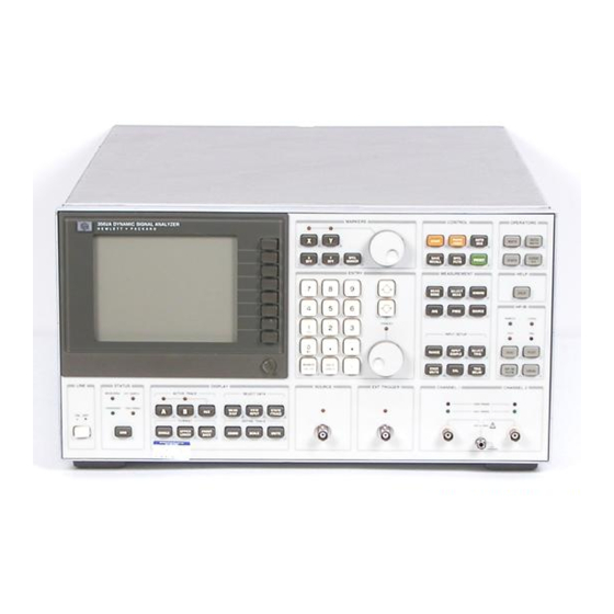
HOW THIS MAN UAL IS ORGANIZED adjust, and service the H P 3562A Dynam ic Signal Analyzer. Figure 1 -1 shows the front and rear views of the HP 3562A and figure 1 -2 shows the accessories su ppl ied with the H P 3562A. - Page 8 X·RAYS GENERATED IN THIS INSTRUMENT ARE E/BESCHL.SPG � 20KV SUFFICIENTLY SCREENED. DIE IN DIESEM GERAT ENTSTEHENDE ��������;;' � RONTGEN8TRAHLUNG 1ST AUSREICHEND REF IN -LINE ® EXT SAMPLE IN -VOLTAGE SELECTOR c::J SYNC OUT 1 -2 Figure Front and Rear Views ' 1 -1 HP 3562A...
- Page 9 *The number shown for the plug is the industry identifier for the plug only. The number shown for the cable is an HP part number. for a complete cable inc luding the p lug. **U L l isted for use in the U n ited States of America.
- Page 10 This section contains the O perational Verification and the TESTS Performance Tests. Use the operational verification for in- com ing and after-repair inspections. Use the performance tests to verify that the HP 3562A conforms to its pub- ished specifications. I I I ADJUSTMENTS This section describes the adjustment procedu res which will return the instrum ent to peak operating condition.
- Page 11 The fol lowi ng accessories are avai lable: Transit Case ....HP 921 1 -2663 The H P 3562A is a du al-channel, FFT-based network, spectrum and waveform analyzer...
- Page 12 To a vo id serious injury, disconnect the ac line power cord be fore removing or installing the ac line fuse. There are two voltage settings on the rear panel of the H P 3562A. Before con necting the Voltage settings l ine power cord or tu rning on the instru ment, verify the voltage selector switch is in the correct position for the input l ine voltage.
- Page 13 Cleaning Solvents only non-abrasive, non-corrosive cleansers. A sol ution of warm water and m i ld soap is recommended. The 3562A specifications are l isted in table 1 -3. These specifications describe the instru 1 -9 SPECIFICATIONS ment's warranted performance. Supplemental characteristics are intended to provide information usefu l in applying the i nstrument by giving typical, but non-warranted, per...
- Page 14 MOD E L G E N ERAL I N FO RMAT ION 3562 Specifications cont. Table 1 -3 and 2 are the recommended input connections. Case 3 Input Channel BNC Connector Input Signal Case 4 Input Signal A Input Channel BNC Connector Input Signal B Cases 3 and 4 are input connections which degrade...
- Page 15 ODE L 3562A G E N E RA L I N FO RMAT ION Specifications cont. Table 1 -3 Single channel, inputs connected as shown in Cases 3 and Accuracy Adder: 1-3. in fi gure Add ±0.35 dB ± 4.0° to the abso lute accuracy.
- Page 16 MOD E L G E N ERAL I N FO RMATION 3562 Specifications cont. T;�bJe 1 -3 1 -1 0...
- Page 17 Hewlett-Packard Graphics Language di gital plotters. The equ ipment req u i red to maintai n the H P 3562A is listed i n table Other equ ipment may be substituted for the recommended model if it meets or exceeds the listed critical...
- Page 19 D E L 3562A G E N E RA L I N FO RMATION Table 1 -4 Recommended Test Equipment cont. Recommended Instrument Critical Specifications Model Use* Probe, I m pedance: 10 M!) H P 1 001 4A A,F, Osci Iloscope...
-
Page 21: Table Of Contents
P E RFORMANCE TE STS L 3 562A SECTI O N P E RFO RMANCE TESTS Contents Page Paragraph Title Introduction ......... . . 2-1 /2-2 Cali bration Cyc le . - Page 22 MOD E L 3562 P E R FO RMAN C E T E STS Tables Number Title Page ..... 2-8· (OV) Amplitude Accuracy and Flatness 2-16 (OV) Common Mode Rejection ........2-23 (OV) Spurious Signals ........2-24 (OV) Noise Level ..........
-
Page 23: Introduction
Note: Tables and figures begi nning with "(OV)" are used in the operational verifica tion tests. To verify that the H P 3562A is meeti ng its publ ished specifications, the performance tests CALIBRATION CYCLE must be done every twe lve months. -
Page 25: Part A Operational Verification
Verification Test Record," paragraph 2-1 6. This test record may be reproduced without written permission of Hewlett-Packard. 5. If the HP 3562A fails a test, use the " I f Test Fai ls Check:" paragraph at the end of each test. - Page 31 O P E RAT IONAL V E R I F I CAT ION D. For each of the frequencies listed in table 2-1 perform steps 1 through 7: 1 . Press the HP 3562A keys as fol lows: To range setting in table C E N T E R FREQ .
- Page 33 SCALE k H z SCALE Perform steps 1 through 6: .375, 1 00 1 . Press the HP 3562A keys as fol lows: dBVrms SOU RC E LEVEL ..d BVrms RA N G E - 47...
- Page 34 MOD E L 3562 O P E RAT I ONA L V E R I FICATION 5. Press the H P 3562A keys as fol lows: d BVrms SOURCE LEVEL ..d BVrms RA N G E...
-
Page 35: Required Test Equipment
Section VI I A32, A34 Analog Digital Converter Boards A30 A nalog Sou rce Board This test measu res the freq uency accu racy of the H P 3562A . 2 - 1 1 FREQU ENCY ACCURACY Freq uency Synthesizer... -
Page 36: Initial Equipment Setup
Freq uency Synthesizer Frequency 99 kHz Ampl itude 1 Vrms Function Sine Wave C. Press the H P 3562A keys as fo l lows: RESET SI N G L E PRESET CA L d BVrms C E NTE R FREQ... - Page 37 OO E l 3562A O P E RAT IONA L V E R I FICATION This test measures the capab il ity of the 3562A to ignore a signal which appears 2-1 2 COMMON MODE REJECTION simu ltaneously and i n phase at the high and low input of a single channel.
- Page 38 B. Set the freq uency synthesizer as fol lows: Function Sine Wave H igh Voltage Output C. Press the H P 3562A keys a s fo llows: R ESET S I N G LE PRESET CA L E NT E R...
- Page 39 O P E RATI ONAL V E RI F I CATION · 2. Press the HP 3562A keys as fol lows: C E NT E R FREQ To signal frequency in table F REQ To range setting #1 i n table...
- Page 40 A33, A35 I nput Boards Section VI I A30 A nalog Sou rce This test measu res the phase accu racy of the H P 3562A relative to the phase of the trig 2-1 3 SINGLE CHANNEL PHASE ACCURACY ger signal. The freq uency synthesizer is used to input a squ are wave to one channel and the external trigger in put.
- Page 41 ODE L 3562A O P E RATIONAL V E R I FICAT ION HP 3562A DDD � oBB 8 FREQUENCY SYNTHESIZER DDD [gJ HP 3325A : : : I c=J � 18 8 8 8 8 1 O DD DD @ 000 8 ·...
-
Page 43: Noise And Spurious Signal Level
O D E L 3562A O P E RATI ONAL V E R I F I CATION G . Press the H P 3562A keys as fol lows: CHAN1 I N PUT SE LECT TRIG k H z START H . Record the Ya marker read ing o n the Operational Verification Test Record for CHAN 1 . - Page 44 VOLTS W I N DOW U N I TS U N ITS VO LTS C. Perform steps 1 through 4: 1 . Press the H P 3562A keys as fol lows: Y AUTO START SCA L E SCALE MRKR PEAK...
- Page 45 :;:; - 1 31 d BV D. For the rest of the start frequencies in tab le 2-3 perform steps 1 through 4: 1 . Press the HP 3562A keys as fol lows: To start freq uency in START FREQ...
- Page 46 1 . Press the H P 3562A keys as fol lows: START FREQ To start freq uency in table F REQ FREQ SPAN To freq uency span in table 2. When the average is complete, press the HP 3562A keys as fol lows: START MRKR PEAK SPCL MARKER 2-24...
- Page 48 STOP FREQ FREQ C. When the sweep is com plete perform steps 1 and 2 : START 1 . Press the H P 3562A keys a s fol lows: Y FIXD SCALE 9,1 1 d B SCALE 2 . If the trace i s between the 9 dB and the 1 1 dB lim its, check PASS o n the Operation Verification Test Record for the 0 to 65 kHz span.
-
Page 49: Self Test
. OD E L 3562A O P E RATIONAL V E R I FICAT ION 2- 1 6 OPERATIONAL VERIFICATION TEST RECORD 2-7 Self Test PASS 2-8 DC Offset Measured Value Specification Range Setti n'g C H AN 1 CHAN 2 - 51 dBV <... - Page 50 MOD E L 3562 OPE RATIONAL V E R I FICATION 2-1 2 Common Mode Rejection First Second Measurement Relative Value Measurement - Measu red Signal Fi rst Second Specification Value Frequency Meas urement Measu rement CHA N 1 CHAN 1 CHAN 1 �...
-
Page 51: Part B Performance Tests
2-42. This test record may be reproduced without written perm ission of Hewlett-Packard. 5. If the H P 3562A fails a test, use the " I f Test Fai ls Check:" paragraph at the end of each test. Y � - 3 5 l . 4 B 6 D Y �... -
Page 52: Required Test Equipment
I n each test, any u nspec ified parameters shou ld be set to the fol lowing con ditions: S I N E WAVE ( - ) Function HP 3325A F requency Synth esizer Freq uency 1 k H z Ampl itude... -
Page 53: Self Test
Sample Rate MAX IMUM H igh Resol utio.n. . . Auto Cal This test determ ines if the H P 3562A is operating correctly. No tests shou ld be attem pted 2-2 1 SELF TEST until the instrument passes this test. -
Page 54: Dc Offset Test Setup
MOD E L 3562 P E R FORMANCE T ESTS feedthrough termi nations HP 1 1 048C Requ i red Test Equi pment Table 2-5 DC Offset Range Setting Specification 7 d BVrms < - 23 d BV - 35 d BVrms <... -
Page 56: Amplitude Accuracy And Flatness
P E RFO RMANCE T ESTS MOD E L 3562 This test measures the ampl itude accu racy and flatness of the H P 3562A using the ampl itude 2-2 3 AMPLITUDE ACCURACY and FLATNESS reference of the ac cal ibrator. -
Page 57: Amplitude Accuracy And Flatness Test Setup
M OD E L 3562A P E R FORMANCE T ESTS AC CALI BRATOR FLUKE 5 2 0 0 A PHASE LOCK INPUT REAR PANEL V I EW FREQUENCY SYNTHESIZER HP 3325A 00000 0 0 0 . 00000 00000 0 ·... - Page 58 P E R FORMANCE T E STS MOD E L 3562 C. Press the H P 3562A keys as fol lows: R E S E T S I NG LE PRESET CA l G ROUND CHAN 1 I N P U T...
- Page 59 P E R FORMANCE T E STS D. For each of the frequencies listed in tab le 2-6 perform steps 1 through 7. 1 . Press the H P 3562A keys as fol lows: To range setting i n table...
- Page 60 C . Reverse the banana plug con nector at the ac cal ibrator so the high input signal goes to the BNC shell of H P 3562A's input channels. The BNC center condu ctor shou ld be grou nded for each channel.
-
Page 61: Amplitude Linearity
P E R FORMANCE TE STS This test measures the amplitude linearity of the H P 3562A by using the ampl itude reference 2-24 AMPLITUDE LINEARITY of the ac calibrator. If the measu rement of a signal is between the BNC center conductor and BNC shell and... -
Page 62: Amplitude Linearity Test Setup
1 1 0 0 1 - 6 0 0 0 1 � BANANA/BANANA Figure 2-1 3 Amplitude Linearity Test Setup C. Press the HP 3562A keys as fol lows: R E S ET S I N G L E PRESET... - Page 63 1 .000 mVrms 2.51 7 mVrms - 51 7.1 uVrms 2.559 mVrms - 555.9 uVrms 1 . Set the ac calibrator's ampl itude. 2 . Press the H P 3562A keys a s fol lows: START MRKR PEAK SPCL MARKER 3.
- Page 66 D I SP k H z SCA LE SCALE C. Perform steps 1 through 6: .375, 1 00 1 . Press the H P 3562A keys as fol lows: d BVrms dBVrms SOURC E LEVEL ..- 47 RANGE...
- Page 68 MO D E L 3562 P E RFO RMAN C E T E STS 5. Press the H P 3562A keys as fo l lows: dBVrms d BVrms SOURC E LEVEL ..RA N G E SO U RCE...
- Page 71 1 Vrms Ampl itude 1 56 kHz Frequency Fu nction Sine Wave C. Press the H P 3562A keys as fol lows: R E S E T S I N G LE PRESET Vrms E NT E R RA N G E...
-
Page 73: Frequency Accuracy Test Setup
99 kHz 1 Vrms Ampl itude Sine Wave Fu nction C. Press the H P 3562A keys as fo l lows: R E S E T S I NG L E PRESET d BVrms C E N T E R FREQ... -
Page 74: Input Coupling Insertion Loss Test Setup
H P 3325A Freq uency Synthesizer Req u i red Test Equi pment feedthrough termination H P 1 1 048C BNC Tee H P 1 250-0781 mrnooo[gJ HP 3562A FREQUENCY SYNTHESIZER HP 3325A ggggg 0 · 00000 8NC CA8LE 8120-1838... - Page 75 Freq uency Synthesizer 1 H z Frequency 1 Vrms Ampl itude Sine Wave Function C. Press the H P 3562A keys as fol lows: R E S ET S I NG LE PRESET Vrms FREQ S PAN RA N G E...
-
Page 77: Single Channel Phase Accuracy Test Setup
10 kHz to 1 00 kHz ± 1 6.0 degrees Frequency Synthesizer H P 3325A Req u i red Test Equi pment 500 feedthrough term ination HP 1 1 048C (2) BNC Tees H P 1 250-0781 §o� HP 3562A O DD... - Page 78 MOD E L 3562 PERFORMANCE TEST C. Press the H P 3562A keys as fol lows: R E S E T S I N G LE PRESET POWE R S PEC SHECT MEAS G ROUND C HAN1 I N P U T...
- Page 79 D. For each of the frequencies listed in table 2-1 1 perform steps 1 through 4: 1 . Set the freq uency Synthesizer as follows: To signal freq uency in table Frequency 2. Press the HP 3562A keys as fol lows: To trigger slope in table SE LECT To trigger type in table...
-
Page 81: Input Resistance Test Setup
Function 2 W I RE OHM Range AUTO I NT E RNAL Trigger Press the HP 3562A keys as fol lows: R E S E T S I N G LE PRESET G RO U N D CHAN 1 I N P U T... -
Page 82: Input Capacitance Test Setup
D. For each of the range settings I isted in table 2-1 2 perform steps 1 and 2: - 1 3 d BVrms 1 050 1 . Press the H P 3562A keys as fol lows: T o the range setting i n table RANG E 2. -
Page 85: Harmonic Distortion
OD E l 3562A P E R FORMANCE TESTS This test measures the harmonic d istortion generated in the H P 3562A when a full scale 2-3 1 HARMONIC D ISTORTION input is present. The relative ampl itude of all harmonics w i l l be at least 80 dB below the fu ndamental Specification ampl itude. - Page 87 P E R FORMANCE TE STS O D E L 3562A 2. Press the H P 3562A keys as fo llows: C E NTE R FREQ To signal frequency in table F REQ Ave OFF START To signal freq uency in tab le S I N G LE 3.
-
Page 88: Harmonic Distortion Test Setup #2
E. For measurement two, connect the test instru ments as shown in figure 2-22. The chassis grou nd cable must go to the grou nd term inal of the low distortion osci llator. F. Press the HP 3562A keys as fol lows: FLOAT C HAN 1... -
Page 89: Intermodulation Distortion Test Setup
H P 3562A to the 4th order. NOTE The HP 3325A may produce some spurious signals in the 0 to 1 00 kHz span. Ignore signals at frequencies other than those listed in the tables when performing th is test. - Page 90 26 kHz Ampl itude 1 Vrms Function Sine Wave C. Perform steps 1 through 5: 1 . Press· the H P 3562A keys as fol lows: R E S ET S I NG LE PRESET Vrms RA N G E...
- Page 93 OD E L 3562A F. For each of the harmonic frequencies l isted in table 2-1 4 perform steps 1 through 1 . Press the H P 3562A keys as fol lows: C E N T E R FREQ To harmonic frequency...
- Page 94 MO D E L 3562 4. Adjust the ampl itude of frequency synthesizer #2 u ntil Ya dB ± 50 mdB. 5 . Press the H P 3562A keys as fol lows: STA BLE Table 2-1 5 Intermodulation Distortion Measurement Two...
-
Page 95: Noise And Spurious Signal Level
BBoG ° 000 000 0 0 0 HP 1 1 0 4 8 50 OHM FEEDTHROUGH TERM I NA T I ONS A L L I G A T O R C L I P CABLES Figure 2-2 5 Noise and Spurious Signal Level Test Setup... - Page 96 P S PEC VOLTS W I N DOW UN ITS U N ITS VOLTS C. Perform steps 1 through 4: 1 . Press the H P 3562A keys as fol lows: Y A UTO START SCALE SCALE MRKR ..PEAK...
- Page 97 ::5 - 1 31 d BV D. For the rest of the start frequencies in table 2-1 6 perform steps 1 through 4: 1 . Press the H P 3562A keys as fol lows: STA RT FREQ To start frequency i n...
- Page 98 UN ITS U N ITS F. For each of the start frequencies listed in tab le 2-1 7 perform steps 1 through 5: 1 . Press the H P 3562A keys as fol lows: START FREQ To start frequency in...
-
Page 101: Cross Talk Channel 2 Test Setup
SCALE - 1 40,23 D . Using the marker knob, move the Y marker to the center of the X marker dot and press the H P 3562A keys as fol lows: H O LD Y U P PER E . Using the marker knob, move the Y marker to the center of the X marker dot. -
Page 102: Common Mode Rejection
Trou bleshooting A33, A35 I nput Boards Section V I I I This test measures the capabil ity of the 3562A to ignore a signal which appears 2-3 5 COMMON MODE REJECTION simu ltaneously and in phase at the high and low in put of a single channel. -
Page 103: Common Mode Rejection Test Setup
F BARREL BNC/BNC 1 25 0 -OOBO B 1 20 - 1 B40 C. Press the H P 3562A keys as follows: Figure 2-28 Common Mode Rejection Test Setup # 1 R E S E T S I NG LE PRESET... -
Page 105: External Reference Test
EXTERNAL REFERENCE TEST is within the specified range. The H P 3562A w i l l lock to external signals ()f 1 , 2, 5, and 1 0 MHz ± 0.01 % . The ampl itude Specification of the signal m ust be between 0 d Bm and + 20 dBm . - Page 106 MOD E L 3562 PERFO RMAN C E TE STS A. Connect the H P 3562A as shown in figure 2-30. Refer to " I n itial E q u ipment P rocedu re Setup," paragraph 2-20, for unspecified parameters.
-
Page 107: Source Residual Offset
B. Set the d igital voltmeter as fol l ows: Function dc (==V) Trigger I nternal Range Auto C. Press the H P 3562A keys as fo llows: R E S E T S I NG LE PRESET SOURCE LEVEL FIXE D S I N E SOU RCE... -
Page 110: Source Output Resistance Test Setup
H P 1 0502A Figure 2-32 Source Output Resistance Test Setup Con nect the test instruments as shown in figure 2-32. Proced u re Press the HP 3562A keys as fo l lows: R E S E T S I NG LE PRESET... -
Page 113: Source Energy Measurement
A30 Analog Sou rce Board Section VI I A4 Local Oscillator Board This test measures the in-band energy of the H P 3562A noise source using the power marker 2-41 SOURCE ENERGY MEASUREMENT fu nction of the H P 3562A and a true rms voltmeter. - Page 114 B. Set the test instruments initially as fol lows: Digital Voltmeter Function ac V ( - V) Trigger I nternal C. Press the HP 3562A keys as fol lows: R E S E T S I NG LE PRESET G ROUND C HAN 1...
- Page 115 STO RE RECALL 3. Record the voltmeter average on the Performance Test Record. Record the H P 3562A power measurement o n the Performance Test Record. Press the HP 3562A keys as fol lows: PR IODC C H I R P...
-
Page 117: (Ov) Amplitude Accuracy And Flatness
OD E L 3562A P E R FORMANC E TESTS 2-23 Amplitude Accuracy and Flatness Measurement One BNC shell grounded Measured Value Specifi cation Range Signal Setting Freq uency Lower Limit U pper Limit C H AN 1 CHAN 2... -
Page 118: Amplitude Accuracy And Flatness Measurement Three
PE RFO RMAN C E TE STS MOD E L 3562 2-23 Amplitude Accuracy and Flatness Measurement Three BNC center conductor grou nded Measured Value Specification Range S ignal Setting Frequ ency Lower Limit Upper Limit C H AN 1 C H AN 2 8 d BV 1 k H z... -
Page 119: Anti-Alias Fi Lter Response
P E R FO RMANCE TE STS OD E l 3562A 2-25 Amplitude and Phase Match BNC s hel l grounded PASS PASS Range Part Amplitude Part Phase Setti ng Specification Specification - 49 d BV ± 0.1 d B ±... -
Page 120: Single Channel Phase Accuracy
P E R FORMANCE TE STS MOD E L 3562 2-29 Single Channel Phase Accu racy BNC shell grounded Signal Measured Value Frequency Trigger Specification Slope Type Lower Limit U pper Limit C HAN 1 CHAN 2 pa s CHAN 1 - 92.5 °... -
Page 121: Resistance Measurement
PERFO RMANCE TESTS O O E L 3562A 2-30 Input Impedance Resistance Measurement Measured Value Range Setting Specification Lower Limit Upper Limit CHAN 1 CHA N 2 20 d BV 1 050 1 050 - 1 3 d BV 1 050... -
Page 122: Intermodulation Distortion Measurement One
PE RFORMANCE TESTS MOD E L 2-32 Intermodulation Distortion Measurement One BNC shell grounded C h annel 1 Channel 2 PASS PASS H armon ic Frequency Specifi cation Specifi cation 6 k H z :::s; - 80 d B :::s; - 80 d B :::s;... -
Page 123: Spurious Signals
OD E L 3562A P E R FORMANCE TE STS 2-33 Noise and Spurious Signal Level Spu rious Signals PASS PASS Start Frequency S pecifi cation Frequency Span CHAN 1 CHAN 2 20 H z 1 k H z :5 - 1 31 d BV... -
Page 124: Common Mode Rejection
MOD E L 3562 PE RFORMANC E T E STS Common Mode Rejection 2-35 First Second Relative Value Measu rement Measu rement Measured Signal First Second Specification Value Frequ ency Measurement Measu rement CHAN 1 CHAN 1 C H AN 1 66 H z �... -
Page 125: Source Distortion
2: 40 d B 5 Vpk 99 kHz 2: 40 d B 2-41 Source Energy Measurement Random Noise: HP 3562A Read ing (- - r - ) X 1 00 2: 70% Voltmeter Average ( % in-band energy Period ic Ch irp:... - Page 127 ODE L ADJ USTM E NTS 3562A S ECTI O N I I I ADJ USTM E NTS Contents Paragraph Title Page Introdu ction ..........
- Page 129 ADJ USTM E NT S SE CTI O N I I I ADJ USTM E NTS This section describes adj ustments and checks required to bring the H P 3562A within the INTRODUCTION specifications l isted in Table If adjustments are made to a particu lar board, all adjust...
- Page 131 2 . Remove the H P 3562A bottom cover. None of the internal covers need to be removed . 3 . If the mains power voltage selector (on the rear panel) i s not in the 1 1 5V setti ng, switch it to 1 1 5V.
- Page 132 MODE L 3562 ADJ USTM E NTS NOTE: The A1 8 board runs the le ngth of the in stru ment underneath the Board display, and is accessed Location from below by removal of the bottom cover. TP1 2 Figure 3-1 Power supply component locator (A 1 S) Description: 20.48 MHz REFERENCE ADJ USTMENT...
- Page 134 MOD E L 3562 ADJ U STME NTS Board A I . Location TP1 0 Trigger board component locator (A3 1 1 Figure 3-2...
- Page 135 O D E L 3562A ADJ USTM E NTS Special note: capacitive load may be used to reduce noise on the scope display in the fol lowing adjustment. This part is not req u i red to perform this adjustment, but it does make it easier to evaluate the resu lts the first few times through the procedu re.
- Page 136 ADJ U STME NTS MO D E L 3562 NOTE Pressing the beeper key toggles the beeper between on and off. It does not matter whether the beeper is turned on or off as long as the keys are pressed in the order spec ified. If beeper comma nds have been activated, the instrument must be reset before it can make measurements.
- Page 137 This completes the adjustment. If no more adjustments are to be made to this board, remove the l ine power cord from the H P 3562A rear panel, remove the extender board and reinstall the ADC board in the card cage.
- Page 138 Disconnect the l i ne power cord from the rear panel of the H P Remove the ADC board to be adjusted and place it on the extender board. 3562A. Recon nect the l ine power cord and turn the power switch ON.
- Page 139 O D E L 3562A ADJ USTM E NTS Board Location ) 200 U200 RN200 TP400 R400 R401 TP40S Figure 3-9 ADC board component locator (A32) & Figure 3-1 0 Both R401 R400 Figure 3-1 1 R401 adjusted to out of adjustment flatten "no isy "...
- Page 141 This com pletes the adj ustment of the ADC board. Remove the li ne powe r cord from the H P 3562A rear panel, retu rn ju mper 1 300 to the upper two pins (normal position), remove the shorting clip between TP400 and ground, remove the extender board and re insta l l the ADC board in the card cage.
- Page 142 To adjust channel two, also press: . . . POW E R SPEC2 7. Adjust A33R21 2 for a marker ampl itude read i ng of less than - 85 dB on the H P 3562A MEAS D I S P ·...
- Page 147 ADJ USTME NTS 3562A I OD E L Board Location � Figure 3-1 6 Analog source component locator; A30R9 3-1 9...
- Page 149 A D J USTME NTS Board Location Figure 3-1 7 Analog source component locator; A30R 1 0 3-21 /3-22...
- Page 153 A". m bl ' �\ �". " ' N"mb" A1 2 R22 2. HP PART N UM B E R 3 . C D - The Check Digit used by H P to verify that an order has been transm itted correctly.
- Page 155 R E PLACEABLE PARTS Figure 4-2 Cabinet Parts, Exploded View C urrent Previous Part N umber Part N umber MP#* Description Q ty (Metric)** (English)** Front frame 5021 -5807 5020-8807 Rear frame 5021 -5808 5020-8808 Front handle kit (optional) 5061-9691 5061-0091 Trim, front handle 5020-8898...
- Page 156 MOD E L REPLAC EABLE PARTS Reference Designations and Abbreviations Table 4-1 Abbreviations negative positive zero . si lver NPO . Ag . (zero temperature c efficient) . aluminum A I . nanosecond(s) 10 - seconds ampere(s) ..not separately replaceable .
- Page 157 R E PLACEABLE PARTS Figure 4-2 Cabinet Parts, Exploded View Previous Current Part Nu mber Part Number (Metric)* * (English)** Description Q ty MP#* 5020-8807 5021-5807 Front frame 5020-8808 5021 -5808 Rear frame 5061-9691 5061-0091 Front handle kit (optional) 5020-8898 Trim, front handle 5040-7202 Top trim, front frame...
- Page 158 MOD E L 3562 R E P LACEABLE PARTS Table 4-1 Reference Designations and Abbreviations Abbreviations ..negative positive zero ..silver NPO . Ag . . (zero temperature coefficient) . a luminum ·...
- Page 159 R E PLACEABLE PARTS Table 4-2 Manufacturers Code List Z IP CODE A D D R E S S MAN U FACTURER NAME N O . H9027 17105 00779 29671 00853 Luzern Sehurter A G H 53204 01121 Harrisburg Amp Ine 75222 01295 Pickens...
- Page 161 R E PLACEABLE PARTS ODE L 3562A Table 4-3 Replaceable Parts Reference HP Part Mfr Part Number Description Code Designation Number 2 8 4 8 0 0 3 5 6 2 - 6 6 5 0 1 0 3 5 6 2 - 6 6 5 0 1...
- Page 162 MOD E L 3562, R E P LACEABLE PARTS Table 4-3 Replaceable Parts cont. Reference HP Part Mfr Part Number Description Qt y Code Designation Nu mber IC DRVR TTL NOR QUAD 2-INP 0 1 2 9 5 S N 4 3 2 6 6...
- Page 163 R E P LACEABLE PARTS Table 4-3 Replaceable Parts cont. Reference HP Part Mfr Part Number Q t y Description Code Designation Nu mber 1 9 7 0 1 5 0 3 3 R R l - R 2 0757-0280 RESI STOR l K 1% .
- Page 164 MOD E L R E P LAC EABLE PARTS Table 4-3 Replaceable Parts cont. Reference H P Part Mfr Part Number Q t y Description Code Designation Number 0 1 29 5 SN1 1 1 0 8 N IC DRVR TTL LS LINE DRVR OCTL A2U5 1 2 1 8 20-21 1 0 0 1 2 6 3...
- Page 165 R E PLACEABLE PARTS Table 4-3 Replaceable Parts cont. Reference HP Part Mfr Part Number Description Qt y Code Designation Number 28480 0 3 5 6 2 - 6 0 3 6 3 3U20 1 0 3 5 6 2 - 6 0 3 6 3...
- Page 166 MOD E L 35621 RE PLACEABLE PARTS Table 4-3 Replaceable Parts cont. Reference HP Part Mfr Part Nu mber Description Q t y Code Designation Number RESISTOR . 1 25W F TC=0+- 1 00 1 9 7 0 1 5 0 3 3 R...
- Page 167 R E PLACEABLE PARTS Table 4-3 Replaceable Parts cont. Reference HP Part Mfr Part Number Description Code Designation Nu mber IC FF TTL ALS D-TYPE POS-EDGE-TRIG 0 1 2 9 5 SN7 1 1 7 1 N U 7 3...
- Page 168 MOD E L 35621 V\ R E P LACEAB LE PARTS Table 4-3 Replaceable Parts cont. Reference HP Part Mfr Part Number Description Q t y Code Designation Number NETWORK-RES 1 0- S I P 4 . 7K OHM X 9...
- Page 169 R E PLAC E A B LE PARTS Replaceable Parts cont. Table 4-3 H P Part Mfr Part Number Description Qt y Code Number 0 1 29 5 SN7 1 1 7 3 N 1 8 20-2657 I C GATE T T L A L S O R QUAD 2 - I NP 1 0 4 0 1 29 5 SN7 1 3 3 8 N...
- Page 170 MOD E L 356',A R E P LACEABLE PARTS Replaceable Parts cont. Table 4-3 Reference HP Part Mfr Part Number Q t y Description Code Designation Number R - 2 5 J RESISTOR 4 . 7K 5% . 2 5W CF TC=0-400...
- Page 171 R E PLAC EABLE PARTS Table 4-3 Replaceable Parts cont. Reference HP Part Mfr Part Number Description Code Designation Number HM4 86 4 P - 3 1 8 1 8 - 30 0 6 IC NMOS 6 5 5 3 6 ( 6 4 K ) D Y N RAM...
- Page 172 MO D E L 3562 f'\ R E P LAC EABLE PARTS Table 4-3 Replaceable Parts cont. Reference HP Part Mfr Part Number Qt y Description Code Designation Nu mber 1 9 9 0 - 0 6 5 2 LED-LAMP ARRAY LUM- I NT = 2 0 0 U C D IF=5MA-MAX...
- Page 173 R E P LACEABLE PARTS ODE L 3562A Replaceable Parts cont. Table 4-3 Reference HP Part Mfr Part Number Description Code Designation Number 2 8 4 8 0 1 2 5 2 - 1 1 8 7 1 25 2- 1 1 8 7 CONN-POST-TP-HDR 40 P I N .
- Page 175 R E PLAC EABLE PARTS Table 4-3 Replaceable Parts cont. Reference HP Part Mfr Part Nu mber Q t y Description Code Designation Number CAC02COG39 1 J l 00A 0 1 6 0- 48 0 9 CAPACITOR-FXD 390PF +-5% 1 00VDC C E R...
- Page 177 R E P LAC EABLE PARTS Table 4-3 Replaceable Parts cont. Reference HP Part Q t y Description Mfr Part Number Designation Number Code 1 8R 4 8 0 6 9 8 - 32 0 2 RESISTOR 1 . 7 4 K 1 % . 1 25W F TC=0+ - 1 00...
- Page 178 MOD E L 35621'\ R E P LACEABLE PARTS Table 4-3 Replaceable Parts cont. Reference HP Part Mfr Part Number Q ty Description Designation Code Number A 1 8 R 5 0 3 0 6 9 8 - 4 4 0 8 R E S I STOR 1 24 1 % .
- Page 179 R E PLACEABLE PARTS Table 4-3 Replaceable Parts cont. Reference HP Part Mfr Part Number Q t y Description Designation Number Code 2 3 60-0 1 2 1 SCREW-MACH 6 - 3 2 . 5 -IN-LG PAN-HD-POZI 0 1 5 36...
- Page 180 MOD E L R E P LACEABLE PARTS Table 4-3 Replaceable Parts cont. Reference HP Part Mfr Part Number Description Q t y Code Designation Number 7 1 707 2900-0022 RELAY-REED lA 500MA 200VDC 5VDC-COIL A30K200-K202 0 4 9 0- 1 403...
- Page 182 MODE L 3562 R E P LAC E A B LE PARTS Replaceable Parts cont. Table Reference HP Part Mfr Part Number Description Code Designation Number CAPACITOR-FXD . 0 1 UF + - 1 0% 1 00VDC CER 27 1 6 7...
- Page 183 R E P LACEABLE PARTS Replaceable Parts cont. Table Reference HP Part Mfr Part Number Q t y Description Code Designation Number 0 6 9 8 - 6 3 4 8 RESISTOR 3K . 1 % . 1 25W F T C = 0+-25...
- Page 184 MOD E L 3562 R E PLACEABLE PARTS Table 4-3 Replaceable Parts cont. Reference HP Part Mfr Part Number Description Code Designation Nu mber RESISTOR . 1 25W F TC=0+ - 1 00 1 9 7 0 1 5 0 3 3 R...
- Page 186 MOD E L 3562A R E P LACEABLE PARTS Table Replaceable Parts cont. Reference HP Part Mfr Part Number Description Q ty Code Designation Nu mber 9 1 6 37 CMF-55- 1 , T - l RESI STOR 10 1 % .
- Page 187 RE PLAC EABLE PARTS Table 4-3 Replaceable Parts cont. Reference HP Part Mfr Part Number Description Code Designation Number RESISTOR 1 . 8 7K 1% . 1 25W F TC=0+ - 1 0 0 9 1 6 37 CMF-55 - 1 , T - 1...
- Page 190 R E P LACEABLE PART[:> MOD E L 3562A Replaceable Parts cont. Table Reference HP Part Mfr Part Number Description Code Designation N u mber 1 36 0 6 1 5 0D335XO O 1 5A2-DYS CAPACITOR-FXD 3 . 3UF+-20% 1 5VDC TA...
- Page 191 MOD E L 3562A Replaceable Parts cont. Table HP Part Mfr Part Number Q t y Description Code Number A3 Q l 05 1 8 5 3-0037 TRANSISTOR PNP SI TO-39 PD= l W FT= 1 00MHZ 047 1 3...
- Page 193 MOD E L 3562A R E LAC E A B L E PARTS Replaceable Parts cont. Table HP Part Mfr Part Nu mber Description Code esignation Number M P 2 2 9 1 35-026 1 L I N E FILTER...
- Page 194 RE PLACEABLE MO D E L 3562A Replaceable Parts cont. Table Reference HP Part Mfr Part Number Description Code Number Designation 2 8 4 8 0 5 0 4 1 - 2 9 9 0 5 0 4 1 - 2 9 9 0...
- Page 197 ....5-1 7 A22 HP- l B ....
-
Page 199: Introduction
The i nformation in this section documents the earl ier instrument configurations and assoc iated servicing procedu res. As Hewlett-Packard continues to improve the performance of the H P 3562A, corrections MANUAL CHANGES SUPPLE MENT and modifi cations to the manual may be req uired. Required changes are documented by a yellow Manual Changes supplement and/or revised pages. - Page 201 MANUAL BACKDATING OD E L 3562A 4. Change the A4 schematic in section IX as shown in figure 5-A4a. (7 ) U I 8 (8) FL l P - FLOP U40(9,12) U I 2 ( i 0 ) U45(3) 10 MODE...
-
Page 202: A5 Digital Filter
MOD E L 356J MAN UAL BACK DAT I NG 5. Change the com ponent locator as shown in figure 5-A4b. Figure 5-A4b Local Oscillator Component Locator Revision A Cu rrent revision: E 5-8 A5 DIGITAL FILTER Previous revisions: A l l revisions are electrical ly the same as revision E . Revisions A through D: The fol lowing components are i n sockets: Component Socket Part N umber... -
Page 203: A6 Digital Filter Controller
ODH 3562A MAN UAL BACKDAT I NG 2. Change test point labels as fol lows: Test Point Rev A Other Revs. C H FB1 CH1 FB1 TP1 0 C H FB2 CH1 FB2 TP1 4 CH1 S RT CH1 STRT... -
Page 205: A 1 7 Display Interface
OD E L 3562A MANUAL BACK DAT I NG Current revision: A 5-1 5 A 1 7 DISPLAY INTERFACE Previous revisions: None Current revision: C 5-1 6 A 1 8 POWER SUPPLY Previous revisions: Revisions A and B d iffer from revision C as fol lows: 1 . - Page 207 MOD E L 3562A . CR' �...
- Page 208 MAN UAL BACKDAT I NG <> R4&& R 4 1 3 R"a2 � l � � c"a" c"a3 " CWLJ Figure t Ba Power Supply Component Locator Revision 5-9/5-1 0...
- Page 209 MOD E L 3562A...
- Page 210 MAN UAL BACK DAT I N G Ri92 Ci93 ; Figure Power Supply Component Locator Revision 5-A t ab 5-1 1 /5-1 2...
- Page 213 - - - - - - - - - - - - - - - - - - - - - - - - - - - - - - - - Su P PL Y- - 03562-66518 REV 8 P·AN EL.ii .
- Page 214 - . - - , - · C 4 0 1 + 8 S 1 � + 1 5 I S I t! . � : ' J 4 0 0 ..1...
-
Page 215: A22 Hp- L
MOD E L 3562A MANUAL BAC KDAT I N G C u rrent revision: A 5-1 7 A22 HP-IS Previous revisions: None C u rrent revision: 5 - 1 8 A30 ANALOG SOURCE Previous revisions: Revision B is electrically identical to revision C. - Page 218 � ... 1 (JS2-19, 20) (JS4-19, 20) ASO (JSO-40) AS2 (JS2-2S, 24) AS4 (JS4-2S, 24) Ai (J1-U9, 120) A4 (J4-U9, 120) A5 (J5-U4) AB (JB-US) A1B (N1S) 5-1 7/5-1 8 Figure Trigger Schematic Revision 5-A3 1 b...
- Page 219 MOD E L 3562A MAN UA L BAC KDAT I NG 1 . The fol lowing components are not on revision A: Reference HP PIN R209 0757-0442 81 50-3375 2. The following test locations on revision A correspond to the test points listed...
- Page 222 - - - - - - - - - *A34 J200 L605 L601 250pF +5VR C609 C610 + L604 22pF +15V 100 pF C402 A 1 B (WI3) C4 03 O . 1 � � O . 1 � O . 1 22P F �...
- Page 223 03562-66533 INPUT 2 03562-66535 *WHERE NOTED J300 HIGH INPUT (SNC CENTEA) fROH fRONT PANEL W1 (HP104) A 30 (9) COPYFiISHTtI;'5 1985, HEWLE1;- PACKARO To '-...
- Page 224 A3� CQVLCLI...
-
Page 225: Title Page
A2 Svstem CPU/HP I S ........ - Page 226 HP 3562A Block Diagram ........
- Page 227 C I RC U IT D ESCRI PTIONS MOD E L 3562A HP- I B KEY BOARD d i gital I NPUT analog s ignal signal control line D I G ITAL D I S PLAY FRONT COMMON BUS control l ines I NT ERFACE + 2 .6V...
- Page 228 The overall instru ment description describes the interaction of the H P 3562A's individual assem bl ies. Use this section to gain an overa l l u n derstanding of the H P 3562A's operation. Use the circuit descriptions along with the schematics in Section IX to u nderstand the operation of an assembly.
- Page 229 C P U H P-I B K E Y B O A R D I N PUT C H A �� �� fL 1 analog digital � C H A N N E L 1 signal C H AN N E L control line I N P U T...
- Page 231 InO 3J�nOS :l 3 � � 3 �� 1 �1 1X3 31dWVS lX3 l 1 3 N N V H )
- Page 232 SYST E M C P U (68000) H P- I B K EY B OA R D E L 1 ..S i gnal S ignal control D I G I TA L l i ne F I LT E R D i g ital Analog A D C...
- Page 233 CI-I.A NN E l 1 anall signi cantl line I N P U T CHA N N E L 2 C I-I A N N E l 2 EXT SAMPLE I N T R I ( EXT T R I G G E R R E F I N S O U RC E O U T ANALOG...
-
Page 234: Block Diagram
F . E . I N T E RFACE I N T E R FA C E digital signal H P 1 3 45A �+2 ' 6 V � 'i V ±8V A1 7 ±15 V ± .W V A1 8 Figure Block Diagram 3562A 6-9/6-1 0... - Page 235 (US-6) (U S-S) (U3-17) CLRL (U3-1 2) ALUCK (U 3-1 S) (U 3-1 3) (U3-1 4) DACEN (U3-16) F5L D (U3-1 S) DACDAT (U209-6) CO UNTER ¥...
- Page 236 510 51 1 51 3 51 4 51 5 51 6 51 7 51 8 51 9 520 521 Figure a Digital Source Timing 6-A 1 6-1 3/6-1 4...
- Page 237 Sample C l ock (SAMP) NOTE: F U L L S PA BASi BAI MODE...
- Page 238 D S E L CONTROL R E G I ST E RS B U R S T 2.56 M H z CONTROL C I RC U I T 2.56 M H z Sample PROG RAMMABLE 256 KHz MULTI- l i N E C O U N T E R S P L l E R M U L T I-...
- Page 239 MO D E L 3562A C I RCUIT D E SCR I PT I O N S (Refer to figure 6-A 1 c) The phase resolution circuit is used in external and internal trig Phase Resolution Circuit gered measurements. This circu it insures that the phase of a triggered measurement is accu rate.
- Page 241 C I RC U I T D E SC R I PT I O N S MODE L 3562A (Refer to figure 6-A1 d) The burst control circuit controls the burst length and generates Burst Control Circuit the pu lse signal (NC LK) to the local osc i l l ator. It provides the gating signal (BU RSTE N) that gates the analog source on and off during the burst and chirp modes.
- Page 242 C I RC U IT D ESCRI PTIONS MOD E L 3562A (Refer to figure 6-A1 e) The pu rpose of the LO input receiver is to synchron ize the local LO Input Receiver oscil lator input data (NDA T) to the sam ple rate (SAMP). This is necessary because in external sample mode the LO data does not come at a regular rate.
- Page 247 System Add ress A D D R E S S A1 L To A8L COMPARATOR STESl System Data DATA B U S DO TO D1 5 DS Data Bus B U F F E RS Write To Control RESL E N A B L E L R E S ET L D E V I C E D E V I C E...
- Page 248 To A l l Functional Blocks in Test Mode S E LCNTRSL SYNC TEST B U RST T I M I N G S E LCNTRSL BURSTEN R E G I ST E R CONTROL CONTROL NCLK I n put Noise Receiver Generator...
- Page 249 MOD E L 3562A C I RC U I T D E SC R I PT I O N S Refer to Figure 6-A2 for this discussion. The processing unit of the A2 System C PU (Central A2 SYSTEM CPU/HP'S Processing U n it) is a MC68000 1 6-bit m icro processor.
- Page 250 MOD E L 3562A C I RC U I T D ESCR I PTIONS 4. The system processor asserts upper d ata strobe (UDSL) and/or l ower data strobe (LDSL) signals to transfer byte data (8 bits) or word data (1 6 bits). The assembly being addressed determi nes whether UDSL or LDSL are used.
- Page 251 MO D E L 3 562A C I RC U I T D E SC R I PT I ON S Programmable Timer Module The programmable timer mod u l e is an i nternal time base generator, cl ocked by the E N B L clock fro m the system processor.
- Page 252 CPU DATA BUS Dc/> STATUS LEDs STAT U S STATUS D E COD E R A N D PWR UP POW E R U P/DOWN A D D R E S S UDSL D E C O D E R LDSL R/WL SYST E M...
- Page 253 CONTROL L I N ES CONTROL L I N E S TO SYSTEM BUS SYST EM BUS C O N T R O L D R I V E R SYSTEM ADDRESS BUS SYSTEM A1 Lto A23L A D D R E S S D R I V E R CPU DATA BUS MO N ITOR...
- Page 256 The A3 ROM board functions as an extension of read only memory for the system CPU board . The ROM board stores most programs for the HP 3562A exce pt i n itial start-u p routi nes. A l l com m u n i cations between the system C P U board and the ROM board occu r over the system bus.
- Page 258 C I RC U I T D E SC R I PT I O N S MOD E L 3 562A 8 MHz WRITEL A1 -A23 Valid Address ROMSE LL CE1 L-CE20L DTACKL FIgure 6-A3a TImIng DIagram 6-35/6- 36...
- Page 259 A22L '" � >- 8 MHz A23 L I nverting A1 L-A21 L D rivers...
- Page 260 ROM S E LL DTACKL Address Delay Comparator Data System Memory CE1 L-CE20L Data DOL-D1 5 L Decoders Driver Data A1-A1 6, O E L / A1 7 ROM Block Figure 6-A3b Diagram 6-37/6-38...
- Page 261 MO D E L 3562A C I RC U I T D E SC R I PT I O N S A4 LOCAL OSCILLATOR Introduction (Refer to figure 6-A4) The A4 Local Osc i l l ator (LO) prod uces d igital sine and cosine s ignals which are synchron ized with the sample rate.
- Page 262 C I RC U I T D E SC R I PT I O N S MO D E L 3S62A The AS D igital Fi lter sends the SYNC2 s ignal to the LO when it is ready for the next s i ne a n d cosine wave data po i nts.
- Page 264 SYSTEM Phase Data From ADDRESS M00 to M07 System CPU From System CPU SYSTEM INTERFACE From DATA ( System CPU From A1 BFST Digital Source LD€ VALOUT...
- Page 265 From AS Digital Filter SYNCZ Commands From A31 A1 Source Timing & Mode N SYNC To Dig ital Sou rce CONTROL & TIMING PHASE C I RCUITS ,CCUMULA TOR--" ..c Timing & Select Out Sine & I nterpolator ROMs Addresses PHASE S I N E 11 5...
- Page 266 MOD E L 3 S62A C I RC U I T D E SCR I PT I O N S AS, DIGITAL FILTER A6, DIGITAL FILTER CONTROLLER The d igital f i l ter assembly (D FA) con s ists of the d i g ital f i l ter board (AS) and the d i g ital f i l ter control ler board (A6).
- Page 267 MO D E L 3S62A C I RC U I T D E SCRI PT I O N S If fi ltering is req u i red and the frequency span is 1 00 kH z, the f i l ter Baseband control ler passes the incom i ng d ata to the fi lter ICs in serial form at.
- Page 268 The d igital fi lters have th ree modes of operati on, control led by th ree l i nes from the f i l ter contr o l bl ock. The measurement data out of the fi lters co rresponds to these l i nes as fol lows: 0151 outputs f i l tered data from th e '...
- Page 269 Chan 1 Clock Chan 1 rial Chan 1 Digital Filter Data Bus G l obal Digital Data Filter Data I nterface Filter Control Chan 2 Digital Chan 2 Digital Filter D.B. Filter Handshake Lines G l obal Bus G lobal DMA Control Chan 2 Address...
- Page 271 C I RC U I T D E S C R I PT I O N S MO D E L 3S62A T h e local data/DMA bus i nterface (AS U406 and ASU41 1 ) latches start and stop ad d resses onto the DMA bus.
- Page 272 MOD E L 3562A C I RC U I T D E SC R I PT I O N S The co unter read/write contro l (A6 U1 07) contro l s ti m i n g for data transfer between the U 1 09 cou nter and the local data bus.
- Page 273 MOD E L 3562A C I RC U I T D E SCRI PT I O N S M EA S U R E M E N T STAT E MAC H IN E T h i s bl ock consists of five parts:...
- Page 274 MOD E L 3S62A C I RC U I T D E SC R I PT I O N S The trigger contro l l e r activates TR I G AT E L, s igna l i ng the cou nters to conti n u e counting i n put samples, and the measu rement r u n s to com pletion.
- Page 275 C I RC U I T D E SC R I PT I O N S MOD E L 3562A Internal Signal Descriptions, A6 U sed to stop D igital Fi lter Assembly activity A B O RT Signal from start/stop contro l l er to meas u rement control state...
- Page 276 MO D E L 3562A C I RC U I T D E SCR I PT I O N S Read inp ut buffe r contro l i nterrupts R D I B C I N T L Read i n p ut buffer control status. Latches status word from...
- Page 278 M O D E L 3562A C I RC U I T D E SC R I PT I O N S DMAPO I N TER C lock for DMA Pointer Register DMA reset DMARST FC LK, FCLKL 5 .1 2 MHz c l ock signals...
- Page 280 MOD E L 3562A C I RC U I T D E SC R I PT I O N S The FPP fetches a 3 2 bit co m m and u s i n g the Y bus a n d correspon d i ng global b u s registers.
- Page 281 C I RC U I T D E SC R I PT I O NS MO D E L 3562A Sequencer (U 1 03J The sequencer is an 'add ress sequencer' u sed to control the execution of m ic roinstru ctions stored in the m i c rocode memory.
- Page 282 MO D E L 3562A C I RCU IT D E SC R I PT I O N S The global RAM assemb ly places the data o n the global data b u s and activates the G l obal Data Strobe signal (G D S L) which latches the data i nto the g l ob a l bus reg isters.
- Page 284 M O D E L 3562A C I RC U I T D E SC R I PT I O N S LOAD LOW Y B U S LD LOWY Signal from control PA L 2 which l atches the u pper B1 6 to B 2 3 i nto a global bus regi ster and YO to Y7 i nto a global bus reg iste r.
- Page 285 To A2 System CPU MRFLG I RQT3L To A2 System CPU Bus 8-23 System CCODE System Address Address Decoder Handshake ADDFLG From System CPU Condition Condition Pipeli A1 L to A8L Code 'Code Multi Plexer TB I T Sequen (AM 291 System Command I nstru ction...
- Page 286 G R / GWL G lobal a Bus 0-1 1 MGFPPL Control GDSL Control Lines Microcode Memory Register Pipeline G lobal Address 0-23 Registers 0-1 0 G l obal A Port Address 0-23 Registers B Port Address G l obal Data G DOL to GD15L G lobal...
- Page 287 C I RC U IT D E SC R I PT I O N S MO D E L 3S62A 6-9 AS, GLOBAL RAM/DISPLA Y CONTROL A 1 7, DISPLAY INTERfACE The global RAM board stores data and arbitrates access to memory. It also works with the d i s p l ay i nterface board to control the transfer of data from mem ory to the d i s p l ay.
- Page 288 C I RC U I T D E SC R I PT I O N S MOD E L 3562A Dynamic Memory Array T h e RAM itse lf is a 64k by 1 6 b it dynam i c memory array constru cted from 1 6 64k by 1 b it dyna m i c RAM chips .
- Page 289 MO D E L 3562A C I RC U I T D E SC R I PT I O N S D I SP LAY DMA WO RD/AD D R E S S C O U N T E RS (A8) The system C P U puts the beg i n n ing add ress and the length of each buffer on the system d ata b u s .
- Page 291 MO D E L 3 562A C I RC U I T D E SCR I PT I O N S RAM g l obal read (active 10w)Jglobal write. U sed to generate the W E L RAM G R L/GW s ignal to a l l ow a write transfer i nto memory.
- Page 292 I nverting Receiver Memory Refresh Timer Memory Gl obal Control Timing Drivers Refresh Address Counter Memory 64K X 16 Address Address Dynamic Mu ltiplexer Drivers Memory Array 6-ABa Global RAM...
- Page 293 System Iriver Display Refresh Driver Timer System .. G lobal ... I nverting Display I nverting Data "'- Receiver Controller Receiver Analog Display Output Output Outputs Protection G lobal Word/Address From lobal To Rear C ircu itry Counters 1 345A Panel �...
- Page 294 MODE L 3562A C I RCU IT D E SCR I PT I O N S 6-1 0 A9, FAST fOURIER TRANSfORM (ffTJ PROCESSOR The Fast Fourier T ransform (FFT) p rocessor board performs windowi ng, Fast Fou ri e r T ransform, a n d i nverse Fast Fourier T ransforms a s specified b y the System CPU (A2).
- Page 295 C I RC U I T D E SC RI PT I O N S MOD E L 3562A Address Generation T h e FFT board must c reate add resses for the data i n put from and output to RAM when it has control of the gl obal bus.
- Page 296 C I RC U I T D E S C R I PT I O N S MODE L 3562A C O U N T E RS O N E A N D TWO & Add ress generation beg ins with two cou nters. Counter One (U209 U21 0) is an up-cou nter.
- Page 297 C I RC U IT D E SCR I PT I O N S MOD E L 3562A SYSTEM A D D R E S S B U S B U F F E R T h e system add ress bus buffer (U505) appears as a read-o n l y port to the TMS320 syste m .
- Page 298 MO D E L 3562A C I RC U I T D E S C R I PT I O N S G LOBAL A D D R E S S B U S I N T E R FAC E global address b u s i nterface (U51 1 and U 51 2) i s a l atch c i rc u it w h i c h exists between the FFT add ress b u s and the global add ress bus.
- Page 299 C I RC U I T D E SC R I PT I O N S MO D E L 3562A Test Bit Mux T h e test bit m u ltip lexer (U206) selects the the TMS320 test bit ( B I 0 320). T h i s a l l ows the...
- Page 300 C I RC U I T D E S C R I P T I O N S MO D E L 3 562A HARDWA R E CONTROL R E G I ST E R O UTPUTS Wi ndow l ocation. T h e d ata for the standard wi ndows is on the FFT board; W I N lOC the d ata for user def i ned windows are kept in global RAM .
- Page 302 C I RC U I T D E S C R I PT I O N S MOD E L 3562A Req uest global bus, active low. A signal from the I/O seq uencer to the REQ G B l sequence decoder and the global bus handshake c i rc u it req uesting control of the g l obal bus.
- Page 303 B1 0 Address Bus TMS320 Data Bus I RQ Port Decoder XCVR I nterrupt Hardware Control Register System Address System Address Bus Buffer System Data � System Data Bus' Keglsrer I nterface IRQ4L I nterrupt RESETL FIgure 6-A�...
- Page 304 TESTBIT Pseudo random Number Generator G lobal PASSDONE Handshaking E nable TYPE 2BF . Signals G l obal Address Address Generation G lobal Address Bus (See Fig. 6-A9b) Butterfly Interface Control Pseudo S ubroutine Signals Scale Address G l obal Data I nternal Data Bus G lobal Data Bus...
- Page 305 Sequencer Sequence Decoder...
- Page 306 ---- -- -- -- -- -- -- -- -- -- --1/: :-2- -- -- From G lobal Bus H andshaking Counter Didone Passdone Type 2BF Butterfly Type PLA Counter Address FFT Address Bus Translator Count Page Cou nter Coefficient Register 6-A9b Address Generation Block 6-87/6-88...
- Page 307 Refer to f i g u re 6-A1 5 for th i s d iscussion. -The keyboard provides operator i n p u ts to the H P 3562A as wel l as operation feed back i n the form of status L E Ds . The three major fu ncti ons of this assembly are: To send the code of any key pressed to the A2 System C P U .
- Page 308 C I RC U I T D E S C R I PT I O N S MO D E L 3562A I n addition to read ing the front panel keys the system processor can also sou nd the beeper when an error occu rs.
- Page 309 MODE L 3 562A C I R C U I T D E SC R I PT I O N S Internal Signal Descriptions C L EAR ROTAT I O N P U LS E G E N E RATOR (RPG) ClRPG L Active Low Output of the keyboard device decod er.
- Page 311 FROM 7(1 Dcf.>L TO 07L A2 SYST EM CPU FROM A D D R E S S L I N E S A2 SYSTEM C P U DTAC K L ... A2 SYSTEM I RQTL...
- Page 312 DATA O U T P U T K EYBOARD B U S R E G I ST E R K E Y BOARD O R E G L KEY BOARD MAT R I X KEY SCAN PROC E SSOR KA1 1 & KA1 2 D E V I C E L E D1 L D E C O D E R...
- Page 313 A 1 8 POWER SUPPLY The H P 3562A power su pply is a h a l f-bridge switch i n g power s u p p ly. It supp l i es 5 vo l ts d c at 30 amps regu l ated power. It also su ppl ies low power, l i near reg u l ated ± 30 Vdc, ±...
- Page 314 C I RC U I T D E SC R I PT I O N S MO D E L 3562A Pulse Width Modulator T h e vo ltage output of the power supply is control led by the pulse width m od u lator (PWM).
- Page 315 POW E R CONN ECTOR + Vdc P R I MARY L I N E 1 1 5V RECT I FI E R F I LT E R >--O 220V N ... - Vdc PR IM! C U RRI LlMI to Protection Monitor B I AS...
- Page 316 RECTI F I E R SECON DARY ± 30V I RS C H O P P E R L I N EAR + 1 5A SWITC H ES S U P P L I E S F I LTER ± 1 55 + 851 + 852 - - - -...
-
Page 317: A30 Analog Source
MOD E L 3562A C I RC U I T D E SC R I PT I O N S 6-1 3 A30, ANALOG SOURCE The descriptions in this chapter are writte n to help you u n derstand the operation of the c i rcu its of the analog source board . - Page 318 · ' T D E SC R I PT I ONS MO D E L 3562A Summer/driver U400 is an operational ampl ifier used to s u m together the sou rce s ig n a l and the u ser...
- Page 319 MOD E L 3 562A C I RC U IT D E SC R I PT I O N S Square Wave Source The DAC l oad s ignal (DACLD) on p i n 36 is used for a n u m ber of thi ngs in t h i s part of the analog sou rce.
- Page 321 From Sinewave Serial Digital I nterface Data Source From Serial Front E nd Digital I nterface Data Source...
- Page 322 TP11 TP13 TP1 5 Front lignal Panel 100 KHz LPF Attenuator verter Output I nput Boards TP1 0 Offset fset Signal verter Switch Calibrator Selection (Mux) Pseudo Square Random Overload Digital Wave Noise Detection Source Source Source 6-1 03/6-1 04...
-
Page 323: A31 Trigger
C I RC U I T D E SCR I PT I O N S MOD E L 3562A 6-1 4 A3 1 TRIGGER The trigger asse mbly p rod u ces the trigger signal (TR I G RO) for th e A1 Di gital Sou rce and the A5 D igital Fi lter and the sam ple signal (CO NY) that is sent to the A32, A34 ADCs. - Page 324 EXT TRIGGER >-- > TRIG 1 @ >-- TRIG 2 @ >--- CALTRIG CNTLD > CNTCLK � LDTRGL >-- R E S ETL >-...
- Page 325 T R I G G E R O n e o f four S E LECT SW ITCH Slope Control Digital Source TRI GRO TRIGG E R SE LECT Digital Filter Controller T R I G G E R TRIGG E R LEVEL SLOPE S E LECT SHXS Convert...
- Page 326 MOD E L 3562A C I RC U I T D E SC R I PT I O N S Trigger Clock Circuit (Refer to f i g u re 6-A31 b) The trigger c l ock c i rcuit prod u ces the 10.24 M H z c lock u s i n g a vo ltage contro l led crystal osc i l l ator (VCXO).
- Page 327 B U F F E R RH r---..,...
- Page 328 LOCK DETECT SPEED U P PLL GAIN Control Error PHASE VCXO 20.48 DETECTOR Voltage Voltage SHAPING 10.24 80 kHz BAN DPASS F I LT E R Difference Frequencies SMPOUT 20.48 + 1 0 To Power SAMPLER Supply SE LXS External Sample nternal Sample + 1 0 CONVERT...
- Page 329 MOD E L 3562A C I RC U I T D E SC R I PT I O N S A3 2, A34 ANALOG-ta-DIGITAL CONVERTERS 6-1 5 (Refer to ADC Board Block Diagram on f i g u re 6-A32) The ADC board converts an alog d ata from the i n put board i nto 1 3-b it serial data word s .
- Page 330 C I RC U I T D E SC R I PT IO N S MO D E L 3562A Table 6-A32a Attenuator configuration vs. range selection Range I nput Atten Atten Total Atten (dBV) Atten (dB) (dB) (dB) (dB)
- Page 331 MOD E L 3562A C I RC U I T D E SCR I PT I O N S Table 6-A32a Attenuator confIguratIon vs. range selectIon cont. Range Input Atten Atten Atten Total (dBV) Atten (dB) (dB) (dB) (dB) Atten (dB)
- Page 332 C I RC U I T D E SC R I PT I O NS MODE L 3562A The anti-al ias f i l ter is a passive low pass f il ter whose b reak freq uency i s 1 00 k H z . Fo l lowi ng t h i s fi lter are two non-inverting op am ps, eac h with a gain of 3, which feed the track and h o l d c i rcu it.
- Page 333 MOD E L 3562A C I RC U I T D E SC R I PT I O N S The DAC co nverts the f i rst pass word back to a voltage w h i c h goes to the second pass c i rc u it (U406).
- Page 334 C I RC U I T D E SCR I PT IO N S MO D E L 3S62A Offset C/A Converter U201 is a D/A converter connected to the data path at the output of amp 4 (U1 01 ) to correct the accu m u l ated dc offset of the ampl ifiers.
- Page 335 C I RC U I T D E SC R I PT I O N S MO D E L 3562A Internal Signal Descriptions ± -6.2 R E F E R E NC E + 6.2R T h i s is the analog d ig ital co nverter's track ing vo ltage refere nce ge nerated - 6.2R...
- Page 336 + 6.2 Volts Reference Voltage TRAC K ATTENUATOR/ ANTI-AL IAS GAIN STAG E S F I LT E R HOLD I N P UT OF FSET Attenuator Control CONV Digital Offset CONV S H I FT REG I STERS LDCHL LATCH E S NTCLKL NTLOAD...
- Page 337 from trigger CONY from irst Pass Approximation with Dither Digital Filter DREQL COND )ASS Error RCU I T PROC ESS ·CONVE RTE R SWITCH CONTROLLER T O AS DATA 0.34Vo I RST D I G ITAL 'ASS F I LT E R RCUIT CLADC M I S S E D...
-
Page 338: A33, A35 Input
H I G H i nput and the LOW i n put c i rc u its. The block d iagram of the i n p u t asse m b ly is shown in f i g u re 6-A33. The HP 3562A has two channels of bal anced d iffere ntia l i n puts;... - Page 339 C I RC U I T D E SC R I PT I O N S MO D E L 3S62A Table 6-A33 Control Word Function Pin No. Description "0" If bit "1 " If bit ac/dc Cou p l i ng I nput E na b l e D isconnected Connected if Sou rce...
- Page 340 H I G H H I G I P U T S W I TC H E S/ B U FI ATT E N U ATORS CHANN E L H I· from Relay Drivers L OW I N PU T SW I TC H E S/ B U F F ATT E N UATORS �...
- Page 341 V, + s Vdc V, - 5 Vdc ATT E N UATOR 1 I N PUT TO ADC from I nterface Shift Registers COVLD TO ADC Voltage Reference R + � to .Attenuator ADC Control Data Word CNTLD AD S H I FT R E G I S T E RS TO ADC Input Block Diagram...
- Page 342 ( - 1 5S A1 8 J 1 -1 0) Voltage output from the A1 8 Power Su pply that goes to the fol lowing assembl ies: HP 1 345A Display D i g ital S o u rce D i g ital Fi lter System C P U (not u sed) + 2 .6 VOLTS...
- Page 343 C I RC U I T D E SCRI PT ION S MO D E L 3562A + 5 VOLTS + 5 S (A1 8 J 1 -5, A2 TP2) Mai n five volt output from the A 18 Power S u p p l y that goes to all the assem b l ies and the H P 1 345A d ig ital d is p l ay.
- Page 345 C I RC U I T D E SC R I PT I O N S MO D E L 3S62A B U F F E R START BFST (A1 TP9) This s ignal from the A1 D i g ital Sou rce goes to the A6 d igital fi lter and the A4 Local Osc i l l ator.
- Page 347 C I RC U I T D E S C R I PT I O N S MOD E L 3562A C L EAR AID C lADC (A32, A34 TP603) T h i s signal is u sed by the A32 ADC 1 and the A34 ADC 2. C LADC is from the ADC control ler to the ADC process switc h .
- Page 349 The AB G l obal RAM sends the A1 7 Display I nterface this control s ignal after it writes the d ata for the HP 1 34SA i nto the A 17 Display I nterface registers. The A 1 7 Display I nterface then sends DAVL to the H P 1 34SA which te l l s the d i s p l ay that data is ava i l ab l e .
- Page 350 MO D E L 3 562A C I RC U I T D E S CR I PT I O N S DATA S H I FT DSH I FTEN Sh ift clock from the A1 D igita l Sou rce to the A30 Analog Sou rce that i s used to sh ift i n the DAC DA T data.
- Page 352 MO D E L 3562A C I RC U I T D E SC R I PT I O N S The g l obal b u s consists of the fol lowing s ignals: G DOL to G D1 5 L ..g lobal data bus GA1 L to GA1 6 L .
- Page 353 C I RC U I T D E SCR I PT I ONS MOD E L 3S62A H ALFSCA L E C HA N N E L 1 H LFSCl1 H A L FSCA L E C H A N N E L 2 H L FSCL2 (A32;...
- Page 354 C I RCU I T D E SC R I PT I O N S M OD E L 3S62A I N TE RRU PT R E Q U E ST 5 I RQT5 L Active Low I nterrupt req uest l i ne from the A6 Digital Filter Contro l l e r to the A2 System C P U .
- Page 355 C I RCU I T D E SC R I PT I O N S MOD E L 3562A LOAD T R I G G E R LDTRG L Active Low S i g n a l fro m the A1 Dig ital Sou rce that l atches command data word CNTLD i nto the A31 Tri gger ass e m b l y's sh ift register.
- Page 356 MO D E L 3S62A C I RCU IT D E SC R I PT I O N S FFT MEMORY R E Q U E ST MR FFTl Active Low The A9 FFT asserts the memory req uest l i ne when it w i s hes to add ress the AB G l obal RAM .
- Page 358 H P 1 34SA d isplay. Refer to the HP 1 34SA service m a n u a l section 3-6 for the handshake t i m i n g i nformati on.
- Page 359 C I RC U I T D E SC R I PT I O N S MO D E L 3562A S T I M U L U S G RO U N D STlM G N D G ro u nd signal from A30 Analog Sou rce to A33, A35 I n put assem b l ies for sti m u l us s i g n a l .
- Page 360 C I RC U I T D E SCRI PT I O N S MOD E L 3 562A The system bus consists of the fol l owing signals: A1 L to A23L ..system add ress bus DOL to D1 5 L .
-
Page 363: Title Page
MOD E L 3562A FAU LT I SO LAT I O N Figures N umber Title Page D i s p l ay of Verifi cation Pattern ....... . - Page 364 MO D E L 3562A FA U LT I SO LAT I O N SECTION VI I FAULT ISOLAT I O N 7-1 INTRODUCTION This section contains the i nformation req u i red to isolate fai l u res to the c i rcuit board level.
- Page 366 7-4 SAFETY CONSIDERATIONS T he HP 3562A is a Safety C l ass 1 instru ment (p rov ided with a protective earth term i n al). The instru ment and manuals shou ld be reviewed for safety marki ngs and instructions before operation.
- Page 367 MO D E L 3562A FA U LT I SO LAT I O N INITIAL CONDITIONS TEST Power Supply Check Disconnect the power cord from the rear pane l . Remove the bottom cover. C o n n ect the power cable and press the l i ne switc h on.
- Page 370 Use tab le 7-2 to verify various c l ocks i n the i n strument. If any o f the val ues a re inco rrect, go to Section V I I I . TOP V I EW, 3562A C O V E R REMOVED T P5...
- Page 371 M O D E L 3562A FAU LT I SO LAT ION 7 -6 POWER-UP TESTS Introduction T h e power-up test proced u re is used when there is no d i s p l ay, i n correct d isplay, or the i nstrum ent does not respond when a key is pressed .
- Page 372 MOD E L 3562A FAU LT I SO LAT I O N Table 7-3 LEDs Pass Sequence "" Ti m e B inary Vis i b l e H ex Description 0000 01 01 System Processor test 0001 1 1 1 0 2.5s...
- Page 374 MODE L 3 S62A FAU LT I SO LAT I O N 9 . Press the l i ne switch o n and the H P 3S62A keys as fol lows: SPC l ..S E RV I C FCTN T E ST .
- Page 375 FA U LT I SOLAT I O N MO D E L 3562A 5 . Pu l l the fol lowing assembl ies up in the i r card nests so they are no longer connected to the A1 2 Mother Board :...
- Page 377 MOD E L 3S62A FAU LT I SO LAT I O N D. Perform steps 1 through 3 as fo l l ows for each of the rem a i n i n g assem b l ies. Replace the asse m b l ies in the fol l owing order: A6 D igital F i l ter Control le r A 7 F P P A1 D igital Sou rce...
- Page 379 >< Ibo l means t h e assemb l y or subb l oc k i s ..It l i k e l y c a u s e o f t h e f a i l ure message . .¥...
- Page 380 FA U LT I SOLAT I O N MO D E L 3562A F. G lobal Bus Test This test is used for power-u p test code fail u res error code ind i c ates 9"N" a global bus l ine is · defective. For exa m p l e, if N = 5, then a H ex failure indicates the gl obal bus l ine G D5 is defective.
- Page 381 MOD E L 3562A FAU LT I SO LAT I O N TEST ALL Introduction T h e Test A l l sequence thoroughly exercises the d ig ital and the analog hardware in the i nstru ment. This se lf-d iagnostic actu a l l y does several types of measurements to determ ine what is ope rating correctly.
- Page 382 M O D E L 3562A FAU LT I SO LAT I O N 2 . Press the H P 3562A keys as fol lows: ..R E S ET (S8) PRESET SPC L ..S E RV I C T E ST...
- Page 383 MOD E L 3562A FA U LT I SO LAT I ON Table TEST ALL Results Test All Result Go to Paragraph Tests not l isted m ay either pass or fail (don't cares). To use table, start w ith f i rst line.
- Page 384 MO D E L 3562A FAU LT I SO LAT I O N >< The symb o l means the a ssemb ly or subb l ock is the most l i ke l y cause o f the f a i l ure message .
- Page 385 0 0 0 0 0 0 0 0 0 0 0 0 0 0 0 0 0 0 0 0 0 0 0 0 0 0 0 0 0 0 0 0 0 0 0 0 001 (DO 0 0 0 0 0 0 0 0 0 0 0 0 0 0 0 0 0 A i 2...
- Page 389 S O U R C E FR E N D i NTFCE 1 . Press t h e H P 3562A keys a s fo l lows: SPCL ..S E RV I C FCTN T E ST .
- Page 390 6. If this test passes, the AS D ig ital Fi lter and A6 D igital Fi lter Contro l ler assem b l ies are probably operati ng correctly. Repl ace a l l assem b l ies i n the i r card nests. 7. Press the H P 3562A keys as fo l lows: SPCL .
-
Page 391: T E S T A L L Passes
FAU LT I SOLAT I O N MOD E L 3562A 0, A1 D igital Sou rce Check 1 . P ress the H P 3562A keys as fol l ows: SPC L ..S E RV I C... -
Page 394: Sync 2 Test Sine Wave
Offset ..... , ..2 . 5 V 5 . Press the l i ne switch on and press the H P 3562A keys as fo l l ows: SOU RCE . - Page 396 1 i n put. 3 . Press the l i ne switch o n . 4 . P ress the H P 3562A keys a s fol lows: SOU RCE ..S O U RC E L E V E L .
- Page 397 FAU LT I SOLAT I O N MOD E L 3562A F I L T T I M E 1 7 . 9 5 1 . 9 9 R e a l - 7 . 9 5 F x d FIgure 7-8 Burst ChIrp 6.
- Page 398 FA U LT I SO LAT I O N MOD E L 3562A Perform ste ps 1 through 7: 1 . P ress the l i ne switch off. 2. P l ace the A2 System C P U o n the 03562-66540 extender board .
- Page 400 FAU LT I SOLAT I O N MO D E L 3562A , Table 7-1 1 Control LInes Set #2 Test Probable Causes Location Signal I n/Out of Fail u re A8 U306-8 G DS l A8 Out Any assembly on the gl obal bus:...
- Page 402 MODEL 3562A . FAULT ISOLATION Table Control Lines Set #2 7-1 1 Test Probable Causes location Signal I n/Out of Failure A8 U306-8 G D S L A 8 Out Any assembly on the global bus: G R/GWL A8 Out...
- Page 403 This procedure assumes the instrument operates correctly in the free run mode, but does not operate correctly in the trigger mode. Follow this procedure starting with part A to isolate the defective assembly. A. Start Press the HP keys as follows: 3562A SPCl .
- Page 404 FA U LT I SO LA TI O N MOD E L 3562A 4. Pr es s th e H P 35 62 A ke ys as fo l lo w s: SP CL FC TN ..S E RVIC TEST .
- Page 405 FAULT ISOLATION MODEL 3562A 3562A TOP V I EW, COV E R R E MOVE D A31 TP3 A32 TP303 A31 TP1 FRONT Use a scope to verify the signals TRIG IN and TRIGRO are operating correctly as shown i n waveform (refer to I f these signals are correct go to part G.
- Page 406 MODEL 3562A FAULT ISOLATION Perform steps 1 through 5 as follows: 1 . Press the line switch off. 2. Put A32 ADC 2 on the 03562-66541 extender board. 3. Press the line switch on. 4. Repeat part C. 5. Use a scope to verify the signals in table 7-14 are operating correctly.
- Page 407 " , - . - - .---- - " � " _ " " " " " .;"��;:;;;: ';,:"': ::o; - -"-=-- " �._."' � "�,, � "',.:,;,,;, , _ . .. -.. ".� ;; . _ ;;;; , � z.. --- -7_ '-""-"--;;';� " ; " C; , = --- ---;;; ;" ' ';:; ' ;;' , ' 7 ' - TEST ALL HP-I B DIAG DFA FUNCTN...
- Page 408 MODEL 3562A FAULT ISOLATION Use paragraph 7-14 for the location of the service test keys. To turn the loop mode on press the following keys: SPC L ..SERVIC FCTN TEST ..LOOP Press the keys to start a self-test.
- Page 409 MODEL 3562A FAULT ISOLATION 7-1 3 WAVEFORMS Use these waveforms to verify operation at various test points in the instrument. All oscilloscope measurements are taken using a probe. Notes unique to a measurement 1 0:1 are written next to the waveform.
- Page 410 FAULT ISOLATION MODEL 3562A Table 7-1 7 Instrument Waveforms cont. All jumpers should be in normal position Probe 10:1 Important Waveform Setup Parameters CH I C P L G - D C T i m e 8 MHz CH I =...
- Page 411 FAULT ISOLATION MODEL 3562A Table Instrument Waveforms cont. 7-1 7 All jumpers should be in normal position Probe 10:1 Important Parameters Waveform Time SAM P and DREQL C H l C P L G - D C C H 2...
- Page 412 MODEL 3562A FAULT ISOLATION Table 7-1 7 Instrument Waveforms All jumpers should be in normal position Probe 1 0:1 Important Setup Parameters Waveform Refer to the SYNC2 Test for setup (7-8, part C). COS (no DFA) Time Connect CH1 to A4 TP24...
- Page 413 MODEL 3562A FAULT ISOLATION Table 7- 1 7 Instrument Waveforms A ll jumpers should be in normal position Probe 1 0:1 Important Waveform Setup Parameters CH I C P L G - D C C H 2 C P L G - D C...
- Page 414 T ime/Diy 2 ms/Diy # 1 3 Trigger Refer to paragraph 7-1 1 for the H P 3562A input and key presses to yiew T R I G I N and T R I G RO. Time TR!G and TRIGRO...
- Page 415 Important Setup Parameters Waveform Refer to paragraph 7-1 1 for the H P 3562A input and key presses to view TRIG1 @ and TR I G RO. T i m e TRIG 1 @ and TRIGRO C H I C P L G - D C...
- Page 416 FAULT ISOLATION MODEL 3562A 7-1 7 Table Instrument Waveforms All jumpers should be in normal position Probe 1 0:1 I mportant Setup Parameters Waveform Press A2 51 to view 5TI M @ and CAL T R I G . Time...
-
Page 417: Spcl Fctn Key Map
FAULT ISOLATION MODEL 3562A 7-1 4 SPCL FCTN KEY MAP This paragraph shows the location of all the service test keys. Use the key map to find the key for a particular self-test. All keys marked in bold perform a self-test or a group of self-tests. - Page 418 FUNCTN TEST FILTER CALlBR SOURCE TEST A TEST , INTRPT ADJUST MAIN KEYBD ZOOM LOCAL SIDE A HP-IB TEST ' RAM TEST B FUNCTN RESET HP-IB SIDE B ' ROM FUNCTN DIAG FILTER SIDE A LO D S A HP-IB...
-
Page 419: Test Log Example
FAULT ISOLATION MODE L 3562A 7-1 5 TEST LOG AND FAULT LOG DESCRIPTIONS Test Log The test log is a record of the results of the last self-test run. Pass and fail messages are entered in the test log while a self-test is running. The results of the power-up tests are also entered in the test log. - Page 420 FAULT ISOLATION MODEL 3562A Fault log The fault l o g lists the A2 System CPU run-time errors or discrepancies. It also gives the revision code of the software that is in the instrument. Only assemblies that use the syst bus generate fault log error messages, however, a failure on any assembly may cause a fault log entry.
- Page 421 MODEL 3562A FAULT ISOLATION Table 7-1 8 System Address Map Data Add ress Description From Fault Assembly Possible Generating Assemblies Message Failing 000000000 000007F F F Mqnitor ROM 00003DOOO 000040F F F Program RAM A2, AB 000060000 00007FFFF Data RAM...
- Page 422 MODEL 3562A FAULT ISOLATION 7-1 6 DIAGNOSTIC DESCRIPTIONS The self-tests consist of approximately 40 different tests that are run either in groups or individually to test a particular assembly, a function, or the entire instrument. The power-up tests are executed on turn-on, and the rest of the self-tests are invoked by pressing soft keys.
- Page 423 FAULT ISOLATION MODEL 3562A STOP Test Code on Test LEDs, Display Test Log STOP Test Code on Test LEDs, Display Test Log CORE TEST SEQUENCE STOP AIi Core Enter faiiures Tests Pass Test Log · Tests Pass Instrument Operational 7-1 2...
- Page 425 FAULT ISOLATION MODEL 3562A STOP Enter failure Instrument Operational 7-1 3 Figure SELF TEST Sequence 7-61...
- Page 427 FAULT ISOLATION MODEL 3562A STOP Enter failure in Test log, Display Test log Instrument Operational STOP Enter Results of Tests i n Test Log, Display Test 7-1 4 Figure TEST ALL Sequence 7-63...
-
Page 432: Cal Ibration Curves
Free-run frequency response measurement using the periodic chirp from the analog source Free-run measurement using the fixed sine from the analog source Press the HP 3562A keys as follows to display an example of the calibration curves: ..RESET PRESET... - Page 433 MODEL 3562A FAULT ISOLATION I N 8 T L I N 8 :1 Un c a l U n i f O v :1 :1 . 5 P e a k F x d :1 0 0 k I N 8 T L I N...
- Page 435 Hewl e t t - Packard Ges. m . b . h . Biotron S.A.C.I.M. e I. Contact your local sales office for information regarding locations where HP support Li e bl g asse 1 A v Paseo Colon 221, Piso 9 Is available for specific products.
- Page 436 Revontul e nti e 7 EYBENS MISSISSAUGA, Apartado . 10 159 Tei e x: 980i24 HP GRENOB EYB): A, C H, C M, C S, E , M P, P SF-02101 SAN JOSE Hewl e tl - Packard (Canada) Ltd.
- Page 437 Blue Star Lld. Blue Star Ltd. All computer repairs and Tel: 0731-70241 T. C. 7 1 603 Poornima maintenance service is done through Telex: 07 12816 HP ULM-O Hewlett-Packard France Maruthankuzhi ompu er Main enance orp. A C E '...
- Page 438 (0963) 54-73 1 1 Tel : Telex: 3 1 146 BERSAL SB KOREA Vokogawa-Hewl e l t - Packard Ltd. Samsung El ectronics HP Division Tel e x: Cable: BERSAL-SURABA Y A Shi n -Kyot o Center Bl d g. (02) 4459041 12 Ft.
- Page 439 SALES & SUPPORT OFFICES Arranged alphabetically b y country Hewl e t t - Packard Nederl a nd B. V . Past o or Pet e rssl r aat Hewl e t t - Packard Puert o Ri c o MAYLAYSIA (Co nt'd) PAKISTAN PUE RTO RICO...
- Page 440 SALES & SUPPORT OFFICES Arranged alphabetically by country [h� Hewl e tt-Packard Espanol a SA Cal l e Ramon Gordi l l o , 1 (Entl o . 3 ) Middle East Electronics E.M.A. SINGAPORE (Cont'd) Oynamar International Lld. P. D.Box 2308 Medina Eldem Sokak No, 4 116 Tel : 361-1354 Abu Rumnaneh...
- Page 441 SALES & SUPPORT OFFICES Arranged alphabetically by country (h� Hewl e t t - Packard Co. Hewl e t t - Packard Lt d . 2424 East Aragon Road Hewl e t t - Packard Co. Hewl e tt-Packard Co. GREAT BRITAIN (Cont'd) Connecticut Kansas...
- Page 442 Hewl e t t -Packard Co. Hewl e t t -Packard Co. 3070 Di r ect o rs Row UNI TED STATES (Cont'd) Ohio URUGUAY 9920 Carver Road MEMPHI S , TN 38131 Hewl e tt - Packard Pablo Ferrando S.A.C. e I. Nebraska CI N CI N NATI , OH 45242...
-
Page 443: Service Manual
PAC KA R D SERVICE MANUAL M O D E L 3 5 6 2 A DYNAM IC SIG NAL ANALYZER Serial N u mber: 243 5A001 01 I M PO RTA NT N OTICE This manual applies to i nstruments with the above serial number and greater. - Page 444 -hp- and -hp- s h a l l pay shipping charges to return the prod uct to B uyer. However, B u yer s h a l l pay a l l s h i p p i n g charges, d uties, and taxes for products retu rned to -hp- from another cou ntry.
- Page 445 H EWLETT PAC KA R D SAFETY S U MMARY The following general safety precautions m u st be observed during a l l phases of operation, servi ce, and repair of this instrument. Fa i l u re to comply with these precautions or with specific warni ngs elsewhere in this manual violates safety standards of design, manufactu re, and intended use of the instru ment.
- Page 447 MOD E L S E RV I C E 3 5 6 2 A SECTION VIII SERVICE Contents Parillgraph Page Title I ntrod u ction ..........Recommended Test E q u i pment .
- Page 448 MOD E L 3562A S E RV I C E N umber Title Page A3-3 After-Repa i r Adj ustments and Tests ......
- Page 449 MOD E L 3S62A S E RV I C E N umber Page Title A30-3 A n a l o g S o u rce Board S i g n a l s ........8-1 70 A30-4 After-Rep a i r Adjustments and Tests .
- Page 451 T o u nderstand the i n strument's operation and signal m nemonics refer to Section V I . There are two types of keys o n the H P 3562A, hard keys and soft keys. Keys I n this section the hard keys are in bold text, and the soft keys are in regu lar text.
- Page 452 SAFETY CONSIDERATIONS The H P 3562A is a Safety C l ass 1 i n strument (provided with a protective earth term i nal). The instru ment and manuals shou ld be reviewed for safety marki ngs and i nstructions before operation.
- Page 453 CA UTION Do not insert or remove an y circuit board in the HP 3562A with the line power turned on. Power transients caused by insertion or removal may damage the circuit boards.
- Page 454 S E RV I C E MOD E L 3562A To perform the self-tests, press the H P 3562A keys as fol l ows: SPCl S E RV I C FCTN T E ST T E S T S O U R C E...
- Page 455 MOD E L 3562A S E RV I C E Table A 1 -2 Digital Source Diagnostics Signal Name From Subblock Returning Status Bit Component Probable subblock failing L DCH1 L U208-6 Control Registers (Go to part E, step 7)
- Page 456 Connect the front panel sou rce output to channel 1 . Con nect the rear panel SYN C O U T output to c hannel 2 . Press the HP 3562A keys as fo l lows: R E S E T PRESET 5.6 V...
- Page 457 I f the f i g u re A1 -1 is correct, the fo l l owing s u b b l ocks are verified: LO I nput Receiver Mu lti pl ier T i m i ng State Mach ine (U3) Press the HP 3562A keys as fol l ows: RAN DOM SOU RCE N O I S E...
- Page 458 5. The random noise shou ld fol low the freq uency span as it is changed . The display shou ld appear s i m i lar to figure A1 -2 as the freq ue ncy span is changed . To c hange frequency spans, press the H P 3562A keys as fo l lows: F R E Q...
- Page 459 S E RV I C E MO D E L 3562A Press the H P 3562A keys as fol l ows: FREQ S PAN MEAS FI LTRD OISP T I M E I N PUT R E C 2 Y F I XD...
- Page 460 MO D E L 3562A S E RV I C E P ress the H P 3562A keys as fol l ows: SO U RCE ..B U RST RA N DOM ..E N T E R Refe r to f ig u re A 1 -4 to ver ify resu It.
- Page 461 MOD E L 3S62A S E RV I C E O % O v l p F I L T T I M E 1 R e a l S e c B . O m F x d 0 . 0 O % O v l p F I L T T I M E 2...
- Page 462 MOD E L 3562A S E RV I C E A 1 -3 Table Digital Source Failures Test Results Most likely Cause of Failure Troubleshoot subblocks order l isted. Digital Source Main Test Passes Control Registers Digital Source Counters Passes...
- Page 463 TTL level Low. Use the fol lowing test locations: U404-1 9 U403 p i n s 1 '1 , 1 3 through 1 8 Press the H P 3562A keys a s fo l lows: SPCL S E RV I C E...
- Page 464 Togg l i n g H igh Togg l i n g Togg l i ng Press the H P 3562A keys a s fo l lows: R E T U RN ..LOOP O F F LOOP...
- Page 465 Positive edge A1 J 2-5 Press the line switch on. To start signature an alysis test #1 , press the H P 3562A keys as fol lows: SPCL ..S E RV I C FCTN T E ST .
- Page 466 MOD E L 3562A S E RV I C E NOTE When finished with the test turn the loop mode o ff by pressing the keys as follows: L O O P R E TU R N Table A I -6...
- Page 467 S E RV I C E MODE L 3562A Table A 1 -6 OS Signature Analysis Test #1 cont. Signature Component Signature Component U 1 1 1 561 2 U1 3 5730 2FU6 U HAP U1 01 C2 H 9...
- Page 468 Press the l i n e switch off. b. Set A1 J3 to test position. c . Press the l ine switc h on. d. Press the HP 3562A keys as fol l ows: SPCl S E RV I C...
- Page 469 To start s ignature analysis test #3, perform the fol lowing steps: a. Set A1 J 3 in normal (N) pos ition. b. Press A2 S1 . Press the H P 3562A keys as fo l l ows: SPCL S E RV I C...
- Page 470 Connect U31 1 p i n 1 0 to T P1 5. c . Press the l i ne switc h on. d . Press the HP 3562A keys as fo l lows: SPCl S E RV I C...
- Page 471 MO D E L 3562A S E RV I C E Table A 1 -9 OS Signature Analysis Test #4 Random Noise Generator Test Sou rce Main Test in loop mode J u m pers i n normal (N) position: All j u m pers...
- Page 472 MOD E L 3562A S E RV I C E F. Oscilloscope Signal Waveforms The osc i l l oscope plots are used for tro u b l eshooting the A1 D igital Sou rce. Note that a l l the meas u rem ents are taken with a 1 0:1 probe. Other notes u n ique to a measu re...
- Page 473 S E RV I C E MOD E L 3562A Table A I - I O Digital Source Waveforms cont. A l l j u m pers s h o u l d be in normal position Connect ground to A1 TP1 or A1 TP1 5...
- Page 474 MOD E L 3562A S E RV I C E Table At - t O Digital Source Waveforms cont. A l l j u m pers shou ld be in normal position Con nect ground to A1 TP1 or A1 TP1 5...
- Page 475 S E RV I C E MOD E L 3562A Table A t - t O Digital Source Waveforms cont. A l l j u m pers should be in normal position Connect ground to A1 TP1 or A1 TP1 5...
- Page 476 MOD E L 3562A S E RV I C E G . After-Repair Adjustments and Tests Table A 1 -1 1 After-Repair Adjustments and Tests Perform the following: Section Diagnostic Tests: V I I FR E N D I NTFCE...
- Page 477 CA UTION Do not insert or remove a n y circuit board in the HP 3562A with the line power turned on. Power transients caused by insertion or removal m a y damage the circuit boards.
- Page 478 MO D E L 3562A S E RV I C E Y E S Press A2 S1 Replace all j u m pers to normal (N) position Refer to after-repair adjustments and test (H) Refer to I n itial Conditions...
- Page 479 S E RV I C E MOD E L 3562A A . Initial CondHtions Test 1 . D i sconnect the power cab le from the rear panel and remove the top cover. P lace the A2 C PU/H P I B on the 03562-66540 exte nder board .
- Page 480 S E RV I C E MOD E L 3562A Table A2-1 System CPU/HPIB Diagnostics Hex Error Test Description Hex Code Explanation Most likely Code Failure Go to I nitial U ndefined I n itial Power U p Low level fau lt...
- Page 481 D. HP-IB Test To test the H P-I B subblock press the H P 3562A keys as fol lows: SPCL ..S E RV I C...
- Page 482 MOD E L 3562A S E RV I C E To check the H P-I B connector press the fol lowing keys: SPCl ..S E RV I C FCTN ..lOO P ON T E ST .
- Page 483 MO D E L 3562A S E RV I C E Con nect the signatu re ana lyzer accord i n g to table A2-2. Table J�2-2 CPU Signature Analyzer Setup Signal Polarity Connection G round A2 J 2-1 C lock...
- Page 484 S E RV I C E MO D E L 3562A If the signatu res i n table A2-3 are incorrect, check that A 2 U1 00 p i n s 1 2 , 1 3, 21 , 22, 23, 24, and 25 are a TTL logic h i g h .
- Page 485 MOD E L 3S62A S E RV I C E G. Oscilloscope Signal Waveforms The osc i l loscope p l ots are u sed for tro u b l eshooting the A2 C PU/H P I B. N ote that a l l the me asu reme nts are taken with a 1 0:1 probe.
- Page 486 Connect ground to A2 TP1 Probe: 1 0:1 Power On To d i s p l ay waveform #3, press the HP 3562A keys as fol lows: SPC L ..S E RV I C FCTN "...
- Page 487 MOD E L S E RV I C E 3562A H. J�fter-Repair Adjustments and Tests Table A2-6 After-Repair Ad justments and Tests Section Perform the following: Diagnostic Tests: TEST ALL V I I Adj ustments: None Performance Tests: None 8-37/8-38...
- Page 489 CA UTION Do not insert or remo ve a n y circuit board in the HP 3562A while power is on. Power transients caused b y insertion or removal m a y damage the circuit boards.
- Page 490 MOD E L 3562A S E RV I C E 3. Verifies check ROM. The correct checksum resu lts for all ROMs are stored at designated locations in the l ast ROM p a i r. T h i s step reads and verifies the co ntents of those locations.
- Page 491 S E RV I C E MOD E L 3562A Table A3-2 ROM Chip Codes Suspect Suspect U201 U1 01 U202 U1 02 U203 U1 03 U204 U1 04 U20S U1 0S" U206 U 1 06 U207 U1 07 U208...
- Page 493 CA UTION Do not insert or remo ve an y c ircuit board in the H P 3562A with the line power turned on. Power tra nsients caused by insertion or remo val may damage the circuit boards.
- Page 494 (Ext C l ock) signals SYNC2 and 1 0.24 M H z . The second execution of the self-tests uses the external c locks. Perform the LO f u n ctional test by pressing the HP 3562A keys as fo l lows: SPC l .
- Page 495 MOD E L 3S62A S E RV I C E Phase Val ue Fai l u res The p hase value is read from the phase l atchs (A4 U23, U27). If the ph ase val ue fai l s, the output value is p robably fai l i n g too.
- Page 496 MOD E L 3562A S E RV I C E B. A4 Signature Analysis Tests Use these tests to isolate a fai l u re on the LO assemb ly. O n l y the com ponents in fai l i ng subblocks need to be tested.
- Page 497 S E RV I C E MO D E L 3562A Table A4-2 A4 Signature Analysis Test # 1 LO DSA PATT 1 S ignature Analyzer Setup: Refer to tab l e A4-1 + 5 V Signature P43 F Component...
- Page 498 MOD E L 3562A S E RV I C E Table A4-2 A4 SIgnature Analysis Test cont. Component Signature Signature Component 3UAH OC91 1 9 H 7 3069 A61 6 2271 1 903 4C74 H1 F3 U U H4 5263...
- Page 499 S E RV I C E MOD E L 3562A Table A4-2 A4 SIgnature Analysis Test #1 cont. Component Signature Signature (omponent 8956 6961 2278 H O PC 9398 U5A9 96A7 84P5 06A8 3AU4 O F8F 08P4 2AU6 1 3A U...
- Page 500 MOD E L 3562A S E RV I C E Table A4-2 A4 SIgnature AnalysIs Test cont. Component Signature Component Signature 9C28 64CO 64C9 P43F 621 7 C P34 OHC3 P43F (T) 9398 U FAC 96A7 64C9 FU1 H A7A3...
- Page 501 S E RV I C E MOD E L 3562A Table A4-3 A4 Signature Analysis Test l L O DSA PATT S ignature Analyzer Setup: Refer to tab l e A4-1 + 5 V S ignature AFA7 Signature Component Component...
- Page 502 MO D E L 3562A S E RV I C E C. Oscilloscope Signa. Waveforms The osc i l loscope p l ots are used for troubleshooting the A4 Local Osc i l l ator. N ote that a l l the meas u rements are taken w ith a 1 0:1 probe. Other notes u n ique to a meas u rement are written next to the wavefor m .
- Page 503 S E RV I C E MOD E L 3562A Table A4-4 LO Signal Waveforms cont. Probe: 10:1 Important Waveform Parameters Setup Time IIl LD and N DCK �f_� relationship Connect CH1 to A4 TP1 7 Connect C H 2 to A4 TP1 4 OVde M.Il�...
- Page 504 MOD E L 3562A S E RV I C E Table A4-4 LO Signal Waveforms cont. Probe: 10:1 Important Setup Parameters Waveform Time Sl and 52 relationship Connect CH1 to A4 TP21 Connect C H 2 t o A 4 TP22...
- Page 505 CA UTION Do not insert or remove a n y circuit board in the HP 3562A with the line power turned on. Power transients caused by insertion or removal may damage the circuit boards.
- Page 506 S E RV I C E MO D E L 3562A I f fu l l-span functions correctly but zoom mode fai l s o n both chan nels, start trou b l e shooting the LO Signal/Constant Select su bblock.
- Page 507 MOD E L 3S62A S E RV I C E The D FA f u n ctional test performs a zoom meas u rement o n data created by the system CPU and stored in gl obal RAM. The test s i m u l ates meas u r i n g a 1 6 k H z squ are wave with a zoom window 1 0 k H z wide, centered at 1 6.5 k H z .
- Page 508 MO D E L 3S62A S E RV I C E If at least one channel's fu nctional test passes, the fol lowi ng c i rcu its are probably function ing correctly: • G l obal Data Bus I nterface for the channel passing the test. G l obal Bus DMA Control except the DMA Contro l ler (AS U307, U309) for the fai l ing chan n e l .
- Page 509 MO D E L 3S62A S E RV I C E LOCAL B U S The local bus test shou ld be used to test the operation of the local data b u s and the AM9S1 3 cou nter i n the data point cou nter b lock. The local data bus is used by the system CPU to com m u n icate with blocks on both D FA boards.
- Page 510 S E RV I C E MOD E L 3562A I f this test fa i l s and the local bus test passes, the fa i l u re is probab ly in the G l obal Bus DMA Control or Local Data/DMA Bus I nterface. The test message d i s p l ayed on the screen identifies which of the two should be i nvestigated along with i nformation descri bing wlhich b it has fai led.
- Page 511 MO D E L 3S62A S E RV I C E I f Transient Test #1 passes and other transient tests f a i l , the problem is probably one of the fi lter !Cs. The s ignatu re tests cannot be used to verify this, as is exp l a i ned l ater in this d iscussion.
- Page 512 MO D E L 3 562A S E RV I C E B. Signal Verification Verify the fol l ow i n g signals and supply voltages: 1 . Check the + 5V level at A S TP5 and the + 8V level at AS U1 01 -7 and AS U1 4-7.
- Page 513 S E RV I C E MOD E L 3S62A C . Oscilloscope Signal Waveforms The fol lowing table of i l l ustrations a re osc i l l oscope plots of signals to be verified on the AS and A6 boards. Note that a l l measu rements are taken with a 1 0:1 probe. Other notes u n ique to a meas u rement are written next to the waveform.
- Page 514 S E RV I C E MO D E L 3562A AS-l Table Oscilloscope Signal Waveforms cont. Important Setup Parameters Waveform SYNC2 Connect Ch 1 to AS U401-20 Scale 2 V/div Timebase 1 p,s/d iv Offset Coup l ing CH1 BR2/CH2BR2,...
- Page 515 MO D E L 3562A S E RV I C E D. Signature Analysis Tests The fol l owi ng six signature analysis tests are des igned to test c i rc u it b l ocks of the d igital fi lter assemb ly.
- Page 516 S E RV I C E MO D E L 3S62A Table AS-2 DFA Signature Analysis Test Signature Signature Component Component 81 CO 4CB3 U207 + 5 v H F1 3 H F1 3 8071 U505 1 6FO APOA 81 CO APOA FF7H U209...
- Page 517 MOD E L 3S62A S E RV I C E Signal Polarity Connection C N D START A5 T P1 3 (DSASS) STOP A5 TP1 3 (DSASS) C LOCK A5 U404-1 Put D FA PATT 1 i n Loop Mode. Check the signatu res in tab le AS-3 .
- Page 518 MO D E L 3S62A S E RV I C E Table AS-4 DFA Signature Analysis Test #3 Component Signature + 5 V 6PCP U41 5 54CA 3C53 91 1 P 7207 C P64 76H1 0738 1 7C5 34P4 F1 5 P 2595 AOU7 7P05...
- Page 519 S E RV I C E MO D E L 3562A Table A5-5 DFA Signature Analysis Test #4 Component Signature Component Signature + 5 V 6PCP U404 U UAO 55 PH 3A04 U304 A U PO 5P5U 5A5A H852 790C...
- Page 520 MO D E L 3S62A S E RV I C E Signatu re Analysis Test A6 -1 D i g ital Fi lter Control Put J 2 in Test (T) pos itio n . Con nect the signatu re ana lyzer a s fol lows: Signal Polarity Connection...
- Page 521 S E RV I C E MO D E L 3562A DFA Signature Analysis Test #6 Table AS-7 Signature Signature Component Component H U H C OH95 U 1 07 + 5 V Toggle Toggle Toggle U304 H24P U F43...
- Page 522 MOD E L 3562A S E RV I C E Table AS-7 DFA Signature Analysis Test #6 cont. Component Signature Component Signature U309 OAP1 U303 F474 255C 49A3 7203 H941 U203 3048 07C5 49A3 81 69 8A3C U1 04 49A3...
- Page 523 CA UTION Do not insert or remove any circuit board in the HP 3562A with the line po wer turned on. Power transients caused by insertion or removal may damage the circuit boards.
- Page 524 MO D E L 3562A S E RV I C E I f any board i n the H P 3562A has been p u l led o u t o f its card nest with the power on, check A7 U 504.
- Page 525 MO D E L 3562A S E RV I C E To perform the FPP sel f-tests, p ress the H P 3562A keys as fo l l ows: R E S E T PRESET S E RV I C...
- Page 526 S E RV I C E MO D E L 3562A Table A7-1 FPP Diagnostics Test Messages Passes Fails Su bblocks verified Perform S i gnature Analysis Tests (D) i n order l isted FPP Function Test: F loating Point Processor...
- Page 527 S E RV I C E MO D E L 3562A C . FPP Diagnostics Descriptions The FPP d i agnostics perform the fol lowing functions: FPP Fu nction Test When the FPP FU NCTN key is p ressed, the A2 System C P U loads test data i nto the A8 G lobal RAM.
- Page 528 S E RV I C E MOD E L 3562A ALU Test A When the ALU Test A key is p ressed, patterns are written to the A L U s (U303, U304, U305, U307, U308, U31 0) and sh ift PAL (U21 2). The FPP outputs d ata to the gl obal c p u .
- Page 529 S E RV I C E MOD E L 3s.62A Table A7-3 A7 Signature Analysis Test # 1 Jumper Echo Test J u mpers i n test (T) position: A7 J 2 B A7 J 1 , A7 J 2A, A7 J 3A, B, C, 0, A7 J4, A7 J 6A, B, J u m pers i n normal ( N ) pos ition: A7 ) 7, A7 J 8, A7 J 9A, B S ignature Analyzer Setup: Refer to tab l e A7-2...
- Page 530 MO D E L 3562A S E RV I C E Signatu re Analysis Test #2 Setu p: a . . Put j u m pers A7 J 2A and A7 J 2 B in test (T) pos ition with the power on.
- Page 531 S E RV I C E MOD E L 3562A Table A7-4 A7 Signature Analysis Test #2 cont. Signature Signature Component Component 81 33 61 89 U308 U305 2020 U782 61 97 61 89 61 89 U782 U782 81 33...
- Page 532 MO D E L 3562A S E RV I C E T able A7-5 A7 Signature Analysis T est #3 MAP PROM Test J um pers in test (T) pos ition: A7 J 2A, A7 J 1 , A7 J 4...
- Page 533 S E RV I C E MO D E L 3562A T able A7-7 A7 Signature Analysis T est Sequencer, PROMs, and Control Test J u m pers in test (T) pos ition: A7 J 3A, C, D, A7 J 6A,...
- Page 534 MO D E L 3562A S E RV I C E Table A7-7 A7 Signature Analysis Test #4 cont. Component Signature Component Signature OF40 U31 3 FFPA U202 40CF C P3 F 7A70 48H6 5ep8 0000 677H 0000 0769 4 P F6...
- Page 535 MOD E L 3562A S E RV I C E F. ;/\fter-Repair Adjustments and Tests T able A7-9 After-Repair Adju stments and T ests Perform the following: Section Diagnostic Tests: FPP FUNCTN V I I T E ST A L L...
- Page 537 CA UTION Do not insert or remove an y c ircu it board in the HP 3562A wh ile power is on. Power transients caused by insertion or removal m a y cause da mage to circu its o n the board being cha nged o r o n other boards.
- Page 538 MOD E L 3562A S E RV I C E A. Global RAM Diagnostics D iscon nect the powe r cable from the rear panel and rem ove the top cove r. Pl ace the A8 G l ob a l RAM on the 03562-66540 extender card. Recon nect the power cord and turn power on.
- Page 539 S E RV I C E MO D E L 3S62A Table AB-l Global RAM Failures Probable Fault Failure Location Further Tests Description Type LEDs Power-u p tests and c a l ibration done; keys active Starting G l obal RAM test C hapter 7-S-F, G lobal data...
- Page 540 S E RV I C E MOD E L 3562A B. A8/A1 7 Circuit Block Tests T h i s section i n c l u des th ree groups of tests which wi l l f u rther isolate f a i l u res on the A8 and A 1 7 boards.
- Page 541 MOD E L 3562A 5 E RV I C E • T u rn on power. • P ress the 3562A keys as fol l ows: 5 E RV I C T E 5T T E 5T SPCl FeT N...
- Page 542 S E RV I C E MOD E L 3562A Table AB-4 Display Controller Signature Analysis Test #2 Signal N ame IC (Pin) Signature Address D rivers: I n puts: U604(1 1 ) U U U U (1 2) 5555...
- Page 543 Move j u mpers ABj 3 and ABj4 to the normal (N) position . • • Turn on power. • Press the 3562A keys as fol l ows: ..5 E RV I C T E 5T T E 5T SPCl FeTN (52)
- Page 544 MOD E L 3562A S E RV I C E Table AS-5 Display Controller Signature Analysis Test #3 Signal IC (Pin) Signature Name Word Cou nter Outputs: U400(1 5) P762 (14) U U U P (1 3) 5554 (1 2)
- Page 545 MO D E L 3S62A S E RV I C E T, a ble AS-6 Global RAM Signature Analyzer Setup Signal Connection Polarity G round A8 J 2-1 Clock Negative edge A8 J 2-3 Stop Negative edge A8 J 2-4 Start Negative edge A8 J 2-5...
- Page 546 M O D E L 3562A S E RV I C E Table AB-7 Global RAM Signature Analysis Test #1 Signal (Pin) Signature Name CC34 Cou nter Outputs: U51 2(1 6) 96PF (1 5) 725C (14) P5PH 5CPO (1 3)
- Page 547 S E RV I C E MO D E L 3562A e . Arbiter • Set up eq u i pment as d i rected in section 3 . a. above. • Verify that the outputs of U508 (pins 1 2 through 1 8) are a l l h igh U 5 d isables U 508).
- Page 548 OSA STOP/ST ART Power on. Press the fol lowing HP 3562A key sequence: SPCL FCTN . 5 E RV I C TEST (52) ..TEST M E MO RY (52) ..D5 P I NT TEST 1 (53) Move ju m pers AB J3 and J4 to test (T) position.
- Page 550 S E RV I C E MOD E L 3562A Table AB-9 Global RAM Signal Waveforms cont. Important Setup Parameters Waveform T i m e B U S EN 2, GSMP �� Connect C h 1 t o U409(B) Time...
- Page 551 S E RV I C E MO D E L 3S62A Table AS-9 Global RAM Signal Waveforms cont. Important Parameters Waveform Setup Time R:ASLL[RAS U L, CAS LL/CA S U L Time Lower byte (RA S L L, CASLL): Connect Ch 1 to U1 03(4) relationship Connect Ch 2 to U1 03(1 5) U pper byte (RAS U L, CAS U L):...
- Page 553 MO D E L 3S62A S E RV I C E 8-11 2 H P 1 345A DISPLAY The H P 1 345A d is p l ay is a stand alone d igital d is p l ay. Use the H P 1 345A service m a n u a l i n c l uded w i t h the i n stru ment to service the d is p l ay.
- Page 554 MO DE L 3562A S E RV I C E ST E P 4 ST E P 4 TO P VI EW ST E P 5 (COV E R RE MOV E D) w..---+ Cl::: w..3562A...
- Page 555 CA UTION Do not insert or remo ve any circuit board in the HP 3562A while power is on. Power transients caused by insertion or removal m a y cause damage to circu its o n the board being cha nged o r o n other boards.
- Page 556 S E RV I C E MO D E L 3562A A. FFT Diagnostics The diagnostic tests for the FFT board allow you to test groups of circu its to further isolate a problem. A su bset of the F FT d i agnostic tests run when the instru m e nt power is tu rned ON, d u r i n g S E L F T E ST, or d u ring T E ST ALL.
- Page 557 MOD E L 3562A S E RV I C E FFT I NT E RRU PT T E ST This test checks the abil ity of the FFT board to interru pt the main system CPU and exercises the add ress ing and globa l bus c i rcu its. The C PU i nterrupt m u st occ u r within a l i m ited time.
- Page 558 S E RV I C E MO D E L 3562A G LO BAL I NT E RFACE T E ST This tests moves (copies) a block of data from one area of g lobal RAM to another area. It exercises both i nterrupt c i rcu its and the add ress c ircu itry besides testi ng the gl obal i nter...
- Page 559 MOD E L 3S62A S E RV I C E Test 1 is activated by perform i n g the fo l l owing steps: Move j u m pers J 3 and J4 to the test (T) pos ition. b.
- Page 560 MOD E L 3562A S E RV I C E Table A9-4 FFT Signature Analysis Test Signal Signal IC (Pin) SignatUlre Signature name name IC (pin) Port decoder inputs: TMS320 data l i nes: U21 6(1 ) 1 894 31 H P...
- Page 561 S E RV I C E MODE L 3S62A FFT Signature Analysis Test 2 cont. Table A9-4 Signal Signal IC (Pin) Signature IC (pin) Signature name name H ardware Control Registers: I/O Sequencer: U406(2) 7 7 H P I O B1 5 OCA9 S EQ S E LO U1 1 7(9)
- Page 562 MODE L 3562A S E RV I C E Table A9-4 FFT Signature Analysis Test 2 cont. Signal Signal (Pin) Signature name (pin) Signature name G lobal Address Bus I nterface: Pseudo Scale: U51 2(2) 9993 FA1 5 U305(5) 9376...
- Page 563 S E RV I C E MO D E L 3S62A FFT Signature Analysis Test 2 cont. Table A9-4 Signal Signal Signature Signature name IC (Pin) name IC (pin) Cou nter Two conti nued: Cou nter One: U7P8 U U1 1 I O B4 (1 5) U209(1 3)
- Page 564 MOD E L 3562A S E RV I C E Table A9-4 FFT Signature Analysis Test 2 cont. Signal Signal Signature JC (Pin) Signature name name JC (pin) Butterfly Type PLA (U207): Cou nter MUX: A7C1 U207(1 ) U31 1 (5)
- Page 565 S E RV I C E MOD E L 3562A Table A9-4 FFT Signature Analysis Test 2 cont. Signal Signal IC (Pin) Signature IC (pin) Signature name name Coefficient ROM: Address Trans l ator: 4282 U41 2(2) U307(4) 9758 FFTWR...
- Page 566 S E RV I C E MOD E L 3562A Table A9-4 FFT Signature Analysis Test 2 cont. Signal name IC (pin) Signature Coeffic ient ROM continued: I O BO U51 7(1 8) 31 H P I O B1 (1 7)
- Page 567 MOD E L 3562A S E RV I C E Table A9-6 FFT Signature Analysis Test 3 Signal Signal name IC (pin) Signature name IC (Pin) Signature G l obal Data Bus I nterface O utputs: U31 5(1 1 )
- Page 568 MOD E L 3562A S E RV I C E Table A9-7 FFT Signal Waveforms ) um pers i n normal position Important Setup Parameters Waveform CLKOUT (5 M H z) Time period and p u lse shape + SVdc...
- Page 569 S E RV I C E MO D E L 3562A D. ,After-Repair Adjustments and Tests Table A9-iB After-Repair Adjustments and Tests Section Perform th,e following: D i agnostic Tests: V I I Test A l l Adj ustments: None...
Need help?
Do you have a question about the 3562A and is the answer not in the manual?
Questions and answers