
Subscribe to Our Youtube Channel
Related Manuals for Altera Cyclone V E FPGA


Summary of Contents for Altera Cyclone V E FPGA
- Page 1 Cyclone V E FPGA Development Board Reference Manual Cyclone V E FPGA Development Board Reference Manual 101 Innovation Drive San Jose, CA 95134 www.altera.com MNL-01075-1.4 Feedback Subscribe Arrow.com. Downloaded from...
- Page 2 © 2017 Altera Corporation. All rights reserved. ALTERA, ARRIA, CYCLONE, HARDCOPY, MAX, MEGACORE, NIOS, QUARTUS and STRATIX words and logos are trademarks of Altera Corporation and registered in the U.S. Patent and Trademark Office and in other countries. All other words and logos identified as trademarks or service marks are the property of their respective holders as described at www.altera.com/common/legal.html.
-
Page 3: Table Of Contents
Featured Device: Cyclone V E FPGA ........ - Page 4 Typographic Conventions ............. Info–1 Cyclone V E FPGA Development Board...
-
Page 5: Chapter 1. Overview
The Cyclone V E FPGA development board provides a hardware platform for developing and prototyping low-power, high-performance, and logic-intensive designs using Altera’s Cyclone V E FPGA. The board provides a wide range of peripherals and memory interfaces to facilitate the development of Cyclone V E FPGA designs. -
Page 6: Board Component Blocks
Chapter 1: Overview Board Component Blocks Board Component Blocks The development board features the following major component blocks: ■ One Cyclone V E FPGA (5CEFA7F31I7N) in a 896-pin FineLine BGA (FBGA) package 149,500 LEs ■ 56,480 adaptive logic modules (ALMs) ■... - Page 7 ■ Power supply ■ 14–20-V (laptop) DC input ■ ■ Mechanical 6.5" x 4.5" size board ■ August 2017 Altera Corporation Cyclone V E FPGA Development Board Reference Manual Arrow.com. Arrow.com. Arrow.com. Arrow.com. Arrow.com. Arrow.com. Arrow.com. Downloaded from Downloaded from...
-
Page 8: Development Board Block Diagram
Chapter 1: Overview Development Board Block Diagram Development Board Block Diagram Figure 1–1 shows a block diagram of the Cyclone V E FPGA development board. Figure 1–1. Cyclone V E FPGA Development Board Block Diagram Clock Enable Connector Clock In... - Page 9 2. Board Components This chapter introduces the major components on the Cyclone V E FPGA development board. Figure 2–1 illustrates the component locations and Table 2–1 provides a brief description of all component features of the board. A complete set of schematics, a physical layout database, and GERBER files for the development board reside in the Cyclone V E FPGA development kit documents directory.
-
Page 10: Chapter 2. Board Components
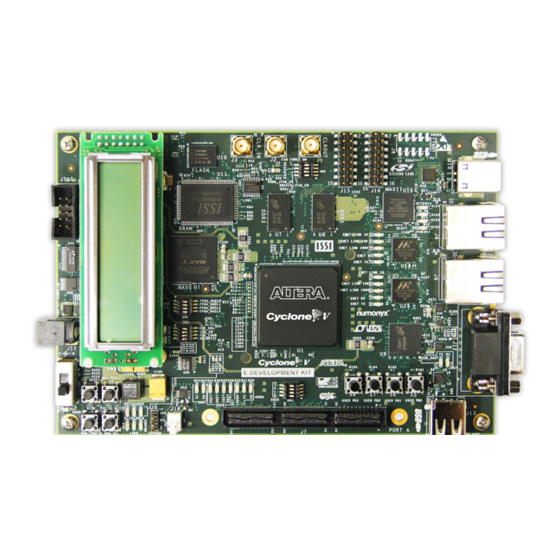
2–2 Chapter 2: Board Components Board Overview Board Overview This section provides an overview of the Cyclone V E FPGA development board, including an annotated board image and component descriptions. Figure 2–1 shows an overview of the board features. Figure 2–1. Overview of the Cyclone V E FPGA Development Board Features... - Page 11 Two 256-MB DDR3 SDRAM with a 16-bit data bus. 512-MB LPDDR 2 SDRAM with 32-bit bus, only 16-bit bus is used on LPDDR2 x 16 memory this board. August 2017 Altera Corporation Cyclone V E FPGA Development Board Reference Manual Arrow.com. Arrow.com. Arrow.com.
-
Page 12: Featured Device: Cyclone V E Fpga
DC input jack. Featured Device: Cyclone V E FPGA The Cyclone V E FPGA development board features a Cyclone V E FPGA 5CEFA7F31I7N device (U1) in a 896-pin FBGA package. For more information about Cyclone V device family, refer to the Cyclone V Device Handbook. -
Page 13: I/O Resources
The Cyclone V E FPGA 5CEFA7F31I7N device has total of 480 user I/Os. Table 2–3 lists the Cyclone V E FPGA I/O pin count and usage by function on the board. Table 2–3. Cyclone V E FPGA I/O Pin Count... - Page 14 Altera Design Store. In the Cyclone V E FPGA Development Kit, under Design Examples, click Cyclone V E FPGA Development Kit Baseline Pinout. Table 2–4. MAX V CPLD 5M2210 System Controller Device Pin-Out (Part 1 of 5)
- Page 15 FPGA partial reconfiguration request FPGA_PR_REQUEST 3.3-V FPGA configuration chip select FPGA_MAX_NCS 2.5-V FSM address bus FSM_A1 2.5-V FSM address bus FSM_A2 August 2017 Altera Corporation Cyclone V E FPGA Development Board Reference Manual Arrow.com. Arrow.com. Arrow.com. Arrow.com. Arrow.com. Arrow.com. Arrow.com. Arrow.com. Arrow.com. Arrow.com.
- Page 16 FSM data bus FSM_D11 2.5-V FSM data bus FSM_D12 2.5-V FSM data bus FSM_D13 2.5-V FSM data bus FSM_D14 Cyclone V E FPGA Development Board August 2017 Altera Corporation Reference Manual Arrow.com. Arrow.com. Arrow.com. Arrow.com. Arrow.com. Arrow.com. Arrow.com. Arrow.com. Arrow.com.
- Page 17 2.5-V Power monitor SPI clock SENSE_SCK 2.5-V Power monitor SPI data in SENSE_SDI 2.5-V Power monitor SPI data out SENSE_SDO August 2017 Altera Corporation Cyclone V E FPGA Development Board Reference Manual Arrow.com. Arrow.com. Arrow.com. Arrow.com. Arrow.com. Arrow.com. Arrow.com. Arrow.com.
-
Page 18: Fpga Configuration
FPGA Programming over Embedded USB-Blaster II This configuration method implements a USB type-B connector (J10), a USB 2.0 PHY device (U18), and an Altera MAX II CPLD EPM570GF100I5N (U16) to allow FPGA configuration using a USB cable. This USB cable connects directly between the USB type-B connector on the board and a USB port of a PC running the Quartus II software. - Page 19 GUI interfaces. Table 2–5 lists the USB 2.0 PHY schematic signal names and their corresponding Cyclone V E FPGA pin numbers. Table 2–5. USB 2.0 PHY Schematic Signal Names and Functions (Part 1 of 2) Board Reference Schematic...
- Page 20 Write strobe for slave FIFO FX2_SLWRN — 3.3-V USB 2.0 PHY wake signal FX2_WAKEUP AA23 3.3-V USB 2.0 PHY 48-MHz interface clock USB_CLK Cyclone V E FPGA Development Board August 2017 Altera Corporation Reference Manual Arrow.com. Arrow.com. Arrow.com. Arrow.com. Arrow.com. Arrow.com. Arrow.com.
-
Page 21: Fpga Programming From Flash Memory
The PFL megafunction is a block of logic that is programmed into an Altera programmable logic device (FPGA or CPLD). The PFL functions as a utility for writing to a compatible flash memory device. This... -
Page 22: Fpga Programming Over External Usb-Blaster
For more information on the following topics, refer to the respective documents: Board Update Portal, PFL design, and flash memory map storage, refer to the ■ Cyclone V E FPGA Development Kit User Guide. PFL megafunction, refer to Parallel Flash Loader Megafunction User Guide. -
Page 23: Fpga Programming Using Epcq
AS mode, resistor rework needs to be done. Configure the MSEL setting using the MSEL DIP switch (SW1) to change the configuration scheme. Figure 2–5 shows the connection between the EPCQ and the Cyclone V E FPGA. Figure 2–5. EPCQ Configuration CCPGM 10 kΩ... -
Page 24: Setup Elements
JTAG settings DIP switch CPU reset push button ■ ■ MAX V reset push button ■ Program configuration push button Program select push button ■ Cyclone V E FPGA Development Board August 2017 Altera Corporation Reference Manual Arrow.com. Arrow.com. Arrow.com. Arrow.com. Arrow.com. Arrow.com. -
Page 25: Board Settings Dip Switch
RESERVED CPU Reset Push Button The CPU reset push button, CPU_RESETn (S4), is an input to the Cyclone V E FPGA DEV_CLRn pin and is an open-drain I/O from the MAX V CPLD System Controller. This push button is the default reset for both the FPGA and CPLD logic. The MAX V CPLD 5M2210 System Controller also drives this push button during power-on-reset (POR). -
Page 26: Max V Reset Push Button
This section describes the board's clock inputs and outputs. On-Board Oscillators The development board include oscillators with a frequency of 50-MHz, 100-MHz, and a programmable oscillator. Cyclone V E FPGA Development Board August 2017 Altera Corporation Reference Manual Arrow.com. Arrow.com. - Page 27 Chapter 2: Board Components 2–19 Clock Circuitry Figure 2–6 shows the default frequencies of all external clocks going to the Cyclone V E FPGA development board. Figure 2–6. Cyclone V E FPGA Development Board Clocks CLK_USB FA-128 SG-310DF 10/100/1000 Cypress...
-
Page 28: Off-Board Clock Input/Output
Board references S5, S6, S7, and S8 are push buttons for controlling the FPGA designs that loads into the Cyclone V E FPGA device. When you press and hold down the switch, the device pin is set to logic 0; when you release the switch, the device pin is set to logic 1. -
Page 29: User-Defined Dip Switch
LEDs from the designs loaded into the Cyclone V E FPGA. Driving a logic 0 on the I/O port turns the LED on while driving a logic 1 turns the LED off. There are no board-specific functions for these LEDs. -
Page 30: Hsmc Leds
Table 2–17 summarizes the character LCD pin assignments. The signal names and directions are relative to the Cyclone V E FPGA device. Table 2–17. Character LCD Pin Assignments, Schematic Signal Names, and Functions Board Cyclone V E FPGA... -
Page 31: Debug Header
Single-ended signal for debug purposes only HEADER_D4 1.5-V Single-ended signal for debug purposes only HEADER_D5 1.5-V Single-ended signal for debug purposes only HEADER_D6 August 2017 Altera Corporation Cyclone V E FPGA Development Board Reference Manual Arrow.com. Arrow.com. Arrow.com. Arrow.com. Arrow.com. Arrow.com. Arrow.com. -
Page 32: Components And Interfaces
Pseudo-differential signals for debug purposes only HEADER_N5 Components and Interfaces This section describes the development board's communication ports and interface cards relative to the Cyclone V E FPGA device. The development board supports the following communication ports: ■ RS-232 Serial UART ■... - Page 33 25-MHz RGMII transmit clock ENETA_XTAL_25MHZ — 2.5-V CMOS Media dependent interface ENETA_MDI_P0 — 2.5-V CMOS Media dependent interface ENETA_MDI_N0 August 2017 Altera Corporation Cyclone V E FPGA Development Board Reference Manual Arrow.com. Arrow.com. Arrow.com. Arrow.com. Arrow.com. Arrow.com. Arrow.com. Arrow.com. Arrow.com.
- Page 34 2.5-V CMOS Media dependent interface ENETB_MDI_N1 — 2.5-V CMOS Media dependent interface ENETB_MDI_P2 — 2.5-V CMOS Media dependent interface ENETB_MDI_N2 Cyclone V E FPGA Development Board August 2017 Altera Corporation Reference Manual Arrow.com. Arrow.com. Arrow.com. Arrow.com. Arrow.com. Arrow.com. Arrow.com. Arrow.com.
-
Page 35: Hsmc
QSH-DP/QTH-DP series. Bank 2 and bank 3 have all the pins populated as done in the QSH/QTH series. Since the Cyclone V E FPGA development board is not a transceiver board, the transceiver pins of the HSMC is not connected to the Cyclone V E FPGA device. - Page 36 LVDS or 2.5-V LVDS RX bit 3n or CMOS bit 19 HSMC_RX_D_N3 AH24 LVDS or 2.5-V LVDS TX bit 4 or CMOS bit 20 HSMC_TX_D_P4 Cyclone V E FPGA Development Board August 2017 Altera Corporation Reference Manual Arrow.com. Arrow.com. Arrow.com.
- Page 37 LVDS or 2.5-V LVDS RX bit 12 or CMOS bit 57 HSMC_RX_D_P12 AH20 LVDS or 2.5-V LVDS TX bit 12n or CMOS bit 58 HSMC_TX_D_N12 August 2017 Altera Corporation Cyclone V E FPGA Development Board Reference Manual Arrow.com. Arrow.com. Arrow.com. Arrow.com.
-
Page 38: Rs-232 Serial Uart
Table 2–24 lists the RS-232 serial UART pin assignments, signal names, and functions. The signal names and types are relative to the Cyclone V E FPGA in terms of I/O setting and direction. Table 2–22. RS-232 Serial UART Schematic Signal Names and Functions... -
Page 39: Usb-Uart
Table 2–23 lists the USB-UART pin assignments, signal names, and functions. The signal names and types are relative to the Cyclone V E FPGA in terms of I/O setting and direction. Table 2–23. USB-UART Schematic Signal Names and Functions... -
Page 40: Memory
Table 2–24 lists the DDR3 pin assignments, signal names, and functions. The signal names and types are relative to the Cyclone V E FPGA in terms of I/O setting and direction. Table 2–24. DDR3 Device Pin Assignments, Schematic Signal Names, and Functions (Part 1 of 4) - Page 41 SSTL Class I Differential 1.5-V Data strobe N byte lane 1 DDR3_DQS_N1 SSTL Class I 1.5-V SSTL Class I On-die termination enable DDR3_ODT August 2017 Altera Corporation Cyclone V E FPGA Development Board Reference Manual Arrow.com. Arrow.com. Arrow.com. Arrow.com. Arrow.com. Arrow.com. Arrow.com.
- Page 42 Data bus byte lane 2 DDR3_DQ22 1.5-V SSTL Class I Data bus byte lane 2 DDR3_DQ23 1.5-V SSTL Class I Data bus byte lane 3 DDR3_DQ24 Cyclone V E FPGA Development Board August 2017 Altera Corporation Reference Manual Arrow.com. Arrow.com. Arrow.com. Arrow.com. Arrow.com.
-
Page 43: Lpddr2 Sdram
Table 2–25 lists the LPDDR2 SDRAM pin assignments, signal names, and functions. The signal names and types are relative to the Cyclone V E FPGA in terms of I/O setting and direction. Table 2–25. LPDDR2 SDRAM Schematic Signal Names and Functions... - Page 44 Data bus byte lane 3 LPDDR2_DQ26 — 1.2-V HSUL Data bus byte lane 3 LPDDR2_DQ27 — 1.2-V HSUL Data bus byte lane 3 LPDDR2_DQ28 Cyclone V E FPGA Development Board August 2017 Altera Corporation Reference Manual Arrow.com. Arrow.com. Arrow.com. Arrow.com. Arrow.com. Arrow.com. Arrow.com.
-
Page 45: Eeprom
I Table 2–26 lists the EEPROM pin assignments, signal names, and functions. The signal names and types are relative to the Cyclone V E FPGA in terms of I/O setting and direction. Table 2–26. EEPROM Schematic Signal Names and Functions... -
Page 46: Synchronous Sram
FSM_D1 2.5-V Data bus FSM_D2 2.5-V Data bus FSM_D3 2.5-V Data bus FSM_D4 2.5-V Data bus FSM_D5 Cyclone V E FPGA Development Board August 2017 Altera Corporation Reference Manual Arrow.com. Arrow.com. Arrow.com. Arrow.com. Arrow.com. Arrow.com. Arrow.com. Arrow.com. Arrow.com. Arrow.com. Arrow.com. -
Page 47: Flash
Table 2–28 lists the flash pin assignments, signal names, and functions. The signal names and types are relative to the Cyclone V E FPGA in terms of I/O setting and direction. Table 2–28. Flash Pin Assignments, Schematic Signal Names, and Functions (Part 1 of 3) - Page 48 FSM_D2 2.5-V Data bus FSM_D3 2.5-V Data bus FSM_D4 2.5-V Data bus FSM_D5 2.5-V Data bus FSM_D6 Cyclone V E FPGA Development Board August 2017 Altera Corporation Reference Manual Arrow.com. Arrow.com. Arrow.com. Arrow.com. Arrow.com. Arrow.com. Arrow.com. Arrow.com. Arrow.com. Arrow.com. Arrow.com.
-
Page 49: Power Supply
65 W. The DC voltage is then stepped down to various power rails used by the board components and installed into the HSMC connectors. An on-board multi-channel analog-to-digital converter (ADC) measures the current for several specific board rails. August 2017 Altera Corporation Cyclone V E FPGA Development Board Reference Manual Arrow.com. Arrow.com. Arrow.com. -
Page 50: Power Distribution System
5.37 V LDO 5.37 V at 0.3 mA FPGA Power Rails Power 20 mA, +/- 5% Monitor Board Main Power Rails LT3009 Cyclone V E FPGA Development Board August 2017 Altera Corporation Reference Manual Arrow.com. Arrow.com. Arrow.com. Arrow.com. Arrow.com. Arrow.com. -
Page 51: Power Measurement
VCCIO7A, VCCIO8A VCCIO5A, VCCIO_1.2V VCC I/O banks 5A and 5B (LPDDR2) VCCIO5B, VCCIO_1.5V VCCIO_4A VCC I/O bank 4A (DDR3) August 2017 Altera Corporation Cyclone V E FPGA Development Board Reference Manual Arrow.com. Arrow.com. Arrow.com. Arrow.com. Arrow.com. Arrow.com. Arrow.com. Arrow.com. Arrow.com. - Page 52 2–44 Chapter 2: Board Components Power Supply Cyclone V E FPGA Development Board August 2017 Altera Corporation Reference Manual Arrow.com. Arrow.com. Arrow.com. Arrow.com. Arrow.com. Arrow.com. Arrow.com. Arrow.com. Arrow.com. Arrow.com. Arrow.com. Arrow.com. Arrow.com. Arrow.com. Arrow.com. Arrow.com. Arrow.com. Arrow.com. Arrow.com. Arrow.com. Arrow.com.
-
Page 53: Chapter 3. Board Components Reference
3. Board Components Reference This chapter describes the Cyclone V E FPGA development board components, the manufacturing information, and the board compliance statements. Board Components Table lists the component reference and manufacturing information of all the components on the development board. -
Page 54: Statement Of China-Rohs Compliance
(EMI) that exceeds the limits established for this equipment. Any EMI caused as the result of modifications to the delivered material is the responsibility of the user. Cyclone V E FPGA Development Board August 2017 Altera Corporation Reference Manual Arrow.com. -
Page 55: Additional Information
Additional Information This chapter provides additional information about the document and Altera. Board Revision History The following table lists the versions of all releases of the Cyclone V E FPGA Development Board. Release Date Version Description New board revision. New device part number—5CEFA7F31I7N. - Page 56 Email Subscription Management Center page of the Altera website, where you can sign up to receive update notifications for Altera documents. The feedback icon allows you to submit feedback to Altera about the document. Methods for collecting feedback vary as appropriate for each document.
Need help?
Do you have a question about the Cyclone V E FPGA and is the answer not in the manual?
Questions and answers