Altera Cyclone III Reference Manual
Hide thumbs
Also See for Cyclone III:
- Reference manual (33 pages) ,
- User manual (34 pages) ,
- Getting started manual (34 pages)
Table of Contents
Advertisement
Quick Links
Download this manual
See also:
User Manual
Advertisement
Table of Contents

Related Manuals for Altera Cyclone III


Summary of Contents for Altera Cyclone III
-
Page 1: Reference Manual
Cyclone III Development Board Reference Manual 101 Innovation Drive San Jose, CA 95134 www.altera.com Document Date: March 2008... - Page 2 Altera Corporation in the U.S. and other countries. All other product or service names are the property of their respective holders. Al- tera products are protected under numerous U.S.
-
Page 3: Table Of Contents
POWER SELECT Rotary Switch ....................2-24 PGM CONFIG SELECT Rotary Switch................... 2-25 Speaker Header (J5) ........................2-26 Clocking Circuitry ..........................2-26 Cyclone III FPGA Clock Inputs..................... 2-26 Cyclone III FPGA Clock Outputs....................2-27 Oscillators ............................2-30 General User Interfaces........................2-30 User-Defined Push Button Switches..................... - Page 4 10/100/1000 Ethernet........................2-47 High Speed Mezzanine Cards ....................... 2-51 On-Board Memory ..........................2-55 DDR2 SDRAM ..........................2-55 SRAM ..............................2-58 Flash Memory ..........................2-62 Power Supply ............................2-65 Power Measurement ..........................2-67 Statement of China-RoHS Compliance ..................... 2-69 Altera Corporation Preliminary...
-
Page 5: About This Manual
Note (1) Technical support www.altera.com/mysupport/ Technical training www.altera.com/training/ Technical training services custrain@altera.com Product literature www.altera.com/literature Product literature services literature@altera.com FTP site ftp.altera.com Note to table: You can also contact your local Altera sales office or sales representative. Altera Corporation Preliminary... -
Page 6: Typographic Conventions
How to Contact Altera Cyclone FPGA Device Handbook Typographic This document uses the typographic conventions shown below. Conventions Visual Cue Meaning Bold Type with Initial Command names, dialog box titles, checkbox options, and dialog box options are Capital Letters shown in bold, initial capital letters. Example: Save As dialog box. -
Page 7: Chapter 1. Overview
FPGA designs that interface with all components of the board. For information on setting up and powering up the Cyclone III development board and using the kit’s demo software, please refer to the Cyclone III Development Kit User Guide. -
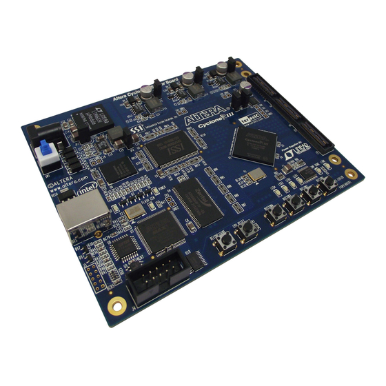
Page 8: Board Component Blocks
Create a Cyclone III FPGA design in one hour ■ View Cyclone III FPGA power measurement examples ■ Design a 32-bit soft processor system inside the Cyclone III FPGA in one hour The Cyclone III development board has the following main features: ■... - Page 9 ● ™ On-board USB-Blaster circuitry using the Quartus II ● Programmer ■ On-board clocking circuitry Two clock oscillators to support Cyclone III device user logic ● • 50-MHz • 125-MHz 80 I/O, 6 clocks, SMBus, and JTAG ● SMA connector for external clock input and output ●...
-
Page 10: Block Diagram
Handling the Board Block Diagram Figure 1–1 shows the functional block diagram of the Cyclone III development board. Figure 1–1. Cyclone III Development Board Block Diagram HSMC Port A HSMC Port B 125 MHz Power XTAL RJ-45 Measure/ Jack Display 2.5V CMOS... -
Page 11: Chapter 2. Board Components
Cyclone III Development Kit documents directory. For information on powering up the development board and installing the demo software, refer to the Cyclone III Development Kit User Guide. Board Overview This section provides an overview of the Cyclone III development board, including an annotated board image and component descriptions. - Page 12 Board Overview Figure 2–1. Top View of the Cyclone III Development Board Table 2–1 describes the components and lists their corresponding board references. Table 2–1. Cyclone III Development Board (Part 1 of 3) Board Reference Type Description Featured Devices FPGA...
- Page 13 Board Components Table 2–1. Cyclone III Development Board (Part 2 of 3) Board Reference Type Description Configuration Status and Setup Elements Device select (DEV_SEL) Sets target device for JTAG signals when using an external jumper ™ USB Blaster or equivalent.
- Page 14 Board Overview Table 2–1. Cyclone III Development Board (Part 3 of 3) Board Reference Type Description SMA clock input SMA connector that allows the provision of an external clock input. SMA clock output SMA connector that allows the provision of an external clock output.
-
Page 15: Featured Fpga (U20)
The Cyclone III Development Kit features the EP3C120F780 device (U20) in a 780-pin BGA package. FPGA (U20) For more information on Cyclone III devices, refer to the Cyclone III Device Handbook. Table 2–2 lists the main Cyclone III device features. -
Page 16: I/O And Clocking Resources
Featured FPGA (U20) Table 2–4. Cyclone III Device Pin Count (Part 2 of 2) Function I/O Type I/O Count Special Pins Vertical bank OCT 2.5 V CMOS 2 Rup, 2 Rdn calibration Passive serial 2.5 V CMOS DATAO, DCLK configuration Ethernet 2.5 V CMOS... -
Page 17: Max Ii Cpld
Board Components Figure 2–2. Cyclone III Device I/O Bank Resources MAX II CPLD The board utilizes an Altera MAX II CPLD for the following purposes: ■ Power-up configuration of the FPGA from flash memory ■ ™ Embedded USB-Blaster core for USB-based configuration of the FPGA ■... - Page 18 I/O Standard Number Direction Signal Name — Input — Input — Output — Input 1.8 V Output clkin_125_en 1.8 V Input clkin_24 1.8 V Output clkin_50_en 1.8 V Input cpu_resetn 2–8 Reference Manual Altera Corporation Cyclone III Development Board March 2008...
- Page 19 1.8 V Output fsa[15] 1.8 V Output fsa[16] 1.8 V Output fsa[17] 1.8 V Output fsa[18] 1.8 V Output fsa[19] 1.8 V Output fsa[2] 1.8 V Output fsa[20] Altera Corporation Reference Manual 2–9 March 2008 Cyclone III Development Board...
- Page 20 1.8 V Bidirectional fsd[22] 1.8 V Bidirectional fsd[23] 1.8 V Bidirectional fsd[24] 1.8 V Bidirectional fsd[25] 1.8 V Bidirectional fsd[26] 1.8 V Bidirectional fsd[27] 1.8 V Bidirectional fsd[28] 2–10 Reference Manual Altera Corporation Cyclone III Development Board March 2008...
- Page 21 — GNDIO — GNDIO — GNDIO — GNDIO — GNDIO — GNDIO — GNDIO — GNDIO — GNDIO — GNDIO — GNDIO — GNDIO — GNDIO — GNDIO — Altera Corporation Reference Manual 2–11 March 2008 Cyclone III Development Board...
- Page 22 2.5 V Input maxgp_jtag_tck 2.5 V Output maxgp_jtag_tdi 2.5 V Input maxgp_jtag_tdo 2.5 V Input maxgp_jtag_tms 1.8 V Input mwatts_mamps 1.8 V Input pgm[0] 1.8 V Input pgm[1] 2–12 Reference Manual Altera Corporation Cyclone III Development Board March 2008...
- Page 23 Input pwr_sel[3] — — RESERVED_INPUT — — RESERVED_INPUT — — RESERVED_INPUT — — RESERVED_INPUT — — RESERVED_INPUT — — RESERVED_INPUT — — RESERVED_INPUT — — RESERVED_INPUT — — RESERVED_INPUT Altera Corporation Reference Manual 2–13 March 2008 Cyclone III Development Board...
- Page 24 2.5 V Bidir usb_phy_fd[1] 2.5 V Bidir usb_phy_fd[10] 2.5 V Bidir usb_phy_fd[11] 2.5 V Bidir usb_phy_fd[12] 2.5 V Bidir usb_phy_fd[13] 2.5 V Bidir usb_phy_fd[14] 2.5 V Bidir usb_phy_fd[15] 2–14 Reference Manual Altera Corporation Cyclone III Development Board March 2008...
- Page 25 Output usb_wr — Power VCCINT — Power VCCINT — Power VCCINT — Power VCCINT — Power VCCINT — Power VCCINT — Power VCCINT — Power VCCINT — Power VCCIO1 Altera Corporation Reference Manual 2–15 March 2008 Cyclone III Development Board...
- Page 26 Table 2–6. MAX II Component Reference and Manufacturing Information Board Manufacturing Manufacturer Description Manufacturer Reference Part Number Web Site 256-pin device in a Altera Corporation EPM2210GF256C3N www.altera.com FineLine Ball Grid Array (FBGA) package 2–16 Reference Manual Altera Corporation Cyclone III Development Board March 2008...
-
Page 27: Configuration, Status, And Setup Elements
The JTAG chain is mastered by the embedded USB Blaster function found in the MAX II device. Only a USB cable is needed to program the Cyclone III FPGA. Any device can be bypassed by using the appropriate switch on the JTAG control DIP switch. - Page 28 Configuration, Status, and Setup Elements Figure 2–4. JTAG Chain with the MAX II Device and the Cyclone III Device The JTAG header can be used with an external USB Blaster cable, or equivalent, to program either the MAX II CPLD or the Cyclone III FPGA.
-
Page 29: Fpga Programming From Flash Memory
Cyclone III FPGA from flash memory. The PFL megafunction reads 16-bit data from the flash memory and converts it to passive serial format. The data is written to the Cyclone III device’s dedicated DCLK and D0 configuration pins at 12 MHz. -
Page 30: Status Elements
Flash Loader with the Quartus II software. ■ Basic flash programming instructions for the development board, refer to the Cyclone III Development User Guide, Appendix A, Programming the Flash Device. Status Elements The development board includes general user, board specific, and HSMC user LEDs. -
Page 31: Power Display
Driven by the Marvell 88E1111 PHY. 1000 Mb Illuminates when Ethernet PHY is using the 1000 Mbps connection speed. Driven by the Marvell 88E1111 PHY. Also connects to Cyclone III FPGA. Duplex Illuminates when Ethernet PHY is both sending and receiving data. Driven by the Marvell 88E1111 PHY. -
Page 32: Setup Elements
SW3 DIP switch allows data to bypass the HSMC interfaces as well as the MAX II CPLD. See “FPGA Programming Over USB” on page 2–17. For information on user-defined DIP switches, refer to “User-Defined DIP Switches” on page 2–32. 2–22 Reference Manual Altera Corporation Cyclone III Development Board March 2008... - Page 33 MAX II Device Control DIP Switch Board reference SW1 is the board settings DIP switch, which controls various features specific to the Cyclone III development board and factory default (board test system) FPGA design: On = logic 0 and off = logic 1.
-
Page 34: System Reset & Configuration Switches
Board reference S5 is the CPU reset push button switch, CPU_RESET, which is an input to both the Cyclone III FPGA and the MAX II CPLD. The CPU_RESET push button is intended to be the master reset signal for... -
Page 35: Power Select Rotary Switch
Note (1) — All 3.3 V power (voltage only), 3.3V Note (1) — All 5.0 V power (voltage only), 5.0V — All 12 V power (voltage only), Note (1) Altera Corporation Reference Manual 2–25 March 2008 Cyclone III Development Board... -
Page 36: Pgm Config Select Rotary Switch
PGM CONFIG SELECT Rotary Switch A 16-position rotary switch, board reference SW5, is used to select the location in flash memory to load the Cyclone III FPGA design. The rotary switch has 16 positions but only the first eight are used. For information on the flash memory locations, refer to Table 2–58 on page... -
Page 37: Clocking Circuitry
P/N pairs. A voltage translator, National Semiconductor part number FXLP34, is located in between the HSMC interfaces and the Cyclone III FPGA to reduce LVTTL to 1.8 V CMOS input levels for clock 0 signals HSMA_CLK_IN0 and HSMB_CLK_IN0. -
Page 38: Cyclone Iii Fpga Clock Outputs
Cyclone III FPGA. Some signals are connected to 1.8 V banks and some are connected to 2.5 V banks. Refer to the Cyclone III Device Handbook for information on voltage output levels. The clock 1 and clock 2 signals from the HSMC interface can be used as LVDS pairs or as eight separate clock signals. - Page 39 Board Components Figure 2–6. Cyclone III FPGA Clock Outputs Table 2–20 shows the clocking parts list. Table 2–20. Cyclone III Development Board Clocking Parts List (Part 1 of 2) Board Manufacturer Description Manufacturer Manufacturer Web Site Reference Part Number 50 MHz LVDS oscillator Pletronics SM5545TEX-50.00M...
-
Page 40: Oscillators
Clocking Circuitry Table 2–20. Cyclone III Development Board Clocking Parts List (Part 2 of 2) Board Manufacturer Description Manufacturer Manufacturer Web Site Reference Part Number 6 MHz crystal Abracon ABL-6.000MHZ-B2 www.abracon.com Corporation 25 MHz crystal oscillator ECS, Inc. ECS-3953C-250-B www.ecsxtal.com... -
Page 41: General User Interfaces
Board reference S5 is the user reset push button switch, CPU_RESETn, which is an input to the Cyclone III device and MAX II CPLD. It is intended to be the master reset signal for the FPGA design loaded into the Cyclone III device. -
Page 42: User-Defined Dip Switches
0 by pushing it to the closed position. There is no board-specific function for these switches. Table 2–25 lists the user DIP switch settings, schematic signal name, and corresponding Cyclone III device’s pin number. Table 2–25. User-Defined DIP Switch Pin-Out (SW6) (Part 1 of 2) Cyclone III Board Reference... -
Page 43: User-Defined Leds
Table 2–27 lists the general user LED reference numbers, schematic signal names, and corresponding Cyclone III device’s pin numbers. Table 2–27. LED Reference Number, Schematic Signal Name, and Cyclone III Device Pin Number (Part 1 LED Board Schematic Signal Cyclone III Device... -
Page 44: Hsmc User-Defined Leds
General User Interfaces Table 2–27. LED Reference Number, Schematic Signal Name, and Cyclone III Device Pin Number (Part 2 LED Board Schematic Signal Cyclone III Device Description I/O Standard Reference Name Pin Number User-defined LED 1.8 V USER_LED5 AC17 User-defined LED 1.8 V... -
Page 45: Ddr2 User-Defined Leds
DDR2TOP_ACTIVE and DDR2BOT_ACTIVE on the silkscreen and are intended to be illuminated when each respective memory channel is being accessed. The LEDs are driven by the Cyclone III device. Table 2–31 lists the DDR2 user-defined LED board reference numbers, schematic signal name, and corresponding Cyclone III device pin numbers. -
Page 46: 7-Segment Displays
SEVEN_SEG_G U30 pin 2 User-defined display signal 1.8 V SEVEN_SEG_DP U30 pin 13 User-defined display signal 1.8 V SEVEN_SEG_SEL1 U30 pin 1 User-defined display select signal 1.8 V SEVEN_SEG_SEL2 2–36 Reference Manual Altera Corporation Cyclone III Development Board March 2008... - Page 47 Table 2–34. 7-Segment Display Component Reference and Manufacturing Information Board Manufacturing Manufacturer Description Manufacturer Reference Part Number Web Site 7-segment, green LED Lumex, Inc. LDQ-M2212R1 www.lumex.com display Altera Corporation Reference Manual 2–37 March 2008 Cyclone III Development Board...
-
Page 48: Lcd Displays
LCM-S01602DSR/C). The LCD has a 14-pin receptacle that mounts directly to the board’s 14-pin header, so it can be easily removed for access to components under the display—or to use the header for debugging or other purposes. 2–38 Reference Manual Altera Corporation Cyclone III Development Board March 2008... - Page 49 Board Components Table 2–36 summarizes the character LCD interface pins. Signal names and directions are relative to the Cyclone III FPGA. For functional descriptions, see Table 2–37. Table 2–36. Character LCD Header I/O Board Schematic Cyclone III Description I/O Standard...
- Page 50 Table 2–38. Character LCD Display Component Reference and Manufacturing Information Board Manufacturing Manufacturer Description Manufacturer Reference Part Number Web Site 2x7 pin, 100 mil, vertical Samtec TSM-107-01-G-DV www.samtec.com header 2x16 character display, Lumex LCM-S01602DSR/C www.lumex.com 5x8 dot matrix 2–40 Reference Manual Altera Corporation Cyclone III Development Board March 2008...
-
Page 51: Graphics Lcd (J13)
LCD write enable 2.5 V LCD_WEn Note to Table 2–39: For the corresponding Cyclone III device pin number, refer to MAX II device pinout tables on the MAX II device literature page, www.altera.com/literature/lit-max2.jsp.<Is this the preferred link?> Altera Corporation Reference Manual 2–41... - Page 52 DC/DC voltage converter negative connection DC/DC voltage converter negative connection DC/DC voltage converter positive connection Power supply for LCD drive V = 1/9-V Power supply for LCD drive V = 2/9-V 2–42 Reference Manual Altera Corporation Cyclone III Development Board March 2008...
- Page 53 Corporation (part number NJU6676), and Figure 2–9 illustrates the functional block diagram of the display driver. For more information, contact Optrex American at www.optrex.com New Japan Radio at www.njr.co.jp/index_e.htm. Altera Corporation Reference Manual 2–43 March 2008 Cyclone III Development Board...
- Page 54 Figure 2–9. Graphics LCD Functional Block Diagram of Display Driver Figure 2–10 is an excerpt from the Optrex data sheet and shows the module interface signals for both read and write transactions. 2–44 Reference Manual Altera Corporation Cyclone III Development Board March 2008...
- Page 55 128x64 graphics module, Optrex America, F-51852GNFQJ-LG-ACN www.optrex.com green LCD Inc. Note to Table 2–41: The Cyclone III development board is shipped with either a blue or green Optrex LED display. Altera Corporation Reference Manual 2–45 March 2008 Cyclone III Development Board...
-
Page 56: Communication Ports & Interface Cards
Communication Ports & Interface Cards Communication This section describes the board’s communication ports and interface cards relative to the Cyclone III device. Ports & Interface The board supports the following communication ports: Cards ■ USB 2.0 MAC/PHY ■ 10/100/1000 Ethernet ■... - Page 57 FIFO data bus read enable 2.5 V CMOS in USB_RDn FIFO data bus write enable 2.5 V CMOS in USB_WR FIFO data bus RX enable 2.5 V CMOS out USB_RXFn Altera Corporation Reference Manual 2–47 March 2008 Cyclone III Development Board...
-
Page 58: 10/100/1000 Ethernet
10/100/1000 Ethernet The 10/100/1000 Ethernet PHY port is provided using a dedicated 10/100/1000 base-T, auto-negotiating Ethernet PHY with reduced Gigabit media independent interface (RGMII) to the FPGA. The target 2–48 Reference Manual Altera Corporation Cyclone III Development Board March 2008... - Page 59 I/O standard for the Ethernet PHY interface I/O. The signal names and type are relative to the Cyclone III device, i.e., the I/O setting and direction. Table 2–44. Ethernet PHY Interface I/O (Part 1 of 2)
- Page 60 GTX_CLK. ± ENET_RX_CLK RX_CLK 125 MHz, 25 MHz, or 2.5 MHz receive clock tolerance derived from the received data stream and based on the selected speed. 2–50 Reference Manual Altera Corporation Cyclone III Development Board March 2008...
-
Page 61: High Speed Mezzanine Cards
JTAG, SMBus, clock outputs and inputs, as well as power for compatible HSMC cards. The HSMC is an Altera-developed specification, which allows users to expand the functionality of the development board through the addition of daughter cards (HSMC cards). - Page 62 QSH-DP/QTH-DP series. Bank 2 and Bank 3 have all of the pins populated as done in the QSH/QTH series. The Cyclone III development board does not use Bank 1 transceiver signals intended for clock-data-recover (CDR) applications such as PCI Express and Rapid I/O.
- Page 63 HSMC Port A interface signal names, descriptions, and I/O standard. Signal names and directions are relative to the Cyclone III FPGA, which is the HSMC host. Table 2–47. HSMC Port A Interface Signal Names, Descriptions, and Type (Part 1 of 4)
- Page 64 LVDS RX 10n or CMOS I/O data bit 51 LVDS or 2.5 V HSMA_RX_N10 J8 pin 119 LVDS TX 11p or CMOS I/O data bit 52 LVDS or 2.5 V HSMA_TX_P11 2–54 Reference Manual Altera Corporation Cyclone III Development Board March 2008...
- Page 65 LVDS or CMOS clock in LVDS HSMA_CLK_IN_P2 J8 pin 157 LVDS or CMOS clock out 2.5 V HSMA_CLK_OUT_N2 J8 pin 158 LVDS or CMOS clock in 2.5 V HSMA_CLK_IN_N2 Altera Corporation Reference Manual 2–55 March 2008 Cyclone III Development Board...
- Page 66 HSMC Port B interface signal names, descriptions, and I/O standard. Signal names and directions are relative to the Cyclone III FPGA, which is the HSMC host. Table 2–48. HSMC Port B Interface Signal Names, Descriptions, and Type (Part 1 of 4)
- Page 67 LVDS RX 8n or CMOS I/O data bit 43 LVDS or 2.5 V HSMB_RX_N8 J9 pin 107 LVDS TX 9p or CMOS I/O data bit 44 LVDS or 2.5 V HSMB_TX_N9 Altera Corporation Reference Manual 2–57 March 2008 Cyclone III Development Board...
- Page 68 LVDS RX 14n or CMOS I/O data bit 67 LVDS or 2.5 V HSMB_RX_N14 J9 pin 143 LVDS RX 15p or CMOS I/O data bit 68 LVDS or 2.5 V HSMB_TX_P15 2–58 Reference Manual Altera Corporation Cyclone III Development Board March 2008...
- Page 69 Table 2–49. HSMC Power Supply Minimum Current Voltage Minimum Wattage From Host 12 V 1.0A 12.0 W 3.3 V 2.0A 6.6 W Altera Corporation Reference Manual 2–59 March 2008 Cyclone III Development Board...
-
Page 70: On-Board Memory
TOP and the other is referred to as BOT (bottom), as they connect to the respective Cyclone III device edges. The interface is comprised of four x16 devices for the 64-bit datapath, and a single x8 device for the ECC bits for a total of 5 devices (3 to TOP, 2 to BOT). - Page 71 50 ohms to match the trace impedance of the signals on the board. Clocks are terminated using a single 100 ohm resistor across each P/N pair. Altera recommends using the 50 ohm OCT on the FPGA for data, and the 10 mA setting for the address and control pins. The DDR2 devices should use the reduced drive strength setting available as a register option.
- Page 72 DDR2_DQ30 U25 pin B9 Data 31 SSTL18 Class 1 DDR2_DQ31 AD10 U11 pin G8 Data 32 SSTL18 Class 1 DDR2_DQ32 U11 pin G2 Data 33 SSTL18 Class 1 DDR2_DQ33 2–62 Reference Manual Altera Corporation Cyclone III Development Board March 2008...
- Page 73 SSTL18 Class 1 DDR2_DQ60 U12 pin D9 Data 61 SSTL18 Class 1 DDR2_DQ61 U12 pin B1 Data 62 SSTL18 Class 1 DDR2_DQ62 U12 pin B9 Data 63 SSTL18 Class 1 DDR2_DQ63 Altera Corporation Reference Manual 2–63 March 2008 Cyclone III Development Board...
- Page 74 Bottom address 5 SSTL18 Class 1 DDR2BOT_A5 U25, U26 pin N7 Bottom address 6 SSTL18 Class 1 DDR2BOT_A6 AD12 U25, U26 pin P2 Bottom address 7 SSTL18 Class 1 DDR2BOT_A7 2–64 Reference Manual Altera Corporation Cyclone III Development Board March 2008...
- Page 75 U13 pin J8 U11, U12 pin N3, Top address 5 SSTL18 Class 1 DDR2TOP_A5 U13 pin J3 U11, U12 pin N7, Top address 6 SSTL18 Class 1 DDR2TOP_A6 U13 pin J7 Altera Corporation Reference Manual 2–65 March 2008 Cyclone III Development Board...
- Page 76 Description Manufacturer Reference Part Number Web Site U11, U12, DDR2 SDRAM 34M x16 Micron Technology, MT47H32M16CC-3:B www.micron.com U25, U26 Inc. DDR2 SDRAM 32M x8 Micron Technology, MT47H32M8BP-3:B www.micron.com Inc. 2–66 Reference Manual Altera Corporation Cyclone III Development Board March 2008...
-
Page 77: Sram
SRAM. Table 2–53 lists the SRAM interface signal name, description, and I/O standard. Signal names and type are relative to the Cyclone III device, i.e., I/O setting and direction. Table 2–53. SRAM Interface I/O (Part 1 of 3) Cyclone III... - Page 78 1.8 V FSD14 U23 pin G1 Data bit 15 1.8 V FSD15 U24 pin B6 Data bit 16 1.8 V FSD16 U24 pin C5 Data bit 17 1.8 V FSD17 2–68 Reference Manual Altera Corporation Cyclone III Development Board March 2008...
- Page 79 For asynchronous accesses, each of the two devices has its own WAIT pin wired to the Cyclone III device. For Samsung SRAM pin definitions, data sheet, and other related documentation, refer to the Samsung website at www.samsung.com.
- Page 80 Latency set (A11:A10:A9) 4(0:0:1) 2(1:0:0) 5(0:1:0) 3(0:0:0) 7(1:0:1) 4(0:0:1) Read latency (min) 3/5th First read data fetch clock 3rd/5th 4th/6th 5th/8th Write latency (min) First write data loading clock 3rd 2–70 Reference Manual Altera Corporation Cyclone III Development Board March 2008...
- Page 81 Board Components Figures 2–15 2–16 show the Samsung device read and write access waveforms. Figure 2–15. SRAM Read Timing Waveforms Figure 2–16. SRAM Write Timing Waveforms Altera Corporation Reference Manual 2–71 March 2008 Cyclone III Development Board...
-
Page 82: Flash Memory
The flash device is part of a shared bus with connectivity to the MAX II CPLD as well as the SRAM memory, which is called the FSM bus. All three devices use 1.8 V CMOS signaling. Altera recommends using the 50 ohm OCT setting on the FPGA. The flash does not have a drive strength setting. - Page 83 1.8 V FSD1 U31 pin E4 Data bit 2 1.8 V FSD2 U31 pin H4 Data bit 3 1.8 V FSD3 U31 pin H5 Data bit 4 1.8 V FSD4 Altera Corporation Reference Manual 2–73 March 2008 Cyclone III Development Board...
- Page 84 FSD15 Note to Table 2–56: For the corresponding Cyclone III device pin number, refer to MAX II device pinout tables on the MAX II device literature page, www.altera.com/literature/lit-max2.jsp.<Is this the preferred link?> Table 2–57 defines the flash memory map, and lists the signals required for flash memory.
- Page 85 Description I/O Standard Ground Ground Cyclone III device I/O totals: 29 1.8 V CMOS I/O pins Table 2–58 shows the flash device memory map on the Cyclone III devel- opment board. The memory provides non-volatile storage for a mini- mum of eight FPGA bit streams, as well as various settings data used for on-board devices such as Ethernet TCP/IP defaults, PFL configuration bits, and data on the board itself.
- Page 86 Spansion flash board reference and manufacturing information. Table 2–61. Spansion Flash Manufacturing Information Board Manufacturer Part Manufacturer Description Manufacturer Reference Number Web Site 64 MB of flash Spansion LLC S29GL512N11FFIV1 www.spansion.com memory 2–76 Reference Manual Altera Corporation Cyclone III Development Board March 2008...
-
Page 87: Power Supply
“POWER SELECT Rotary Switch” on page 2–25. Regulator inefficiencies and sharing are reflected in the currents shown. Altera Corporation Reference Manual 2–77 March 2008 Cyclone III Development Board... - Page 88 Power Supply Figure 2–17. Power Distribution System 2–78 Reference Manual Altera Corporation Cyclone III Development Board March 2008...
-
Page 89: Power Measurement
The column Schematic Signal Name lists the power rail being measured, and the power pins/devices attached to the power rail are listed in the Power Pin Name and Description columns. Altera Corporation Reference Manual 2–79 March 2008 Cyclone III Development Board... -
Page 90: Statement Of China-Rohs Compliance
X* indicates that the concentration of the hazardous substance of at least one of all homogeneous materials in the parts is above the relevant threshold of the SJ/T11363-2006 standard, but it is exempted by EU RoHS. 2–80 Reference Manual Altera Corporation Cyclone III Development Board March 2008... - Page 91 Mouser Electronics Authorized Distributor Click to View Pricing, Inventory, Delivery & Lifecycle Information: Terasic K0034 K0035...
Need help?
Do you have a question about the Cyclone III and is the answer not in the manual?
Questions and answers