Table of Contents
Advertisement
Quick Links
Download this manual
See also:
User Manual
Advertisement
Table of Contents

Related Manuals for Altera Cyclone V GX FPGA


Summary of Contents for Altera Cyclone V GX FPGA
- Page 1 Cyclone V GX FPGA Development Board Reference Manual Cyclone V GX FPGA Development Board Reference Manual 101 Innovation Drive San Jose, CA 95134 www.altera.com MNL-01072-1.2 Feedback Subscribe...
- Page 2 © 2013 Altera Corporation. All rights reserved. ALTERA, ARRIA, CYCLONE, HARDCOPY, MAX, MEGACORE, NIOS, QUARTUS and STRATIX words and logos are trademarks of Altera Corporation and registered in the U.S. Patent and Trademark Office and in other countries. All other words and logos identified as trademarks or service marks are the property of their respective holders as described at www.altera.com/common/legal.html.
-
Page 3: Table Of Contents
Featured Device: Cyclone V GX FPGA ........ - Page 4 How to Contact Altera ........
-
Page 5: Chapter 1. Overview
The Cyclone V GX FPGA development board provides a hardware platform for developing and prototyping low-power, high-performance, and logic-intensive designs using Altera’s Cyclone V GX FPGA device. The board provides a wide range of peripherals and memory interfaces to facilitate the development of Cyclone V GX designs. -
Page 6: Board Component Blocks
1–2 Chapter 1: Overview Board Component Blocks Board Component Blocks The development board features the following major component blocks: One Cyclone V GX FPGA (5CGXFC7D6F31C7NES) in a 896-pin FineLine BGA ■ (FBGA) package 150,000 LEs ■ 136,880 adaptive logic modules (ALMs) ■... - Page 7 General user DIP switch ■ ■ Power supply 14–20-V (laptop) DC input ■ PCI Express edge connector ■ ■ Mechanical PCI Express card standard size (6.600" x 4.199") ■ May 2013 Altera Corporation Cyclone V GX FPGA Development Board Reference Manual...
-
Page 8: Development Board Block Diagram
1–4 Chapter 1: Overview Development Board Block Diagram Development Board Block Diagram Figure 1–1 shows a block diagram of the Cyclone V GX FPGA development board. Figure 1–1. Cyclone V GX FPGA Development Board Block Diagram LVDS/Single-Ended 128-MB DDR3 Type-B Embedded USB 2.0... -
Page 9: Statement Of China-Rohs Compliance
2. Board Components This chapter introduces the major components on the Cyclone V GX FPGA development board. Figure 2–1 illustrates the component locations and Table 2–1 provides a brief description of all component features of the board. A complete set of schematics, a physical layout database, and GERBER files for the development board reside in the Cyclone V GX FPGA development kit documents directory. -
Page 10: Chapter 2. Board Components
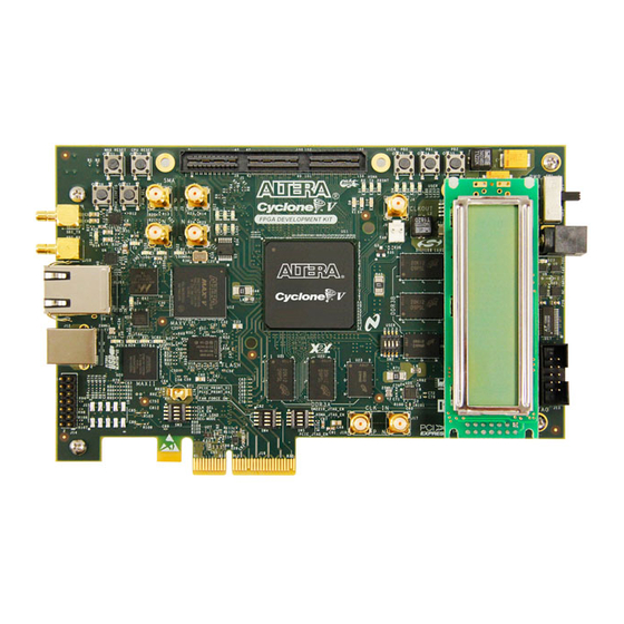
2–2 Chapter 2: Board Components Board Overview Board Overview This section provides an overview of the Cyclone V GX FPGA development board, including an annotated board image and component descriptions. Figure 2–1 shows an overview of the board features. Figure 2–1. Overview of the Cyclone V GX FPGA Development Board Features... - Page 11 Four user LEDs. Illuminates when driven low. User DIP switch Quad user DIP switches. When the switch is ON, a logic 0 is selected. CPU reset push button Reset the FPGA logic. May 2013 Altera Corporation Cyclone V GX FPGA Development Board Reference Manual...
- Page 12 HSMC specification. RJ-45 connector which provides a 10/100/1000 Ethernet connection Gigabit Ethernet port via a Marvell 88E1111 PHY and the FPGA-based Altera Triple Speed Ethernet MegaCore function in RGMII mode. Video and Display Ports Connector that interfaces to a provided 16 character × 2 line LCD Character LCD module along with two standoffs.
-
Page 13: Featured Device: Cyclone V Gx Fpga
Featured Device: Cyclone V GX FPGA Featured Device: Cyclone V GX FPGA The Cyclone V GX FPGA development board features a Cyclone V GX 5CGXFC7D6F31C7NES device (U11) in a 896-pin FBGA package. For more information about Cyclone V device family, refer to the Cyclone V Device Handbook. -
Page 14: Max V Cpld 5M2210 System Controller
2–6 Chapter 2: Board Components MAX V CPLD 5M2210 System Controller MAX V CPLD 5M2210 System Controller The board utilizes the 5M2210 System Controller, an Altera MAX V CPLD, for the following purposes: ■ FPGA configuration from flash ■ Power measurement ■... - Page 15 FPGA configuration ready FPGA_NSTATUS 2.5-V FPGA partial reconfiguration done FPGA_PR_DONE 2.5-V FPGA partial reconfiguration error FPGA_PR_ERROR 2.5-V FPGA partial reconfiguration ready FPGA_PR_READY 2.5-V FPGA partial reconfiguration request FPGA_PR_REQUEST May 2013 Altera Corporation Cyclone V GX FPGA Development Board Reference Manual...
- Page 16 FSM data bus FSM_D6 2.5-V FSM data bus FSM_D7 2.5-V FSM data bus FSM_D8 2.5-V FSM data bus FSM_D9 2.5-V FSM data bus FSM_D10 2.5-V FSM data bus FSM_D11 Cyclone V GX FPGA Development Board May 2013 Altera Corporation Reference Manual...
- Page 17 Flash memory PGM select indicator 2 PGM_LED2 2.5-V Toggles the PGM_LED[2:0] LED sequence PGM_SEL 2.5-V SDI data transmission fault SDI_FAULT 2.5-V SDI equalization bypass SDI_RX_BYPASS 2.5-V SDI receive enable SDI_RX_EN May 2013 Altera Corporation Cyclone V GX FPGA Development Board Reference Manual...
-
Page 18: Fpga Configuration
USB_CLK FPGA Configuration This section describes the FPGA, flash memory, and MAX V CPLD 5M2210 System Controller device programming methods supported by the Cyclone V GX FPGA development board. The Cyclone V GX development board supports the following three configuration methods: ■... -
Page 19: Fpga Programming Over Embedded Usb-Blaster
FPGA Programming over Embedded USB-Blaster This configuration method implements a USB type-B connector (J12), a USB 2.0 PHY device (U16), and an Altera MAX II CPLD EPM240M100C4N (U20) to allow FPGA configuration using a USB cable. This USB cable connects directly between the USB type-B connector on the board and a USB port of a PC running the Quartus II software. - Page 20 USB 2.0 PHY serial clock FX2_SCL — 3.3-V USB 2.0 PHY serial data FX2_SDA — 3.3-V Read strobe for slave FIFO FX2_SLRDN — 3.3-V Write strobe for slave FIFO FX2_SLWRN Cyclone V GX FPGA Development Board May 2013 Altera Corporation Reference Manual...
-
Page 21: Fpga Programming From Flash Memory
The PFL megafunction is a block of logic that is programmed into an Altera programmable logic device (FPGA or CPLD). The PFL functions as a utility for writing to a compatible flash memory device. This... -
Page 22: Fpga Programming Over External Usb-Blaster
10 kΩ For more information on the following topics, refer to the respective documents: Board Update Portal, PFL design, and flash memory map storage, refer to the ■ Cyclone V GX FPGA Development Kit User Guide. ■ PFL megafunction, refer to Parallel Flash Loader Megafunction User Guide. -
Page 23: Status Elements
SDI RX port. Driven by the SDI cable equalizer. Green LED. Illuminates when HSMC port A has a board or cable 3.3-V plugged-in such that pin 160 becomes grounded. Driven by the HSMA_PRSNTn add-in card. May 2013 Altera Corporation Cyclone V GX FPGA Development Board Reference Manual... -
Page 24: Setup Elements
JTAG Chain Control DIP Switch The JTAG chain control DIP switch (SW5) either remove or include devices in the active JTAG chain. The Cyclone V GX FPGA is always in the JTAG chain. Table 2–9 lists the switch controls and its descriptions. -
Page 25: Pci Express Link Width Dip Switch
Controller. This push button toggles the PGM_LED[2:0]sequence that selects which location in the flash memory is used to configure the FPGA. Refer to Table 2–6 for the PGM_LED[2:0] sequence definitions. May 2013 Altera Corporation Cyclone V GX FPGA Development Board Reference Manual... -
Page 26: Clock Circuitry
148.50-MHz, and a quad-clock programmable oscillator. Figure 2–5 shows the default frequencies of all external clocks going to the Cyclone V GX FPGA development board. Figure 2–5. Cyclone V GX FPGA Development Board Clocks IDT5T9306 LVPECL Clock Fan-Out Clock Input... -
Page 27: Off-Board Clock Input/Output
LVDS input from the installed HSMC cable or Samtec HSMC board. Can also support 2x LVTTL inputs. LVDS/LVTTL HSMA_CLK_IN_N2 LVDS PCIE_REFCLK_P PCI Express LVDS input from the PCI Express edge connector. Edge HCSL PCIE_REFCLK_N May 2013 Altera Corporation Cyclone V GX FPGA Development Board Reference Manual... -
Page 28: General User Input/Output
FPGA input control. When the switch is in the OFF position, a logic 1 is selected. When the switch is in the ON position, a logic 0 is selected. There are no board-specific functions for this switch. Cyclone V GX FPGA Development Board May 2013 Altera Corporation Reference Manual... -
Page 29: User-Defined Leds
Table 2–17. HSMC LED Schematic Signal Names and Functions Schematic Cyclone V GX Board Reference I/O Standard Description Signal Name Pin Number 2.5-V HSMA_RX_LED User-defined LEDs AB26 2.5-V HSMA_TX_LED May 2013 Altera Corporation Cyclone V GX FPGA Development Board Reference Manual... -
Page 30: Pci Express Leds
LCD_DATA5 2.5-V LCD data bus LCD_DATA6 2.5-V LCD data bus LCD_DATA7 2.5-V LCD data or command select LCD_D_Cn 2.5-V LCD write enable LCD_WEn 2.5-V LCD chip select LCD_CSn Cyclone V GX FPGA Development Board May 2013 Altera Corporation Reference Manual... -
Page 31: Debug Header
Single-ended signal for debug purposes only DEBUG_HDR6 1.5-V Single-ended signal for debug purposes only DEBUG_HDR2 1.5-V Single-ended signal for debug purposes only DEBUG_HDR9 — 1.5-V Test signal SECURITY_CPLD_MRn May 2013 Altera Corporation Cyclone V GX FPGA Development Board Reference Manual... -
Page 32: Components And Interfaces
SDI video output/input PCI Express The Cyclone V GX FPGA development board is designed to fit entirely into a PC motherboard with a ×4 PCI Express slot that can accommodate a full height long form factor add-in card. This interface uses the Cyclone V GX's PCI Express hard IP block, saving logic resources for the user logic application. - Page 33 2.5-V SMB clock PCIE_SMBCLK 2.5-V SMB data PCIE_SMBDAT 1.5-V PCML Transmit bus PCIE_TX_P0 1.5-V PCML Transmit bus PCIE_TX_N0 1.5-V PCML Transmit bus PCIE_TX_P1 1.5-V PCML Transmit bus PCIE_TX_N1 May 2013 Altera Corporation Cyclone V GX FPGA Development Board Reference Manual...
-
Page 34: 10/100/1000 Ethernet
10/100/1000 Ethernet The development board supports 10/100/1000 base-T Ethernet using an external Marvell 88E1111 PHY and Altera Triple-Speed Ethernet MegaCore MAC function. The PHY-to-MAC interface employs a RGMII interface. The MAC function must be provided in the FPGA for typical networking applications. -
Page 35: Hsmc
SPI4.2 interface (17 LVDS channels), three input and output clocks, as well as JTAG and SMB signals. The LVDS channels can be used for CMOS signaling or LVDS. The HSMC is an Altera-developed open specification, which allows you to expand the functionality of the development board through the addition of daughtercards (HSMCs). - Page 36 1.5-V PCML Transceiver TX bit 2 HSMA_TX_P2 1.5-V PCML Transceiver RX bit 2 HSMA_RX_P2 1.5-V PCML Transceiver TX bit 2n HSMA_TX_N2 1.5-V PCML Transceiver RX bit 2n HSMA_RX_N2 Cyclone V GX FPGA Development Board May 2013 Altera Corporation Reference Manual...
- Page 37 LVDS or 2.5-V LVDS TX bit 4 or CMOS bit 20 HSMA_TX_D_P4 LVDS or 2.5-V LVDS RX bit 4 or CMOS bit 21 HSMA_RX_D_P4 LVDS or 2.5-V LVDS TX bit 4n or CMOS bit 22 HSMA_TX_D_N4 May 2013 Altera Corporation Cyclone V GX FPGA Development Board Reference Manual...
- Page 38 LVDS or 2.5-V LVDS RX bit 12n or CMOS bit 59 HSMA_RX_D_N12 LVDS or 2.5-V LVDS TX bit 13 or CMOS bit 60 HSMA_TX_D_P13 LVDS or 2.5-V LVDS RX bit 13 or CMOS bit 61 HSMA_RX_D_P13 Cyclone V GX FPGA Development Board May 2013 Altera Corporation Reference Manual...
-
Page 39: Sdi Video Output/Input
SMPTE 424M, SMPTE 292M Faster SMPTE 259M Slower For more information about the application circuit of the cable driver, refer to the cable driver data sheet in www.national.com. May 2013 Altera Corporation Cyclone V GX FPGA Development Board Reference Manual... - Page 40 SDI Adaptive Cable Equalizer 1.0 μF 75 Ω Coaxial Cable To FPGA 1.0 μF 5.6 nH 75 Ω 37.4 Ω MUTE MUTE BYPASS MUTE MUTE BYPASS 1.0 μF Cyclone V GX FPGA Development Board May 2013 Altera Corporation Reference Manual...
-
Page 41: Memory
With a soft memory controller, this memory interface runs at a target frequency of 333 MHz for a maximum theoretical bandwidth of over 21.31 Gbps. The maximum frequency for this DDR3 device is 667 MHz with a CAS latency of 9. May 2013 Altera Corporation Cyclone V GX FPGA Development Board Reference Manual... - Page 42 Data bus byte lane 0 DDR3A_DQ6 AF14 1.5-V SSTL Class I Data bus byte lane 0 DDR3A_DQ7 AK17 1.5-V SSTL Class I Data bus byte lane 1 DDR3A_DQ8 Cyclone V GX FPGA Development Board May 2013 Altera Corporation Reference Manual...
- Page 43 Bank address bus DDR3A_BA0 AH10 1.5-V SSTL Class I Bank address bus DDR3A_BA1 AJ10 1.5-V SSTL Class I Bank address bus DDR3A_BA2 1.5-V SSTL Class I Row address select DDR3A_CASN May 2013 Altera Corporation Cyclone V GX FPGA Development Board Reference Manual...
- Page 44 DDR3A_ZQ2 DDR3 x8 (U23) AJ12 1.5-V SSTL Class I Address bus DDR3A_A0 AK12 1.5-V SSTL Class I Address bus DDR3A_A1 AH11 1.5-V SSTL Class I Address bus DDR3A_A2 Cyclone V GX FPGA Development Board May 2013 Altera Corporation Reference Manual...
- Page 45 1.5-V SSTL Class I Row address select DDR3A_RASN AK21 1.5-V SSTL Class I Reset DDR3A_RESETN 1.5-V SSTL Class I Write enable DDR3A_WEN — 1.5-V SSTL Class I ZQ impedance calibration DDR3A_ZQ05 May 2013 Altera Corporation Cyclone V GX FPGA Development Board Reference Manual...
- Page 46 1.5-V SSTL Class I Data bus byte lane 0 DDR3B_DQ6 1.5-V SSTL Class I Data bus byte lane 0 DDR3B_DQ7 1.5-V SSTL Class I Data bus byte lane 1 DDR3B_DQ8 Cyclone V GX FPGA Development Board May 2013 Altera Corporation Reference Manual...
- Page 47 Bank address bus DDR3B_BA0 1.5-V SSTL Class I Bank address bus DDR3B_BA1 1.5-V SSTL Class I Bank address bus DDR3B_BA2 1.5-V SSTL Class I Row address select DDR3B_CASN May 2013 Altera Corporation Cyclone V GX FPGA Development Board Reference Manual...
- Page 48 ZQ impedance calibration DDR3B_ZQ2 DDR3 x8 (U19) 1.5-V SSTL Class I Address bus DDR3B_A0 1.5-V SSTL Class I Address bus DDR3B_A1 AA29 1.5-V SSTL Class I Address bus DDR3B_A2 Cyclone V GX FPGA Development Board May 2013 Altera Corporation Reference Manual...
- Page 49 1.5-V SSTL Class I Row address select DDR3B_RASN AB27 1.5-V SSTL Class I Reset DDR3B_RESETN 1.5-V SSTL Class I Write enable DDR3B_WEN — 1.5-V SSTL Class I ZQ impedance calibration DDR3B_ZQ05 May 2013 Altera Corporation Cyclone V GX FPGA Development Board Reference Manual...
-
Page 50: Synchronous Sram
2.5-V Address bus FSM_A21 2.5-V Data bus FSM_D0 2.5-V Data bus FSM_D1 2.5-V Data bus FSM_D2 2.5-V Data bus FSM_D3 2.5-V Data bus FSM_D4 2.5-V Data bus FSM_D5 Cyclone V GX FPGA Development Board May 2013 Altera Corporation Reference Manual... -
Page 51: Flash
Table 2–32. Flash Pin Assignments, Schematic Signal Names, and Functions (Part 1 of 3) Board Cyclone V GX Schematic Signal Name I/O Standard Description Reference (U18) Pin Number 2.5-V Address valid FLASH_ADVN 2.5-V Chip enable FLASH_CEN May 2013 Altera Corporation Cyclone V GX FPGA Development Board Reference Manual... - Page 52 2.5-V Data bus FSM_D0 2.5-V Data bus FSM_D1 2.5-V Data bus FSM_D2 2.5-V Data bus FSM_D3 2.5-V Data bus FSM_D4 2.5-V Data bus FSM_D5 2.5-V Data bus FSM_D6 Cyclone V GX FPGA Development Board May 2013 Altera Corporation Reference Manual...
-
Page 53: Power Supply
Laptop-style DC input 15.0 25-W PCI Express edge connector 12.0 75-W PCI Express edge connector 12.0 An on-board multi-channel analog-to-digital converter (ADC) measures the current for several specific board rails. May 2013 Altera Corporation Cyclone V GX FPGA Development Board Reference Manual... -
Page 54: Power Distribution System
(115 mA) +/- 5% LTC3025-1 1.0 V LDO Ethernet PHY (304 mA) +/- 5% TPS5110DGQ 0.75 V LDO DDR3 VTT (739 mA) +/- 5% Con Cell FPGA VCCBAT Cyclone V GX FPGA Development Board May 2013 Altera Corporation Reference Manual... -
Page 55: Power Measurement
VCC I/O banks 3, 7, and 8 VCCIO_7A, VCCIO_8A VCCIO_6A, VCCIO_5B, C5_VCCIO_1.5V VCCIO bank (DDR3) VCCIO_4A, VCCIO_3B C5_VCCBAT VCCBAT Battery power C5_VCCH_GXBL VCCH_GXB XCVR block level transmit buffers May 2013 Altera Corporation Cyclone V GX FPGA Development Board Reference Manual... -
Page 56: Statement Of China-Rohs Compliance
(2) X* indicates that the concentration of the hazardous substance of at least one of all homogeneous materials in the parts is above the relevant threshold of the SJ/T11363-2006 standard, but it is exempted by EU RoHS. Cyclone V GX FPGA Development Board May 2013 Altera Corporation... -
Page 57: Chapter 3. Board Components Reference
3. Board Components Reference This chapter lists the component reference and manufacturing information of all the components on the Cyclone V GX FPGA development board. Table 3–1. Component Reference and Manufacturing Information Board Manufacturing Manufacturer Component Manufacturer Reference Part Number... - Page 58 MT41J128M8 www.micron.com 1024K×18 bit 18-MB synchronous Integrated Silicon IS61VPS102418A- www.issi.com SRAM Solution, Inc. 250TQL 512-MB synchronous flash Numonyx PC28F512P30BF www.numonyx.com 16-channel differential 24-bit ADC Linear Technology LTC2418CGN#PBF www.linear.com Cyclone V GX FPGA Development Board May 2013 Altera Corporation Reference Manual...
-
Page 59: Additional Information
(software licensing) Email authorization@altera.com Note to Table: (1) You can also contact your local Altera sales office or sales representative. Typographic Conventions The following table shows the typographic conventions this document uses. Visual Cue Meaning Indicate command names, dialog box titles, dialog box options, and other GUI Bold Type with Initial Capital labels. - Page 60 Email Subscription Management Center page of the Altera website, where you can sign up to receive update notifications for Altera documents. The feedback icon allows you to submit feedback to Altera about the document. Methods for collecting feedback vary as appropriate for each document.
Need help?
Do you have a question about the Cyclone V GX FPGA and is the answer not in the manual?
Questions and answers