Table of Contents
Advertisement
Quick Links
Advertisement
Table of Contents

Related Manuals for Altera CLR-HSMC


Summary of Contents for Altera CLR-HSMC
-
Page 2: Table Of Contents
CONTENTS INTRODUCTION CHAPTER 1 ..........................2 1.1 Features ..................................2 1.2 Getting Help ................................3 ARCHITECTURE & CONFIGURATION CHAPTER 2 ..................4 2.1 Block Diagram ................................5 2.2 Connectivity ................................7 PIN DESCRIPTION CHAPTER 3 ........................... 10 3.1 HSMC Expansion Connector .......................... -
Page 3: Chapter 1 Introduction
HSMC/HSTC carrier such as DE4, DE3 and DE2-115. Figure 1-1 shows the photo of the CLR-HSMC board. The important features are listed below: Support of standard Camera Link modes (base, medium, dual base assembly) Serial Communication with camera ... -
Page 4: Getting Help
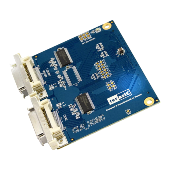
Figure 1-1 Picture of the CLR-HSMC Board Here are some places to get help if you encounter any problem: Email to support@terasic.com Taiwan & China: +886-3-550-8800 Korea : +82-2-512-7661 Japan: +81-428-77-7000... -
Page 5: Chapter 2 Architecture & Configuration
Chapter 2 Architecture & Configuration This chapter describes the architecture and configuration of the CLR-HSMC board including block diagram and components. Figure 2-1 The CLR-HSMC Board PCB and Component Diagram A photograph of the CLR-HSMC is shown in Figure 2-1 Figure 2-2 . -
Page 6: Block Diagram
National Semiconductor DS90LV047A for LVDS to LVTTL adapting of control signals. (U5, National Semiconductor DS90LV019 for LVDS to LVTTL adapting of serial control signals. (U4, U6) Figure 2-3 shows the block diagram of the CLR-HSMC board in base mode configuration. - Page 7 Figure 2-3 Block Diagram of the CLR-HSMC Board (Base Mode) Figure 2-4 shows the block diagram of the CLR-HSMC board in medium mode configuration. Figure 2-4 Block Diagram of the CLR-HSMC Board (Medium Mode)
-
Page 8: Connectivity
Figure 2-5 shows the block diagram of the CLR-HSMC board in dual-base mode configuration. Figure 2-5 Block Diagram of the CLR-HSMC Board (Dual-base Mode) The CLR-HSMC offers connectivity to any HSMC-based host boards including the DE4, DE3 and DE2-115. - Page 9 Camera Link Receiver Card connection to the Altera DE2-115 Development Board Figure 2-7 Camera Link Receiver Card connection to the Altera DE3 Development System Note. An adapter (HFF) is required to connect CLR-HSMC with DE3. It is bundled in DE3 kit.
- Page 10 Figure 2-8 Camera Link Receiver Card connection to Altera DE4 Development and Education Board Note. An adapter (HMF2) is required to connect CLR-HSMC with DE4. It is bundled in DE4 kit.
-
Page 11: Chapter 3 Pin Description
Figure 3-3 show the pin-outs of the HSMC connector on the CLR-HSMC board. The voltage level of the I/O pin on the HSMC connector can support to 3.3V and 2.5V, because the DS90CR288A VIH are as low as 2.0V (Please refer to the DS90CR288A's datasheets) - Page 12 Figure 3-1 Pin-outs of Bank 1 on the HSMC Connector...
- Page 13 Figure 3-2 Pin-outs of Bank 2 on the HSMC Connector...
- Page 14 Figure 3-3 Pin-outs of Bank 3 on the HSMC Connector...
- Page 15 Table 3-1 shows the pin description of the HSMC connector. Table 3-1 The pin mappings of the HSMC connector (J3) HSMC Expansion Connector – J3 Pin Number Signal Name Direction Function HSMC_TDI Input JTAG Test loopback HSMC_TDI Output JTAG Test loopback rx_base0 Output Base output data 0...
- Page 16 rxcc2 Input Camera Control 2 VCC3P3 Power Power 3.3V VCC12 Power Power 12V rx_base26 Output Base output data 26 rxcc1 Input Camera Control 1 rx_base25 Output Base output data 25 Camera Control enable rxcc_en Input 1: Enable. 0: Disable VCC3P3 Power Power 3.3V VCC12...
- Page 17 0: Enable. 1: Disable rx_medium7 Output Medium output data 7 Second camera Control 1 (for Dual Base Mode rx2cc1 Input only) VCC3P3 Power Power 3.3V VCC12 Power Power 12V rx_medium8 Output Medium output data 8 Second camera Control 2 (for Dual Base Mode rx2cc2 Input only)
- Page 18 rx_full10_hsmc Output Full output data 10 rx_medium19 Output Medium output data 19 rx_full11_hsmc Output Full output data 11 VCC3P3 Power Power 3.3V VCC12 Power Power 12V rx_medium21 Output Medium output data 21 rx_full12_hsmc Output Full output data 12 rx_medium20 Output Medium output data 20 rx_full13_hsmc Output...
-
Page 19: Chapter 4 Components
Chapter 4 Components This chapter gives a simple description of the on board components, such as operational mode, signaling standard. For more detailed information you could refer to its datasheet which is available on manufacturer’s website or from our provided system CD. Two National Semiconductor LVDS 28-bit channel link chip (DS90CR288A) is installed on the CLR board for receiving LVDS signals from two Camera Link Receiver ports. - Page 20 for camera control. Port J1 is used for Medium mode and Dual Base mode control signals. Five twisted pairs of LVDS wires transport the Medium mode signals. Four twisted pairs of LVDS wires carry the control signals. Table 4-1 CameraLink Base configuration (J2) Signal Signal Remarks...
- Page 21 Table 4.3 CameraLink second Base configuration (J1) Signal Signal Remarks Inner shield Inner Shield CC4-(out) CC4+(out) Camera Control 4 CC3+(out) CC3-(out) Camera Control 3 CC2-(out) CC2+(out) Camera Control 2 CC1+(out) CC1-(out) Camera Control 1 SERTFG+(in) SERTFG-(out) Serial to Frame Grabber SERTC-(out) SERTC+(out) Serial to Camera...
-
Page 22: Chapter 5 Demonstrations
CameraLink Standardized peripherals. We choose the STC-CLC1500 as an example and used in the following demonstrations. User can find its manual in the Datasheet folder on CLR-HSMC system CD. The important specifications are listed below. Industry standard camera link interface ... - Page 23 Connect the DVI TX output of the DVI daughter card to a DVI monitor with a DVI cable, and the camera to BASE1 (J2) the CLR card with a Camera Link cable. Copy the directory DE4_230/530_CLR from CLR-HSMC System CD-ROM to the host computer.
-
Page 24: Digital Camera Demonstration For De3
Figure 5-2 The Connection Setup for DE4 Users The example demonstrates a combinational application of digital Camera Link camera and Camera Link Interface Card on DE3 board. In this demo, we set the camera to work under Double Speed Operation Mode (DIP Switch setting) with internal sync and the others at factory default settings. - Page 25 Connect the DVI TX output of the DVI daughter card to a DVI monitor with a DVI cable, and the camera to BASE1 (J2) of the CLR card with a Camera Link cable. Copy the directory DE3_150/260/340_CLR from CLR-HSMC System CD-ROM to the host computer.
-
Page 26: Digital Camera Demonstration For De2-115
Figure 5-4 The Connection Setup for DE3 Users The example demonstrates a combinational application of digital Camera Link camera and Camera Link Interface Card on DE2-115 board. In this demo, we set the camera to work under Double Speed Operation Mode (DIP Switch setting) with internal sync and the others at factory default settings. - Page 27 Connect the VGA output of DE2-115 board to a VGA monitor, and the camera to BASE1 (J2) of the CLR card with a Camera Link cable. Copy the directory DE2_115_CLR from CLR-HSMC System CD-ROM to the host computer. Download the bitstream (DE2_115_CLR.sof) to the DE2-115 board.
-
Page 28: Digital Camera With Pci Express Interface For De4
Figure 5-6 The Connection Setup for DE2-115 Users Note: the demo supports dual-base mode, and users can set SW[0] off to show BASE2 camera image. This example is an extension of the above demo on DE4, we replace the DVI interface monitor with a PC terminal application which communicate with DE4 board via PCIe interface and can perform better real-time display of the video frames. - Page 29 The Camera Link camera captures and caches the video frames in DDR2 memory via DDR2 Write port. Using ALTERA Hard PCIe and DMA Channel of Terasic PCIe IP, the user application on the PC terminal can access the DDR2 frame buffer via DDR2 Read port.
- Page 30 Figure 5-8 Setup for PCI Express Application for Digital Camera Link on DE4 Figure 5-9 shows the Terasic PCIe monitor PC program. Figure 5-9 Terasic PCI-Monitor...
-
Page 31: Chapter 6 Appendix
Add support 2.5 V and 3.3V IO standard description Always visit CLR_HSMC webpage for new applications. We will be continuing providing interesting examples and labs on our CLR_HSMC webpage. Please visit www.altera.com clr.terasic.com for more information. Copyright © 2010 Terasic Technologies. All rights reserved.
Need help?
Do you have a question about the CLR-HSMC and is the answer not in the manual?
Questions and answers