
Related Manuals for Altera Cyclone III LS


Summary of Contents for Altera Cyclone III LS
- Page 1 Cyclone III LS FPGA Development Board Reference Manual 101 Innovation Drive Document Version: San Jose, CA 95134 Document Date: October 2009 www.altera.com...
- Page 2 Altera warrants performance of its semiconductor products to current specifications in accordance with Altera's standard warranty, but reserves the right to make changes to any products and services at any time without notice. Altera assumes no responsibility or liability arising out of the application or use of any information, product, or service described herein except as expressly agreed to in writing by Altera Corporation.
-
Page 3: Table Of Contents
Cyclone III LS FPGA Clock Outputs ........ - Page 4 How to Contact Altera ........
-
Page 5: Chapter 1. Overview
Altera website (www.altera.com). The Cyclone III LS FPGAs are the first to offer a suite of security features at the silicon, software, and intellectual property (IP) level on a low-power, high-functionality FPGA. This suite of security features protects your IP from tampering, reverse engineering, and cloning. -
Page 6: Board Component Blocks
1–2 Chapter 1: Overview Board Component Blocks Board Component Blocks The board features the following major component blocks: Cyclone III LS EP3CLS200F780 FPGA in the 780-pin FineLine BGA (FBGA) ■ package 198,464 LEs ■ 8,211 Kbit on-die memory ■ 20 global clocks ■... - Page 7 Four user DIP switches ■ Eight MAX II CPLD EPM2210 System Controller DIP switches ■ Power supply ■ 14-V – 20-V DC input ■ On-board power measurement circuitry ■ © October 2009 Altera Corporation Cyclone III LS FPGA Development Board Reference Manual...
-
Page 8: Development Board Block Diagram
Chapter 1: Overview Development Board Block Diagram Development Board Block Diagram Figure 1–1 shows the block diagram of the Cyclone III LS FPGA development board. Figure 1–1. Cyclone III LS FPGA Development Board Block Diagram 66.6 MHz 512 Mbyte EEPROM... -
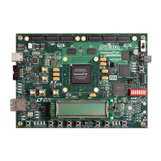
Page 9: Introduction
“Statement of China-RoHS Compliance” on page 2–47 ■ Board Overview This section provides an overview of the Cyclone III LS FPGA development board, including an annotated board image and component descriptions. Figure 2–1 provides an overview of the development board features. - Page 10 Push-buttons (D29-D31) (S3 - S6) Switches (S8, S9) Table 2–1 describes the components and lists their corresponding board references. Table 2–1. Cyclone III LS FPGA Development Board Components (Part 1 of 3) Board Reference Type Description Featured Devices FPGA EP3CLS200F780, 780-pin FBGA.
- Page 11 Chapter 2: Board Components 2–3 Board Overview Table 2–1. Cyclone III LS FPGA Development Board Components (Part 2 of 3) Board Reference Type Description Load LED Illuminates when the MAX II CPLD EPM2210 System Controller is actively configuring the FPGA.
-
Page 12: Featured Device: Cyclone Iii Ls Device
2–4 Chapter 2: Board Components Featured Device: Cyclone III LS Device Table 2–1. Cyclone III LS FPGA Development Board Components (Part 3 of 3) Board Reference Type Description S3, S4, S5, S6 User push-button switches Four user push-button switches. Driven low when pressed. -
Page 13: I/O Resources
49 I/O 59 I/O 58 I/O Table 2–4 lists the Cyclone III LS device pin count and usage by function on the development board. Table 2–4. Cyclone III LS Device Pin Count and Usage (Part 1 of 2) Function I/O Standard... -
Page 14: Max Ii Cpld Epm2210 System Controller
2–6 Chapter 2: Board Components MAX II CPLD EPM2210 System Controller Table 2–4. Cyclone III LS Device Pin Count and Usage (Part 2 of 2) Function I/O Standard I/O Count Special Pins LEDs 1.8-V CMOS 1 INIT_DONE Clocks or Oscillators 1.8-V / 2.5-V CMOS + LVDS... - Page 15 Anti-Tamper example design JTAG connector FPGA_TDO — Anti-Tamper example design JTAG connector FPGA_TMS FSM bus address FSM_A0 AD14 FSM bus address FSM_A1 AA17 FSM bus address FSM_A2 © October 2009 Altera Corporation Cyclone III LS FPGA Development Board Reference Manual...
- Page 16 FSM bus data FSM_D10 AF20 FSM bus data FSM_D11 AH25 FSM bus data FSM_D12 AE18 FSM bus data FSM_D13 FSM bus data FSM_D14 AG20 FSM bus data FSM_D15 Cyclone III LS FPGA Development Board Reference Manual © October 2009 Altera Corporation...
- Page 17 FPGA configuration done LED MAX_CONF_DONE — DIP - Anti-Tamper example design MAX_DIP0 — DIP - Anti-Tamper example design MAX_DIP1 — DIP - Anti-Tamper example design ON/OFF AT_ACTIVE © October 2009 Altera Corporation Cyclone III LS FPGA Development Board Reference Manual...
- Page 18 Table 2–6. MAX II CPLD EPM2210 System Controller Component Reference and Manufacturing Information Manufacturing Manufacturer Board Reference Description Manufacturer Part Number Website IC - MAX II CPLD EPM2210 Altera Corporation EPM2210F256C3N www.altera.com 256FBGA -3 LF 2.5 V VCCINT Cyclone III LS FPGA Development Board Reference Manual © October 2009 Altera Corporation...
-
Page 19: Configuration, Status, And Setup Elements
The USB-Blaster is implemented using a USB Type-B connector (J4), a FTDI USB 2.0 PHY device (U11), and an Altera MAX IIZ CPLD (U13). This allows the configuration of the FPGA using a USB cable directly connected between the USB port on the board (J4) and a USB port of a PC running the Quartus II software. - Page 20 When a shunt is installed on the JTAG_AT_SEL jumper (J12), the default JTAG chain breaks and the MAX II EPM2210 System Controller gains control of the FPGA JTAG. For more information on the anti-tamper example design, refer to <install_dir>\kits\cycloneIIILS_3cls200_fpga\examples\max2\at_example\ readme_at_example.txt. Cyclone III LS FPGA Development Board Reference Manual © October 2009 Altera Corporation...
-
Page 21: Fpga Programming From Flash Memory
The PFL megafunction is a block of logic that is programmed into an Altera programmable logic device (FPGA or CPLD). The PFL functions as a utility for writing to a compatible flash memory device. This... - Page 22 FLASH_WEn FLASH_RYBSYn PGM_LED0 FLASH_CLK FLASH_RSTn PGM_LED1 FLASH_ADVn PGM_LED2 2.5 V Flash FLASH_A [25:1] 10 k FLASH_D [15:0] FLASH_CEn FLASH_OEn FLASH_WEn FLASH_RYBSYn FLASH_CLK FLASH_RESETn FLASH_WPn FLASH_ADVn 10 k Cyclone III LS FPGA Development Board Reference Manual © October 2009 Altera Corporation...
- Page 23 (S8) loads the FPGA with a hardware page based on which PGM_LED[2:0] (D29, D30, D31) LED is illuminated. Table 2–8 defines the hardware page that loads when the PGM configure push-button switch (S8) is pressed. © October 2009 Altera Corporation Cyclone III LS FPGA Development Board Reference Manual...
-
Page 24: Fpga Programming Over External Usb-Blaster
FPGA. Driven by the MAX II CPLD EPM2210 System Controller. FACTORY Green LED. Illuminates when the factory image is loaded to the FPGA. Driven by the MAX II CPLD EPM2210 System Controller. Cyclone III LS FPGA Development Board Reference Manual © October 2009 Altera Corporation... -
Page 25: Setup Elements
The board settings DIP switch (SW2) controls various features specific to the board and the MAX II CPLD EPM2210 System Controller logic design. Table 2–11 shows the switch controls and descriptions. © October 2009 Altera Corporation Cyclone III LS FPGA Development Board Reference Manual... -
Page 26: Jtag Chain Header Switch
JTAG Chain Header Switch The JTAG chain header switch (J11) is provided to either remove or include devices in the active JTAG chain. However, the Cyclone III LS FPGA device is always in the JTAG chain. Refer to Figure 2–4 on page 2–12 for the JTAG chain functionality. -
Page 27: Anti-Tamper Jtag Select Header Switch
The LCD/HSMC port B data select header switch (J18) is provided to control data multiplexing of the LCD and HSMB_D[65:75]signals to the Cyclone III LS device. If the shunt is not placed on the jumper, the FPGA can control the LCD_HSMB_SEL signal. -
Page 28: Configuration Push-Button Switches
This section describes the board's clock inputs and outputs. Cyclone III LS FPGA Clock Inputs Figure 2–6 shows the Cyclone III LS FPGA development board clock inputs. Cyclone III LS FPGA Development Board Reference Manual © October 2009 Altera Corporation... - Page 29 25 MHz Crystal Table 2–20 shows the external clock inputs for the Cyclone III LS FPGA development board. Table 2–20. Cyclone III LS FPGA Development Board Clock Inputs (Part 1 of 2) Schematic Signal Cyclone III LS Source Name Device Pin Number...
-
Page 30: Cyclone Iii Ls Fpga Clock Outputs
2–22 Chapter 2: Board Components Clock Circuitry Table 2–20. Cyclone III LS FPGA Development Board Clock Inputs (Part 2 of 2) Schematic Signal Cyclone III LS Source Name Device Pin Number Standard Description Samtec HSMC AG16 LVTTL inputs from the installed HSMC port A... -
Page 31: General User Input/Output
Board references S3 through S6 are push-button switches that allow you to interact with the Cyclone III LS device. When the switch is pressed and held down, the device pin is set to logic 0; when the switch is released, the device pin is set to logic 1. There is no board-specific function for these general user push-button switches. -
Page 32: User-Defined Dip Switches
Table 2–26. User-Defined DIP Switch Component Reference and Manufacturing Information Manufacturer Board Reference Description Manufacturer Part Number Manufacturer Website Four-position DIP switch C & K Components TDA04H0SB1 www.ck-components.com Cyclone III LS FPGA Development Board Reference Manual © October 2009 Altera Corporation... -
Page 33: User-Defined Leds
LCD signals and the HSMB_D[65:75] signals to the Cyclone III LS device. If the shunt is not placed on the jumper, the FPGA can control the LCD_HSMB_SEL signal. When the LCD_HSMB_SEL signal is set to '1' (shunt removed), the FPGA controls the HSMB_D[65:75] signals. - Page 34 Table 2–30. LCD Pin Definitions and Functions (Part 1 of 2) Number Symbol Level Function — Power supply — GND (0 V) — For LCD drive Register select signal H: Data input L: Instruction input Cyclone III LS FPGA Development Board Reference Manual © October 2009 Altera Corporation...
-
Page 35: Components And Interfaces
2×16 character display, 5×8 dot matrix Lumex Inc. LCM-S01602DSR/C www.lumex.com Components and Interfaces This section describes the development board's communication ports and interface cards relative to the Cyclone III LS device. The development board supports the following communication ports: 10/100/1000 Ethernet ■ HSMC ■... - Page 36 Table 2–33. Ethernet PHY Component Reference and Manufacturing Information Board Manufacturing Manufacturer Reference Description Manufacturer Part Number Website Ethernet PHY BASE-T device Marvell Semiconductor 88E1111-B2-CAAIC000 www.marvell.com Cyclone III LS FPGA Development Board Reference Manual © October 2009 Altera Corporation...
-
Page 37: High-Speed Mezzanine Cards
HSMC port B interface only supports single-ended signaling. The HSMC interface also allows JTAG, SMB, clock outputs and inputs, as well as power for compatible HSMC cards. The HSMC is an Altera-developed open specification, which allows you to expand the functionality of the development board through the addition of daughtercards (HSMCs). - Page 38 LVDS RX bit 5 or CMOS bit 25 HSMA_RX_P5 J2.79 LVDS TX bit 5n or CMOS bit 26 HSMA_TX_N5 J2.80 LVDS RX bit 5n or CMOS bit 27 HSMA_RX_N5 Cyclone III LS FPGA Development Board Reference Manual © October 2009 Altera Corporation...
- Page 39 LVDS RX bit 13n or CMOS bit 63 HSMA_RX_N13 J2.137 LVDS TX bit 14 or CMOS bit 64 AF28 HSMA_TX_P14 J2.138 LVDS RX bit 14 or CMOS bit 65 HSMA_RX_P14 © October 2009 Altera Corporation Cyclone III LS FPGA Development Board Reference Manual...
- Page 40 J1.40 Dedicated CMOS clock in HSMB_CLKIN0 J1.41 Dedicated CMOS I/O bit 0 HSMB_D0 J1.42 Dedicated CMOS I/O bit 1 HSMB_D1 J1.43 Dedicated CMOS I/O bit 2 HSMB_D2 Cyclone III LS FPGA Development Board Reference Manual © October 2009 Altera Corporation...
- Page 41 Dedicated CMOS I/O bit 37 HSMB_D37 J1.97 Dedicated CMOS I/O bit 38 HSMB_D38 J1.98 Dedicated CMOS I/O bit 39 HSMB_D39 J1.101 Dedicated CMOS I/O bit 40 HSMB_D40 © October 2009 Altera Corporation Cyclone III LS FPGA Development Board Reference Manual...
- Page 42 Dedicated CMOS I/O bit 71 when LCD_HSMB_D71 LCD_HSMB_SEL is set to a logic 1. U27.4 Dedicated CMOS I/O bit 72 when LCD_HSMB_D72 LCD_HSMB_SEL is set to a logic 1. Cyclone III LS FPGA Development Board Reference Manual © October 2009 Altera Corporation...
-
Page 43: Memory
ASP-122953-01 www.samtec.com family high-speed socket. Memory This section describes the board's memory interface support and also their signal names, types, and connectivity relative to the Cyclone III LS device. The board has the following memory interfaces: ■ DDR2 ■ SSRAM ■... -
Page 44: Ddr2
Table 2–37 lists the DDR2 bank 7 pin assignments, signal names, and its functions. The signal names and types are relative to the Cyclone III LS device in terms of I/O setting and direction. Table 2–37. DDR2 Bank 7 Pin Assignments, Signal Names and Functions (Part 1 of 2) - Page 45 Table 2–38 lists the DDR2 bank 8 pin assignments, signal names, and its functions. The signal names and types are relative to the Cyclone III LS device in terms of I/O setting and direction. Table 2–38. DDR2 Bank 8 Pin Assignments, Signal Names and Functions (Part 1 of 2)
- Page 46 Data bus byte lane 3 DDR2_DQ30 U5.B9 Data bus byte lane 3 DDR2_DQ31 U5.F7 Data strobe P byte lane 2 DDR2_DQS2 U5.B7 Data strobe P byte lane 3 DDR2_DQS3 Cyclone III LS FPGA Development Board Reference Manual © October 2009 Altera Corporation...
-
Page 47: Ssram
Table 2–40 lists the SSRAM pin assignments, signal names, and functions. The signal names and types are relative to the Cyclone III LS device in terms of I/O setting and direction. Table 2–40. SSRAM Pin Assignments, Schematic Signal Names, and Functions (Part 1 of 3) - Page 48 FSM_D29 U14.M1 Data bus FSM_D30 U14.M2 Data bus AD16 FSM_D31 U14.A8 Address status controller AH19 SRAM_ADSCn U14.B9 Address status processor AB18 SRAM_ADSPn U14.A9 Address valid AB20 SRAM_ADVn Cyclone III LS FPGA Development Board Reference Manual © October 2009 Altera Corporation...
-
Page 49: Flash
440 µs for a 32-word buffer. The erase time is 400 ms for a 32 K parameter block and 1200 ms for a 128 K main block. © October 2009 Altera Corporation Cyclone III LS FPGA Development Board Reference Manual... - Page 50 Table 2–42 lists the flash pin assignments, signal names, and functions. The signal names and types are relative to the Cyclone III LS device in terms of I/O setting and direction. Table 2–42. Flash Pin Assignments, Schematic Signal Names, and Functions (Part 1 of 2)
-
Page 51: Eeprom
Table 2–44 lists the EEPROM pin assignments, signal names, and functions. The signal names and types are relative to the Cyclone III LS device in terms of I/O setting and direction. Table 2–44. EEPROM Pin Assignments, Schematic Signal Names, and Functions... -
Page 52: Power Supply
Figure 2–10 shows the power distribution system on the development board. Regulator inefficiencies and sharing are reflected in the currents shown, which are conservative absolute maximum levels. Cyclone III LS FPGA Development Board Reference Manual © October 2009 Altera Corporation... -
Page 53: Power Measurement
ADC to measure voltage and current. A SPI bus connects these ADC devices to the MAX II CPLD EPM2210 System Controller as well as the Cyclone III LS FPGA. © October 2009 Altera Corporation... - Page 54 Table 2–47. Power Measurement ADC Component Reference and Manufacturing Information Manufacturing Manufacturer Board Reference Description Manufacturer Part Number Website 8-channel differential 24-bit ADC Linear Technology LTC2418CGN#PBF www.linear.com Cyclone III LS FPGA Development Board Reference Manual © October 2009 Altera Corporation...
-
Page 55: Statement Of China-Rohs Compliance
(2) X* indicates that the concentration of the hazardous substance of at least one of all homogeneous materials in the parts is above the relevant threshold of the SJ/T11363-2006 standard, but it is exempted by EU RoHS. © October 2009 Altera Corporation Cyclone III LS FPGA Development Board Reference Manual... - Page 56 2–48 Chapter 2: Board Components Statement of China-RoHS Compliance Cyclone III LS FPGA Development Board Reference Manual © October 2009 Altera Corporation...
-
Page 57: Revision History
Non-technical support (General) Email nacomp@altera.com (Software Licensing) Email authorization@altera.com Note to Table: (1) You can also contact your local Altera sales office or sales representative. © October 2009 Altera Corporation Cyclone III LS FPGA Development Board Reference Manual Preliminary... -
Page 58: Typographic Conventions
A warning calls attention to a condition or possible situation that can cause you injury. The angled arrow instructs you to press Enter. The feet direct you to more information about a particular topic. Cyclone III LS FPGA Development Board Reference Manual © October 2009 Altera Corporation Preliminary...
Need help?
Do you have a question about the Cyclone III LS and is the answer not in the manual?
Questions and answers