
Subscribe to Our Youtube Channel
Related Manuals for Altera Cyclone IV GX FPGA


Summary of Contents for Altera Cyclone IV GX FPGA
- Page 1 Cyclone IV GX FPGA Development Board Reference Manual 101 Innovation Drive San Jose, CA 95134 www.altera.com MNL-01058-1.2 Feedback Subscribe...
- Page 2 © 2015 Altera Corporation. All rights reserved. ALTERA, ARRIA, CYCLONE, HARDCOPY, MAX, MEGACORE, NIOS, QUARTUS and STRATIX words and logos are trademarks of Altera Corporation and registered in the U.S. Patent and Trademark Office and in other countries. All other words and logos identified as trademarks or service marks are the property of their respective holders as described at www.altera.com/common/legal.html.
-
Page 3: Table Of Contents
Statement of China-RoHS Compliance ........... . 2–50 August 2015 Altera Corporation Cyclone IV GX FPGA Development Board Reference Manual... - Page 4 How to Contact Altera ........
-
Page 5: Chapter 1. Overview
Nios II embedded soft processor. The board provides peripherals and memory interfaces to facilitate the development of the Cyclone IV GX FPGA designs. For more information on the Cyclone IV device family, refer to the Cyclone IV Device Handbook. - Page 6 DIP switches ■ Board settings DIP switch ■ JTAG chain select DIP switch ■ PCIe control DIP switch ■ Configuration settings DIP switch ■ User DIP switch ■ Cyclone IV GX FPGA Development Board August 2015 Altera Corporation Reference Manual...
-
Page 7: Development Board Block Diagram
PCIe small form factor board ■ Bench-top operation ■ Development Board Block Diagram Figure 1–1 shows the block diagram of the Cyclone IV GX FPGA development board. Figure 1–1. Cyclone IV GX FPGA Development Board Block Diagram 32 MB DDR2 RJ45 Power (x32) -
Page 8: Handling The Board
When handling the board, it is important to observe the following static discharge precaution: Without proper anti-static handling, the board can be damaged. Therefore, use anti-static handling precautions when touching the board. Cyclone IV GX FPGA Development Board August 2015 Altera Corporation Reference Manual... -
Page 9: Introduction
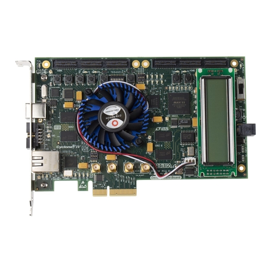
2. Board Components Introduction This chapter introduces the major components on the Cyclone IV GX FPGA development board. Figure 2–1 illustrates major component locations and Table 2–1 provides a brief description of all component features of the board. A complete set of schematics, a physical layout database, and GERBER files for the development board reside in the Cyclone IV GX FPGA development kit documents directory. -
Page 10: Board Overview
2–2 Chapter 2: Board Components Board Overview Board Overview This section provides an overview of the Cyclone IV GX FPGA development board, including an annotated board image and component descriptions. Figure 2–1 provides an overview of the development board features. - Page 11 Chapter 2: Board Components 2–3 Board Overview Table 2–1. Cyclone IV GX FPGA Development Board Components (Part 2 of 3) Board Reference Type Description Illuminates when the MAX II CPLD EPM2210 System Controller is Load LED actively configuring the FPGA.
- Page 12 2–4 Chapter 2: Board Components Board Overview Table 2–1. Cyclone IV GX FPGA Development Board Components (Part 3 of 3) Board Reference Type Description General User Input/Output D7–D10, User LEDs Eight user LEDs. Illuminates when driven low. D12–D15 S1–S4 User push buttons Four user push buttons.
-
Page 13: Featured Device: Cyclone Iv Gx Device
Featured Device: Cyclone IV GX Device Featured Device: Cyclone IV GX Device The Cyclone IV GX FPGA development board features the Cyclone IV GX EP4CGX150DF31 device (U10) in a 896-pin FBGA package. For more information about Cyclone IV device family, refer to the Cyclone IV Device Handbook. -
Page 14: I/O Resources
(10) The dedicated clock input I/O banks 3A, 3B, 8A, and 8B can be used either for HSSI input reference clock pins or clock input pins. (11) Single-ended clock input support is available for dedicated clock input I/O banks 3B and 8B. Cyclone IV GX FPGA Development Board August 2015 Altera Corporation... -
Page 15: Max Ii Cpld Epm2210 System Controller
2–4: (1) Translated from 1.8-V to 2.5-V using a bidirectional voltage translator. MAX II CPLD EPM2210 System Controller The board utilizes the EPM2210 System Controller, an Altera MAX II CPLD, for the following purposes: ■ FPGA configuration from flash memory ■... - Page 16 125-MHz programming data CLKA_SDA — 125-MHz programming clock CLKA_SCL 2.5-V — 125-MHz oscillator enable CLK125_EN — 50-MHz oscillator CLKIN_50 — MAX II clock input CLKIN_MAX_100 — Fan control FAN_CNTL Cyclone IV GX FPGA Development Board August 2015 Altera Corporation Reference Manual...
- Page 17 FPGA configuration done FPGA_CONF_DONE FPGA configuration ready FPGA_STATUSn FPGA configuration active FPGA_CONFIGn FPGA JTAG TCK JTAG_TCK FPGA JTAG TMS JTAG_TMS FPGA JTAG TDO JTAG_FPGA_TDO MAX II JTAG TDO JTAG_EPM2210_TDO August 2015 Altera Corporation Cyclone IV GX FPGA Development Board Reference Manual...
- Page 18 FSM_A17 FSM bus address FSM_A18 FSM bus address FSM_A19 FSM bus address FSM_A20 AK25 FSM bus address FSM_A21 AE21 FSM bus address FSM_A22 AA18 FSM bus address FSM_A23 Cyclone IV GX FPGA Development Board August 2015 Altera Corporation Reference Manual...
- Page 19 — Power monitor SPI data in SENSE_SDI — Power monitor SPI data out SENSE_SDO 1.8-V AF27 System reset push button SYS_RESETn 2.5-V — User reset push button USER_FACTORY August 2015 Altera Corporation Cyclone IV GX FPGA Development Board Reference Manual...
-
Page 20: Configuration, Status, And Setup Elements
The USB-Blaster is implemented using a USB Type-B connector (J4), a FTDI USB 2.0 PHY device (U4), and an Altera MAX II CPLD (U7). This allows the configuration of the FPGA using a USB cable directly connected between the USB port on the board (J4) and a USB port of a PC running the Quartus II software. - Page 21 PCIE_JTAG_EN SW5.4 The Cyclone IV GX FPGA is configured via JTAG using the MAX II configuration controller design (embedded blaster) as the primary configuration mode. The board includes a MAX II CPLD EPM2210 System Controller which interfaces directly to the Cyclone IV GX FPGA for configuration, LCD control, power monitor control, and other purposes.
-
Page 22: Fpga Configuration From Flash Memory
The PFL megafunction is a block of logic that is programmed into an Altera programmable logic device (FPGA or CPLD). The PFL functions as a utility for writing to a compatible flash memory device. This... -
Page 23: Fpga Configuration Using External Usb-Blaster
EPCS device is to use the Serial FlashLoader (SFL), a JTAG-based in-system programming solution for Altera serial configuration devices. The SFL is a bridge design for the FPGA that uses the JTAG connector (J6) to access the JTAG Indirect Configuration Device Programming File (.jic) and then uses the AS interface to... -
Page 24: Status Elements
Green LED. Illuminates to indicate Ethernet PHY transmit activity. Driven ENET TX by the Marvell 88E1111 PHY. Green LED. Illuminates to indicate Ethernet PHY receive activity. Driven ENET RX by the Marvell 88E1111 PHY. Cyclone IV GX FPGA Development Board August 2015 Altera Corporation Reference Manual... -
Page 25: Setup Elements
ON : 100-MHz oscillator input select SW1.4 CLKA_SEL OFF : SMA input select Note to Table 2–10: (1) ON indicates a setting of ’0’ while OFF indicates a setting of ’1’. August 2015 Altera Corporation Cyclone IV GX FPGA Development Board Reference Manual... -
Page 26: Jtag Chain Select Dip Switch
Table 2–13. JTAG Chain Select DIP Switch Component Reference and Manufacturing Information Board Manufacturer Description Manufacturer Manufacturer Website Reference Part Number Four-position slide DIP switch C & K Components TDA04H0SB1 www.ck-components.com Cyclone IV GX FPGA Development Board August 2015 Altera Corporation Reference Manual... -
Page 27: Pcie Control Dip Switch
(1) ON indicates a setting of ’0’ while OFF indicates a setting of ’1’. (2) X indicates does not care. The JTAG-based configuration takes precedence over other configuration schemes and therefore, the MSEL[] pin settings are ignored. August 2015 Altera Corporation Cyclone IV GX FPGA Development Board Reference Manual... -
Page 28: Configuration Push Buttons
The PCIe reference clock is on bank 3A while the 125-MHz clock is on bank Figure 2–5 shows the Cyclone IV GX FPGA development board’s transceiver clock structure. Figure 2–5. Cyclone IV GX FPGA Development Board Transceiver Clock Structure LVPECL Input Clock (J11, J12) FPGA CLKOUT SMA (J9) -
Page 29: General User Input/Output
Table 2–19. User-Defined Push Button Component Reference and Manufacturing Information Manufacturer Board Reference Description Manufacturer Manufacturer Website Part Number S1–S6 Push button Panasonic EVQPAC07K www.panasonic.com/industrial/ August 2015 Altera Corporation Cyclone IV GX FPGA Development Board Reference Manual... -
Page 30: User-Defined Leds
HSMC LEDs. However, the LEDs are labeled TX and RX, and are intended to display data flow to and from the connected HSMC cards. The LEDs are driven by the Cyclone IV GX device. Cyclone IV GX FPGA Development Board August 2015 Altera Corporation Reference Manual... -
Page 31: User-Defined Dip Switch
OPEN or OFF position, a logic 1 is USER_DIPSW3 2.5-V SW2.5 selected. When the switch is in the USER_DIPSW4 SW2.6 CLOSED or ON position, a logic 0 is USER_DIPSW5 SW2.7 selected. USER_DIPSW6 SW2.8 USER_DIPSW7 August 2015 Altera Corporation Cyclone IV GX FPGA Development Board Reference Manual... -
Page 32: Lcd
2–26: (1) All signals are translated from 1.8-V to 2.5-V using a dual/quad low-voltage level translators except for LCD_DATA4, which connects directly to the PLL4_CLKOUTn pin of the Cyclone IV GX FPGA. Cyclone IV GX FPGA Development Board August 2015 Altera Corporation... - Page 33 Board Manufacturer Manufacturer Description Manufacturer Reference Part Number Website 2×7 pin, 100 mil, vertical header Samtec TSM-107-07-G-D www.samtec.com 2×16 character display, 5×8 dot matrix Lumex Inc. LCM-S01602DSR/C www.lumex.com August 2015 Altera Corporation Cyclone IV GX FPGA Development Board Reference Manual...
-
Page 34: Components And Transceiver Interfaces
HSMC PCIe The Cyclone IV GX FPGA development board fits entirely into a PC motherboard with a ×4 PCIe slot which can accommodate a short-form PCIe add-in card. The development board comes with a full height I/O bracket for its low profile form factor card. - Page 35 (1) This signal is multiplexed with the signal on HSMC port B interface. (2) The Quartus II version 10.1sp1 and newer only support an I/O standard of 1.5-V PCML for the PCI Express transmitter as stated in Altera’s knowledge base webpage—solution ID rd12272010_575.
-
Page 36: 10/100/1000 Ethernet
The MAC function must be provided in the FPGA for typical networking applications such the Altera Triple Speed Ethernet MegaCore design. The Marvell 88E1111 PHY uses 2.5-V and 1.1-V power rails and requires a 25-MHz reference clock driven from a dedicated oscillator. -
Page 37: Transceiver Connector (Optional)
PCIe or the HSMC port B interface. The default stuffing option is the PCIe interface. August 2015 Altera Corporation Cyclone IV GX FPGA Development Board Reference Manual... -
Page 38: High-Speed Mezzanine Cards
HSMC port B interface only supports single-ended signaling. The HSMC interface also allows JTAG, SMB, clock outputs and inputs, as well as power for compatible HSMC cards. The HSMC is an Altera-developed open specification, which allows you to expand the functionality of the development board through the addition of daughtercards. - Page 39 Dedicated CMOS I/O bit 0 2.5-V AC27 HSMA_D0 J1.42 Dedicated CMOS I/O bit 1 HSMA_D1 J1.43 Dedicated CMOS I/O bit 2 AF30 HSMA_D2 J1.44 Dedicated CMOS I/O bit 3 AD27 HSMA_D3 August 2015 Altera Corporation Cyclone IV GX FPGA Development Board Reference Manual...
- Page 40 LVDS TX bit 7 or CMOS bit 32 HSMA_TX_D_P7 J1.90 LVDS RX bit 7 or CMOS bit 33 HSMA_RX_D_P7 J1.91 LVDS TX bit 7n or CMOS bit 34 HSMA_TX_D_N7 Cyclone IV GX FPGA Development Board August 2015 Altera Corporation Reference Manual...
- Page 41 LVDS TX bit 15n or CMOS bit 70 HSMA_TX_D_N15 J1.146 LVDS RX bit 15n or CMOS bit 71 HSMA_RX_D_N15 J1.149 LVDS TX bit 16 or CMOS bit 72 HSMA_TX_D_P16 August 2015 Altera Corporation Cyclone IV GX FPGA Development Board Reference Manual...
- Page 42 Management serial data — U39.1 HSMB_T_SDA J2.34 Management serial clock — U39.8 HSMB_T_SCL 2.5-V J2.37 JTAG data output — U2.5 HSMB_JTAG_TDO J2.38 JTAG data input — U1.9; U2.2 HSMB_JTAG_TDI Cyclone IV GX FPGA Development Board August 2015 Altera Corporation Reference Manual...
- Page 43 J2.89 CMOS bit 32 — U36.14 HSMB_T_TX_D_P7 J2.90 CMOS bit 33 — U38.15 HSMB_T_RX_D_P7 J2.91 CMOS bit 34 — U36.15 HSMB_T_TX_D_N7 J2.92 CMOS bit 35 — U38.12 HSMB_T_RX_D_N7 August 2015 Altera Corporation Cyclone IV GX FPGA Development Board Reference Manual...
- Page 44 J2.145 CMOS bit 70 — U28.19 HSMB_T_TX_D_N15 J2.146 CMOS bit 71 — U28.17 HSMB_T_RX_D_N15 J2.149 CMOS bit 72 — U35.12 HSMB_T_TX_D_P16 J2.150 CMOS bit 73 — U28.18 HSMB_T_RX_D_P16 Cyclone IV GX FPGA Development Board August 2015 Altera Corporation Reference Manual...
- Page 45 U37.8 HSMB_RX_D_P12 — — AG16 U29.9 HSMB_RX_D_P13 — — U28.6 HSMB_RX_D_P14 — — AK13 U28.5 HSMB_RX_D_P15 — Management serial data U39.5 HSMB_SCL — Management serial clock U39.4 HSMB_SDA August 2015 Altera Corporation Cyclone IV GX FPGA Development Board Reference Manual...
- Page 46 HSMC Port B Transceiver Cyclone IV GX Device Pin PCIe Signal Signal Number HSMB_RX_N0 XCVR_RX_N0 HSMB_RX_N1 XCVR_RX_N1 HSMB_RX_N2 XCVR_RX_N2 HSMB_RX_N3 XCVR_RX_N3 HSMB_RX_P0 XCVR_RX_P0 HSMB_RX_P1 XCVR_RX_P1 HSMB_RX_P2 XCVR_RX_P2 HSMB_RX_P3 XCVR_RX_P3 HSMB_TX_N0 XCVR_TX_N0 Cyclone IV GX FPGA Development Board August 2015 Altera Corporation Reference Manual...
-
Page 47: Memory
10.6 Gbps. The internal bus in the FPGA is typically 2 or 4 times the width at full rate or half rate respectively. For example, a 167 MHz 16-bit interface becomes a 83.5 MHz 64-bit bus. August 2015 Altera Corporation Cyclone IV GX FPGA Development Board Reference Manual... -
Page 48: Ddr2 Sdram Top Port
U8.F1 Data bus byte lane 0 DDR2A_DQ6 U8.F9 Data bus byte lane 0 DDR2A_DQ7 U8.F3 Write mask byte lane 0 DDR2A_DM0 U8.F7 Data strobe byte lane 0 DDR2A_DQS0 Cyclone IV GX FPGA Development Board August 2015 Altera Corporation Reference Manual... - Page 49 U15.B1 Data bus byte lane 3 DDR2A_DQ30 U15.B9 Data bus byte lane 3 DDR2A_DQ31 U15.B3 Write mask byte lane 3 DDR2A_DM3 U15.B7 Data strobe byte lane 3 DDR2A_DQS3 August 2015 Altera Corporation Cyclone IV GX FPGA Development Board Reference Manual...
-
Page 50: Ddr2 Sdram Bottom Port
U19.F1 Data bus byte lane 0 DDR2B_DQ6 U19.F9 Data bus byte lane 0 DDR2B_DQ7 U19.F3 Write mask byte lane 0 DDR2B_DM0 U19.F7 Data strobe byte lane 0 DDR2B_DQS0 Cyclone IV GX FPGA Development Board August 2015 Altera Corporation Reference Manual... - Page 51 Table 2–39. DDR2 Component Reference and Manufacturing Information Manufacturing Manufacturer Board Reference Description Manufacturer Part Number Website 16 M × 16-bit × 4 banks, 533Mbps, U8, U15, U17, U19 Micron MT47H16M16BG-37E:B www.micron.com August 2015 Altera Corporation Cyclone IV GX FPGA Development Board Reference Manual...
-
Page 52: Ssram
U44.59 Data bus FSM_D1 U44.22 Data bus AG21 FSM_D2 U44.63 Data bus FSM_D3 U44.68 Data bus AK28 FSM_D4 U44.72 Data bus AD23 FSM_D5 U44.12 Data bus AG24 FSM_D6 Cyclone IV GX FPGA Development Board August 2015 Altera Corporation Reference Manual... - Page 53 Table 2–41. SSRAM Component Reference and Manufacturing Information Board Manufacturing Description Manufacturer Manufacturer Website Reference Part Number Standard Synchronous Pipelined GS832018GT-200V www.gsitechnology.com SCD, 2 M × 18, 200 MHz August 2015 Altera Corporation Cyclone IV GX FPGA Development Board Reference Manual...
-
Page 54: Flash
Address bus AK23 FSM_A10 U6.D3 Address bus AH17 FSM_A11 U6.C4 Address bus AB21 FSM_A12 U6.A5 Address bus AF19 FSM_A13 U6.B5 Address bus AF12 FSM_A14 U6.C5 Address bus AG27 FSM_A15 Cyclone IV GX FPGA Development Board August 2015 Altera Corporation Reference Manual... -
Page 55: Power Supply
The development board's power is provided through a laptop-style DC power input. The input voltage must be 16 V. The DC voltage is then stepped down to various power rails used by the components on the board. August 2015 Altera Corporation Cyclone IV GX FPGA Development Board Reference Manual... -
Page 56: Power Distribution System
Shunt installed = 2.5 V Shunt not installed = 1.8 V Linear 1.1V Regulator (LTC3026) 1.8V_B3_B4 2.5 V Linear Regulator (LTC3026) 1.8V_B7_B8 VTT_B3_B4 1.8V_B3_B4 TPS51100DGQ VREF_B3_B4 VTT_B7_B8 1.8V_B7_B8 TPS51100DGQ VREF_B7_B8 Cyclone IV GX FPGA Development Board August 2015 Altera Corporation Reference Manual... -
Page 57: Power Measurement
2.5 V and not shunted it is 1.8 V VCCA, PLL analog power VCCA VCC_CLKIN VCCA_GXB, Transceiver buffer power 2.5V_VCCA_VCCH_GXB VCCH_GXB VCCL_GXB PMA auxiliary power 1.2V_VCCL_GXB August 2015 Altera Corporation Cyclone IV GX FPGA Development Board Reference Manual... -
Page 58: Statement Of China-Rohs Compliance
(2) X* indicates that the concentration of the hazardous substance of at least one of all homogeneous materials in the parts is above the relevant threshold of the SJ/T11363-2006 standard, but it is exempted by EU RoHS. Cyclone IV GX FPGA Development Board August 2015 Altera Corporation... - Page 59 Product literature Website www.altera.com/literature Nontechnical support (general) Email nacomp@altera.com (software licensing) Email authorization@altera.com Note to Table: (1) You can also contact your local Altera sales office or sales representative. August 2015 Altera Corporation Cyclone IV GX FPGA Development Board Reference Manual...
- Page 60 Email Subscription Management Center page of the Altera website, where you can sign up to receive update notifications for Altera documents. The feedback icon allows you to submit feedback to Altera about the document. Methods for collecting feedback vary as appropriate for each document.
Need help?
Do you have a question about the Cyclone IV GX FPGA and is the answer not in the manual?
Questions and answers