
Related Manuals for Altera Cyclone II


Summary of Contents for Altera Cyclone II
- Page 1 Cyclone II FPGA Starter Development Board Reference Manual 101 Innovation Drive San Jose, CA 95134 (408) 544-7000 Document Version http://www.altera.com Document Date October 2006...
- Page 2 Altera Corporation in the U.S. and other countries. All other product or service names are the property of their respective holders. Al- tera products are protected under numerous U.S.
-
Page 3: Table Of Contents
Overview ..............................1–1 Hardware Features ........................... 1–2 Software Features ..........................1–2 Block Diagram ............................1–2 Configuring the Cyclone II FPGA ....................... 1–3 JTAG Programming ......................... 1–3 AS Programming ..........................1–4 Configuration Procedure ......................... 1–4 Configuring the FPGA in JTAG Mode ..................1–4 Configuring the EPCS4 Device in AS Mode ................ - Page 4 RS-232 Serial Circuit Pin List ....................2–34 PS/2 Port ............................2–34 PS/2 Circuit Schematic ......................2–34 PS/2 Serial Circuit Pin List ...................... 2–34 VGA Video Port ..........................2–35 Audio Ports ............................. 2–35 SMA External Clock Connector ....................2–36 Power Supply Connector ......................2–36 Altera Corporation Preliminary...
-
Page 5: About This Manual
Table 2–1. Document Revision History Date Description October 2006 Initial publication of the Cyclone II FPGA Starter Development Board Reference Manual, version 1.0. How to Find The following methods enable you to quickly find information in this Portable Document Format (PDF) type document: Information ■... - Page 6 About This Manual For the most up-to-date information about Altera products, go to the Altera world-wide web site at www.altera.com. For technical support on this product, go to www.altera.com/mysupport. For additional information about Altera products, consult the sources shown below.
- Page 7 The warning indicates information that should be read prior to starting or continuing the procedure or processes The angled arrow indicates you should press the Enter key. The feet direct you to more information on a particular topic. Altera Corporation Reference Manual October 2006 Cyclone II FPGA Starter Development Board...
- Page 8 About This Manual viii Reference Manual Altera Corporation Cyclone II FPGA Starter Development Board October 2006...
-
Page 9: Chapter 1. Introduction
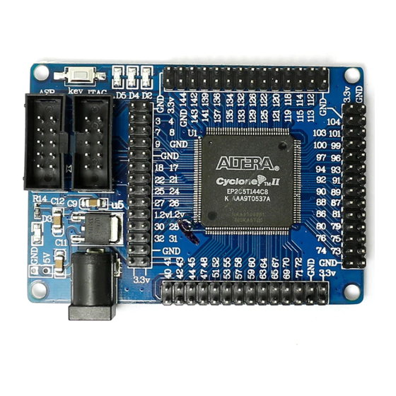
1. Introduction Overview The Cyclone II FPGA Starter Development Board (Figure 1–1) provides integrated features that enable users to develop and test designs that range from simple circuits to various multimedia projects, all without the need to implement complex application programming interfaces (APIs), host control software, or SRAM/SDRAM/flash memory controllers. -
Page 10: Hardware Features
Use of the development board requires familiarity with the Altera Quartus II software. Tutorials for the Quartus II software and for the Cyclone II FPGA Starter Board are available on the Altera web site or on the included development kit CD-ROM in the Examples directory. -
Page 11: Configuring The Cyclone Ii Fpga
Cyclone II FPGA cable, as well as a serial EEPROM chip (EPCS4) that stores configuration data for the Cyclone II FPGA. This configuration data loads automatically from the EEPROM chip into the FPGA each time power is applied to the board. -
Page 12: As Programming
Altera EPCS4 serial EEPROM chip. The EEPROM provides non-volatile storage of the bit stream, retaining the information even when power to the Cyclone II FPGA Starter board is turned off. When the board powers up, the configuration data in the EPCS4 device automatically loads into the Cyclone II FPGA. -
Page 13: Configuring The Epcs4 Device In As Mode
AS configuration setup. To download a configuration bit stream into the EPCS4 serial EEPROM device, perform the following steps: Ensure that power is applied to the Cyclone II FPGA Starter board. Connect the supplied USB cable to the USB-Blaster port on the board. - Page 14 EPCS Serial Configuration Device Component Table 1–1 lists the components, their locations, and brief descriptions. Summary Table 1–1. Cyclone II FPGA Development Board Components & Interfaces (Part 1 of 2) Board Designation Name Description Cyclone II FPGA EP2C20 device User Interface KEY0 –...
-
Page 15: Component Features
Introduction Table 1–1. Cyclone II FPGA Development Board Components & Interfaces (Part 2 of 2) Board Designation Name Description RS232 Serial connector RS-232 9-pin serial connector with 5 V-tolerant buffers. Supports all RS-232 signals. Expansion header connector Expansion header 1 connecting to 40 I/O pins on the... -
Page 16: Serial Configuration Device And Usb Blaster Circuit
Debounced by a Schmitt trigger circuit ■ Normally HIGH; generates one active-LOW pulse when the switch is pressed Toggle Switches ■ 10 toggle switches for user inputs 1–8 Reference Manual Altera Corporation Cyclone II FPGA Starter Development Board October 2006... -
Page 17: Clock Inputs
PS/2 connector for connecting a PS2 mouse or keyboard to the board Dual 40-Pin Expansion Headers ■ 72 Cyclone II I/O pins and 8 power and ground lines connect to two, 40-pin expansion connectors ■ 40-Pin header designed to accept a standard 40-pin ribbon cable used for IDE hard drives ■... - Page 18 Introduction 1–10 Reference Manual Altera Corporation Cyclone II FPGA Starter Development Board October 2006...
-
Page 19: Chapter 2. Development Board Components
SMA external clock connector ● 7.5 V power supply connector ● Cyclone II The main device that defines the starter development board is an Altera ® Cyclone II EP2C20 FPGA in a 484-pin FineLine BGA package. Table 2–1 EP2C20 FPGA lists the FPGA features. -
Page 20: Usb-Blaster Controller
Altera USB-Blaster driver software on a host computer, the USB-Blaster controller enables direct programming of the FPGA. Refer to ((section on Configuring the FPGA)) and the Cyclone II FPGA Starter Development Kit User Guide for further details on configuring the FPGA. -
Page 21: Vga Timing
Table 2–2. VGA Horizontal Timing Specifications Configuration Resolution (HxV) a (μs) b (μs) c (μs) d (μs) Pixel clock (MHz) VGA (60 Hz) 640 x 480 25.4 25 (640/c) Altera Corporation Reference Manual 2–3 October 2006 Cyclone II FPGA Starter Development Board... -
Page 22: Vga Circuit Pin List
VGA Blue[1] VGA_B[2] PIN_A10 VGA Blue[2] VGA_B[3] PIN_B10 VGA Blue[3] VGA_HS PIN_A11 VGA H_SYNC VGA_VS PIN_B11 VGA V_SYNC VGA Circuit Schematic Figure 2–2 shows the VGA circuit schematic. 2–4 Reference Manual Altera Corporation Cyclone II FPGA Starter Development Board October 2006... -
Page 23: Audio Codec
Audio CODEC The development board provides a Wolfson WM8731high-quality, 24-bit, sigma-delta audio encoder/decoder (CODEC) for applications such as MP3 players and recorders, PDAs, smart phones, and voice recorders. Altera Corporation Reference Manual 2–5 October 2006 Cyclone II FPGA Starter Development Board... -
Page 24: Audio Circuit Schematic
BoardDesignFiles\Datasheet folder in the kit installation directory or to the manufacturer's web site. Audio Circuit Schematic Figure 2–3 shows the audio circuit schematic. Figure 2–3. Audio Circuit Schematic Diagram 2–6 Reference Manual Altera Corporation Cyclone II FPGA Starter Development Board October 2006... -
Page 25: Audio Circuit Pin List
For information on the memory devices, refer to the BoardDesignFiles\Datasheet folder in the kit installation directory. SDRAM Schematic and Pin List Figure 2–4 shows the SDRAM interface signals. Altera Corporation Reference Manual 2–7 October 2006 Cyclone II FPGA Starter Development Board... - Page 26 PIN_W4 SDRAM Address[0] DRAM_ADDR[1] PIN_W5 SDRAM Address[1] DRAM_ADDR[2] PIN_Y3 SDRAM Address[2] DRAM_ADDR[3] PIN_Y4 SDRAM Address[3] DRAM_ADDR[4] PIN_R6 SDRAM Address[4] DRAM_ADDR[5] PIN_R5 SDRAM Address[5] DRAM_ADDR[6] PIN_P6 SDRAM Address[6] 2–8 Reference Manual Altera Corporation Cyclone II FPGA Starter Development Board October 2006...
-
Page 27: Sram Schematic And Pin List
SDRAM Clock Enable DRAM_CLK PIN_U4 SDRAM Clock DRAM_WE_N PIN_R8 SDRAM Write Enable DRAM_CS_N PIN_T6 SDRAM Chip Select SRAM Schematic and Pin List Figure 2–5 shows the SRAM interface signals. Altera Corporation Reference Manual 2–9 October 2006 Cyclone II FPGA Starter Development Board... - Page 28 PIN_AB4 SRAM Address[3] SRAM_ADDR[4] PIN_AA5 SRAM Address[4] SRAM_ADDR[5] PIN_AB10 SRAM Address[5] SRAM_ADDR[6] PIN_AA11 SRAM Address[6] SRAM_ADDR[7] PIN_AB11 SRAM Address[7] SRAM_ADDR[8] PIN_V11 SRAM Address[8] SRAM_ADDR[9] PIN_W11 SRAM Address[9] 2–10 Reference Manual Altera Corporation Cyclone II FPGA Starter Development Board October 2006...
-
Page 29: Flash Schematic And Pin List
SRAM High-byte Data Mask SRAM_LB_N PIN_Y7 SRAM Low-byte Data Mask SRAM_CE_N PIN_AB5 SRAM Chip Enable Flash Schematic and Pin List Figure 2–6 shows the Flash memory interface signals. Altera Corporation Reference Manual 2–11 October 2006 Cyclone II FPGA Starter Development Board... - Page 30 PIN_R14 FLASH Address[8] FL_ADDR[9] PIN_Y13 FLASH Address[9] FL_ADDR[10] PIN_R12 FLASH Address[10] FL_ADDR[11] PIN_T12 FLASH Address[11] FL_ADDR[12] PIN_AB14 FLASH Address[12] FL_ADDR[13] PIN_AA13 FLASH Address[13] FL_ADDR[14] PIN_AB13 FLASH Address[14] 2–12 Reference Manual Altera Corporation Cyclone II FPGA Starter Development Board October 2006...
-
Page 31: Clock Circuit
■ Input through the USB-Blaster port can provide a 24 MHz clock. Clock Circuit Schematic Figure 2–7 shows the clock circuit schematic. Altera Corporation Reference Manual 2–13 October 2006 Cyclone II FPGA Starter Development Board... -
Page 32: Clock Input Pin List
External (SMA) clock input Switches The development board provides the following user switches: ■ Power ON/OFF switch ■ RUN/PROG switch ■ 4 push button switches ■ 10 Toggle switches 2–14 Reference Manual Altera Corporation Cyclone II FPGA Starter Development Board October 2006... -
Page 33: Power On/Off Switch
Development Board Components Power ON/OFF Switch The Cyclone II FPGA Starter board receives its power from either the USB port directly or the included 7.5V power adapter. The Power On/Off switch gates the power from both of these sources to the rest of the board. -
Page 34: Push Button Switches
HIGH logic level at 3.3 volts when released. A Schmitt Trigger circuit on each switch debounces the signal (Figure 2–11). Figure 2–11. Switch Debouncing 2–16 Reference Manual Altera Corporation Cyclone II FPGA Starter Development Board October 2006... -
Page 35: Push Button Switch Schematic
SW0–SW9, located at the bottom left on the development board below the red LEDs, LEDR0-LEDR9 (Figure 2–13). Not debounced, these switches provide level-sensitive data inputs to a circuit. Each switch Altera Corporation Reference Manual 2–17 October 2006 Cyclone II FPGA Starter Development Board... -
Page 36: Toggle Switch Schematic
Figure 2–13. Toggle Switches SW0–SW9 and Red LEDs LEDR0-LEDR9 Toggle Switch Schematic Figure 2–14 shows a schematic diagram of the toggle switches. Figure 2–14. Toggle Switch Schematic Diagram 2–18 Reference Manual Altera Corporation Cyclone II FPGA Starter Development Board October 2006... -
Page 37: Toggle Switch Pin List
I/O pin. A HIGH logic level on a pin turns the LED on; a LOW logic level on a pin turns the LED off. LED Schematic Figure 2–15 shows a schematic diagram of the LEDs. Altera Corporation Reference Manual 2–19 October 2006 Cyclone II FPGA Starter Development Board... - Page 38 Development Board Components Figure 2–15. LED Schematic Diagram 2–20 Reference Manual Altera Corporation Cyclone II FPGA Starter Development Board October 2006...
-
Page 39: Led Pin List
FPGA. Each segment connects to an FPGA general-purpose I/O pin. A LOW logic level applied at the pin lights up the segment; a HIGH logic level turns the segment off. Altera Corporation Reference Manual 2–21 October 2006 Cyclone II FPGA Starter Development Board... -
Page 40: Seven-Segment Display Schematic
2–17). The development board does not connect or use the dot in the display. Figure 2–17. Segment Index and Position Seven-Segment Display Schematic Figure 2–18 shows a schematic diagram of the LEDs. 2–22 Reference Manual Altera Corporation Cyclone II FPGA Starter Development Board October 2006... -
Page 41: Seven-Segment Display Pin List
Seven-Segment segment 0[3] HEX0[4] PIN_F2 Seven-Segment segment 0[4] HEX0[5] PIN_F1 Seven-Segment segment 0[5] HEX0[6] PIN_E2 Seven-Segment segment 0[6] HEX1[0] PIN_E1 Seven-Segment segment 1[0] HEX1[1] PIN_H6 Seven-Segment segment 1[1] Altera Corporation Reference Manual 2–23 October 2006 Cyclone II FPGA Starter Development Board... -
Page 42: Connectors
SD card connector ■ RS-232 serial port ■ PS/2 port ■ VGA video port ■ Audio microphone-in, line-in, line-out ports ■ SMA external clock connector ■ Power supply connector 2–24 Reference Manual Altera Corporation Cyclone II FPGA Starter Development Board October 2006... -
Page 43: Usb-Blaster Port
Development Board Components USB-Blaster Port The Cyclone II FPGA Starter Board includes USB-Blaster circuitry used for programming the FPGA or the EPCS4 device. A USB type B connector (Figure 2–19) provides the connection to this programming circuitry. Refer to“USB-Blaster Controller” on page 2–2 for more information about the USB Blaster circuitry. -
Page 44: Expansion Header Schematics
Development Board Components Figure 2–20. Expansion Headers Expansion Header Schematics Figure 2–21 shows the JP1 expansion header schematic. 2–26 Reference Manual Altera Corporation Cyclone II FPGA Starter Development Board October 2006... - Page 45 Development Board Components Figure 2–21. Expansion Header JP1 Schematic Diagram Figure 2–22 shows the JP2 expansion header schematic. Altera Corporation Reference Manual 2–27 October 2006 Cyclone II FPGA Starter Development Board...
-
Page 46: Expansion Header Pin List
Table 2–14. Expansion Header FPGA Pin Connections (Part 1 of 3) Signal Name FPGA Pin Description GPIO_0[0] PIN_A13 GPIO Connection 0[0] GPIO_0[1] PIN_B13 GPIO Connection 0[1] GPIO_0[2] PIN_A14 GPIO Connection 0[2] GPIO_0[3] PIN_B14 GPIO Connection 0[3] 2–28 Reference Manual Altera Corporation Cyclone II FPGA Starter Development Board October 2006... - Page 47 GPIO Connection 0[32] GPIO_0[33] PIN_K20 GPIO Connection 0[33] GPIO_0[34] PIN_L19 GPIO Connection 0[34] GPIO_0[35] PIN_L18 GPIO Connection 0[35] GPIO_1[0] PIN_H12 GPIO Connection 1[0] GPIO_1[1] PIN_H13 GPIO Connection 1[1] Altera Corporation Reference Manual 2–29 October 2006 Cyclone II FPGA Starter Development Board...
- Page 48 GPIO Connection 1[30] GPIO_1[31] PIN_N21 GPIO Connection 1[31] GPIO_1[32] PIN_P15 GPIO Connection 1[32] GPIO_1[33] PIN_N15 GPIO Connection 1[33] GPIO_1[34] PIN_P17 GPIO Connection 1[34] GPIO_1[35] PIN_P18 GPIO Connection 1[35] 2–30 Reference Manual Altera Corporation Cyclone II FPGA Starter Development Board October 2006...
-
Page 49: Sd Card Connector
Development Board Components SD Card Connector The Cyclone II FPGA Starter board includes an SD Card connector (U8) (Figure 2–23) to interface with SD Card devices including flash storage. Figure 2–23. SD Card Connector Figure 2–24 shows the schematic diagram of the SD Card interface. -
Page 50: Rs-232 Serial Port
2–25) for RS-232 communications. For detailed information on how to use the transceiver, refer to the BoardDesignFiles\Datasheet folder in the kit installation directory or connect to the manufacturer’s web site. 2–32 Reference Manual Altera Corporation Cyclone II FPGA Starter Development Board October 2006... -
Page 51: Rs-232 Circuit Schematic
Development Board Components Figure 2–25. RS-232 Serial Connector RS-232 Circuit Schematic Figure 2–26 shows the RS-232 serial circuit schematic. Figure 2–26. RS-232 Serial Circuit Schematic Diagram Altera Corporation Reference Manual 2–33 October 2006 Cyclone II FPGA Starter Development Board... -
Page 52: Rs-232 Serial Circuit Pin List
FPGA pins assigned to the PS/2 serial circuit. Table 2–17. PS/2 Serial Circuit FPGA Pin Connections Signal Name FPGA Pin Description PS2_CLK PIN_H15 PS/2 Clock PS2_DAT PIN_J14 PS/2 Data 2–34 Reference Manual Altera Corporation Cyclone II FPGA Starter Development Board October 2006... -
Page 53: Vga Video Port
Development Board Components VGA Video Port The Cyclone II FPGA Starter board includes a video connector (Figure 2–28) that connects to an on-board 4-bit video DAC. The connector is a standard DB15 15-pin analog VGA connector. Refer to “VGA DAC” on page 2–2 for a description of the circuitry attached to this connector. -
Page 54: Sma External Clock Connector
Figure 2–30. SMA Connector for External Clock Input Power Supply Connector The Cyclone II FPGA Starter board receives its power from either the USB port directly or the included 7.5V power adapter, which plugs into power connector J8 (Figure 2–31). - Page 55 Development Board Components Figure 2–31. Power Supply Connector Altera Corporation Reference Manual 2–37 October 2006 Cyclone II FPGA Starter Development Board...
- Page 56 Development Board Components 2–38 Reference Manual Altera Corporation Cyclone II FPGA Starter Development Board October 2006...
Need help?
Do you have a question about the Cyclone II and is the answer not in the manual?
Questions and answers