
Related Manuals for Advantech UTC-320


Summary of Contents for Advantech UTC-320
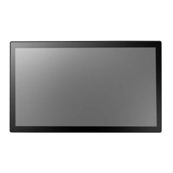
- Page 1 User Manual UTC-320 Ubiquitous Touch Computer with 21.5” TFT LCD and Intel® Processor...
- Page 2 The documentation and the software included with this product are copyrighted 2024 by Advantech Co., Ltd. All rights are reserved. Advantech Co., Ltd. reserves the right to improve the products described in this manual at any time without notice. No part of this manual may be reproduced, copied, translated, or transmitted in any form or by any means without the prior written permission of Advantech Co., Ltd.
-
Page 3: Declaration Of Conformity
Disposal of a BATTERY into fire or a hot oven, or mechanically crushing or cut- ting of a BATTERY, that can result in an explosion. Ensure to connect the power cord to a socket-outlet with earthing connection. UTC-320 User Manual... -
Page 4: Packing List
Packing List Before setting up the product, please ensure that the following items were included: 1 x UTC-320 Accessories for UTC-320, it may varify in case different CPU platforms – 1 x Warranty card – 1 x Power adapter –... -
Page 5: Safety Instructions
In accordance with IEC 704-1:1982, the sound pressure level at the operator's position does not exceed 70 dB (A). DISCLAIMER: These instructions are provided according to IEC 704-1 specifica- tions. Advantech disclaims all responsibility for the accuracy of any statements con- tained herein. UTC-320 User Manual... - Page 6 UTC-320 User Manual...
-
Page 7: Table Of Contents
Touchscreen (Optional) ..............3 1.2.6 Environment.................. 3 LCD Specifications..................4 Optional Modules ..................5 Dimensions ....................6 Figure 1.1 UTC-320 System Dimensions ........6 Chapter System Setup ........7 Quick Tour....................8 Figure 2.1 UTC-320 Front View........... 8 Figure 2.2 UTC-320 Rear View ........... 8 Installation Procedures................ - Page 8 Table A.31:CN11(E): CSAFE ............. 57 Table A.32:CN16(D),CN13(E),CN14(F),CN11(G),CN44(HI): COM2 ............... 57 Table A.33:CN18(D),CN14(E),CN15(F),CN13(GHI): COM1 ..58 Table A.34:CN114(K),CN113(K): COM1,COM2......58 Table A.35:CN21(D),CN16(EF),CN23(G),CN45(H): Power on switch ............... 59 Table A.36:CN45(I): Power on switch......... 59 Table A.37:CN121(K): Power on switch ........59 UTC-320 User Manual viii...
- Page 9 Table A.71:TYPEC2(K): TYPEC USB ........78 Table A.72:TYPEC3(K): TYPEC PD POWER IN......79 Table A.73:CN110(K): GPIO............79 Table A.74:CN13(K): POE LAN IN ..........80 Table A.75:CN119(K): POE PD IN ..........80 Table A.76:BAT1(K): Button battery ........... 80 UTC-320 User Manual...
- Page 10 UTC-320 User Manual...
-
Page 11: Chapter 1 General Information
Chapter General Information This chapter provides general information about UTC-320. Introduction General Specifications LCD Specifications Dimensions... -
Page 12: Introduction
LCD panel. The system can be easily integrated with key periph- erals and display systems for diverse self-service and interactive signage applica- tions. Moreover, with the provision of a removable frame, UTC-320 can also be wall or panel mounted for control applications. -
Page 13: Audio Function
VESA support: 100 x 100 mm (3.93 x 3.93 in) with 10 x M4 screws; supports landscape and portrait modes . Caution! Use suitable mounting apparatus to avoid personal injury. Note! Follow the instructions provided in the user manual to install UTC-320. UTC-320 User Manual... -
Page 14: Lcd Specifications
Luminance: 250 cd/m Note! The UTC-320 color LCD is high quality and reliable. However, it may contain a few defective pixels that do not always illuminate. With current technology, it is impossible to completely eliminate defective pixels. Advantech is actively working to improve this technology. -
Page 15: Optional Modules
1 x 260-pin SODIMM DDR4 3200 MHZ up to 32 GB (UTC-320I) – 1 x 262-pin SO-DIMM DDR5 4800 MHz up to 16 GB (UTC-320K) Operating system: – Windows 10 IoT Enterprise (64 bit) UTC-320 D/F/G/H/I/K – Linux (UTC-320 D/F/G/H/I/K) – Android 6.0 (only UTC-320D) –... -
Page 16: Dimensions
1.5 Dimensions Figure 1.1 UTC-320 System Dimensions UTC-320 User Manual... -
Page 17: Chapter 2 System Setup
Chapter System Setup This chapter explains the initial setup of UTC-320. Quick Tour Installation Procedures BIOS Setup Software Installation Driver Installation... -
Page 18: Quick Tour
Before setting up UTC-320, take a moment to familiarize yourself with the locations and purposes of the controls, drives, connectors, and ports (as shown in the figures below). When UTC-320 is placed upright on a desk top, the front panel should appear as shown in Figure 2.1. Figure 2.1 UTC-320 Front View Located at the rear of UTC-320 is an I/O section that includes serial ports, Ethernet ports, USB ports, HDMI ports, Line-Out/Mic-In, RJ-11, DC-In, and a power button. - Page 19 A. Power button F. HDMI B. USB Type-C DC IN G. 2 x RJ-48 (COM) C. USB Type-C Only H. Line out/ Mic-In D. 2 x LAN I. 2 x USB 2. E. 2 x USB 3.2 UTC-320 User Manual...
-
Page 20: Installation Procedures
Before you start the computer, please connect keyboard port on the I/O section of the UTC-320. 2.2.3 Switching on the Power Supply When you look at the rear side of the UTC-320, you will see the power switch as shown in Figure 2.3. Figure 2.3 Power Cord to DC Input... -
Page 21: Bios Setup
2.3 BIOS Setup The UTC-320 system is likely to have been setup and configured by your dealer prior to delivery. However, users may still find it necessary to use the UTC-320 BIOS setup program to adjust the system configuration data, such as the current date/time or hard drive type. - Page 22 Select “Serial Port 2 Configuration” Configure the Serial Port 2 mode [RS-232/422/485] UTC-320 User Manual...
-
Page 23: Software Installation
If required, insert the OS installation or setup disk into the disk drive until the release button pops out. The UTC-320 BIOS utility supports system boot-up from the CD-ROM drive. The sys- tem installation CD-ROM can be inserted into the CD-ROM drive. - Page 24 UTC-320 User Manual...
-
Page 25: Chapter 3 Hardware Installation And Upgrades
Chapter Hardware Installation and Upgrades This chapter explains how to install the system hardware. Overview HDD Installation mSATA Installation WLAN Installation... -
Page 26: Introduction
3.1 Introduction The UTC-320 is a PC-based computer that is housed in a plastic enclosure. To install an HDD, DRAM, or mini SATA card, simply remove the rear cover. Similarly, any maintenance or hardware upgrades can be easily completed after removing the rear cover. -
Page 27: Msata/M.2 Installation
Remove the 6 screws on the reinforced board. Insert an mSATA/m.2 card into the mSATA/m.2 slot Replace and tighten the screws on the reinforced board. Replace and secure the rear cover. Figure 3.2 Installing an mSATA/m.2 Card UTC-320 User Manual... -
Page 28: Wlan Installation
Two locations are reserved for attaching an external antenna, one is by the I/O port and the other is on the rear cover. Users can choose the antenna location according to their requirements. Remove the 12 screws from the rear cover. Remove the 6 screws on the reinforced board. UTC-320 User Manual... - Page 29 Connect a coaxial cable (Advantech part number: 1750008953-01 for UTC- 320D/E/F, 1750008954-01 for UTC-320G/H/I/K) to ANT1 on the WLAN card. Install the WLAN card on the underside of the motherboard. The wireless antenna cable should be routed as shown below.
- Page 30 UTC-320 User Manual...
-
Page 31: Chapter 4 Jumper And Connector Settings
Chapter Jumper and Connector Settings This chapter provides details for setting jumpers and connecting peripherals, switches, and indica- tors. Jumpers and Connectors Jumper and Connector Functions Jumper and Connector Locations... -
Page 32: Jumpers And Connectors
4.1 Jumpers and Connectors 4.1.1 Jumper Configuration Users can configure UTC-320 according to their application needs by setting jump- ers. A jumper is the simplest type of electrical switch and consists of two metal pins and a small metal clip (typically protected by a plastic cover) that slides over the pins to connect them. -
Page 33: Jumper And Connector Functions
CN25(D),CN20(EF),CN22(G),CN169(HI) External USB CN26(D),CN18(EF),CN20(G),CN43(HI) External USB CN107(K),CN106(K) External USB CN27(D),CN21(E),CN22(F),CN25(G),CN66(HI) Line-out CN28(D),CN22(E),CN21(F),CN24(GHI) MIC-IN CN12(K) MIC-IN&Line-out CN30(D),CN24(EF),CN27(G),CN15(HI)CN16(K) HDMI CN42(H) CN31(DG),CN25(EF),DCIN1(HI) DC-IN CN29(D),CN23(EF),CN26(G) RJ11 CN25(EF),CN31(DG),SW5(HI),CN121(K) Power button CN110(K) GPIO TYPEC3(K) PD POWER IN TYPEC2(K) USB-TYPEC CN13(K),CK119(K) BAT1(K) Button battery UTC-320 User Manual... -
Page 34: Locating Jumpers And Connectors
4.1.3 Locating Jumpers and Connectors PCM-U301(UTC-320D) PCM-U302(UTC-320E) UTC-320 User Manual... - Page 35 PCM-U303(UTC-320F) PCM-U304(UTC-320G) UTC-320 User Manual...
- Page 36 PCM-U305(UTC-320H) PCM-U306(UTC-320I) UTC-320 User Manual...
- Page 37 PCM-8220(UTC-315K/318K/320K) UTC-320 User Manual...
-
Page 38: Jumpers
HD_3x1P_100_D Description PIN HEADER 3x1P 2.54mm 180D(M) DIP 205-1x3GS Setting Function (1-2) (2-3)* 3.3V Table 4.4: JP1(HIK):PWM POWER Part Number 1653003101 Footprint HD_3x1P_79_D Description PIN HEADER 3x1P 2.0mm 180D(M) DIP 2000-13 WS Setting Function (1-2) (2-3)* 3.3V UTC-320 User Manual... - Page 39 Part Number 1653003101 Footprint HD_3x1P_79_D Description PIN HEADER 3x1P 2.0mm 180D(M) DIP 2000-13 WS Setting Function (1-2)* Normal (2-3) CMOS Clear Table 4.8: JP4(HI):TS POWER Part Number 1653002101-02 Footprint HD_2x1P_79_D Description PIN HEADER 2x1P 2.0mm 180D(M) DIP 21N12050 UTC-320 User Manual...
- Page 40 HD_5x2P_79 Description PIN HEADER 5x2P 2.0mm 180D(M) SMD 21N22050 Setting Function (1-3) COM1 RING (2-4) COM2 RING (3-5)* COM1 RI output +5V (4-6)* COM2 RI output +5V (7-9)* COM1 RI output +12V (8-10)* COM2 RI output +12V UTC-320 User Manual...
- Page 41 Setting Function (1-2) (2-3)* Table 4.13: CN10(E): CSAFE Power Part Number 1653003201 Footprint HD_3x2P_79_D Description PIN HEADER 3x2P 2.0mm 180D(M) DIP 21N22050 Setting Function (1-3) * CSAFE output +5V (3-4) CSAFE output +9V (3-5) CSAFE output +12V UTC-320 User Manual...
- Page 42 UTC-320 User Manual...
- Page 43 Appendix I/O Pin Assignments...
-
Page 44: Pin Assignments
1655004512-01 Footprint WF_8P_49_BOX_D Description WAFER BOX 8P 1.25mm 180D(M) DIP A1251WV0-8P Pin name +12V_INVERTER +12V_INVERTER BKLT_EN BRIGHT1 +12V_INVERTER Table A.2: CN2(I):Back Light Part Number 1653008044-01 Footprint WF_8X1P_49_D_H185 Description Wafer 1X8P/1.25/HTN/Sn/VA/D/WH/L2.30mm Pin name +12V_INVERTER +12V_INVERTER BKLT_EN BRIGHT1 +12V_INVERTER UTC-320 User Manual... - Page 45 Table A.3: CN3(D):Internal USB Part Number 1655000453 Footprint WHL5V-2M-24W1140 Description WAFER BOX 2.0mm 5P 180D(M) DIP WO/Pb JIH VEI Pin name Table A.4: CN38(H),CN39(H):Internal USB Part Number 1655305020 Footprint WHL5V-2M Description WAFER BOX 2.0mm 5P 180D(M) DIP A2001WV2-5P Pin name UTC-320 User Manual...
- Page 46 Table A.5: CN38(I),CN39(I):Internal USB Part Number 1653007388-01 Footprint WF_5P_79_BOX_D_H240 Description Wafer 1x5P/2.0mm/NY66+30GF/(M)/VA/Sn/D/WH/H6.1mm Pin name Table A.6: CN115(K),CN118(K),CN116(K),CN104(K),CN103(K) :Internal Part Number 1655000693 Footprint WHL5HS-1M Description WAFER BOX 1x5P 1.0mm 180D(M) SMD 1734595-5 Pin name UTC-320 User Manual...
- Page 47 B/B Conn. 40P 1.25mm 90D SMD DF13-40DP-1.25V(91) Pin name +3.3V or +5V +3.3V or +5V +3.3V or +5V +3.3V or +5V LVDS0_D0- LVDS1_D0- LVDS0_D0+ LVDS1_D0+ GND- LVDS0_D1- LVDS1_D1- LVDS0_D1+ LVDS1_D1+ LVDS0_D2- LVDS1_D2- LVDS0_D2+ LVDS1_D2+- LVDS0_CLK- LVDS1_CLK- LVDS0_CLK+ UTC-320 User Manual...
- Page 48 Table A.7: CN4(DEFG):LVDS LVDS1_CLK+ LVDS0_DDC_SC LVDS0_DDC_SD LVDS0_D3- LVDS1_D3- LVDS0_D3+ LVDS1_D3+ +3.3V or +5V +3.3V or +5V Table A.8: LVDS1(H):LVDS Part Number 1653006918-01 Footprint SPH20X2 Description (DEL20)Wafer 2x20P/1.25mm/(M)/NY9T/VA/GFL/S/WH Pin name +3.3V +3.3V LVDS0_D0- LVDS1_D0- LVDS0_D0+ LVDS1_D0+ GND- LVDS0_D1- UTC-320 User Manual...
- Page 49 Table A.8: LVDS1(H):LVDS LVDS1_D1- LVDS0_D1+ LVDS1_D1+ LVDS0_D2- LVDS1_D2- LVDS0_D2+ LVDS1_D2+- LVDS0_CLK- LVDS1_CLK- LVDS0_CLK+ LVDS1_CLK+ LVDS0_D3- LVDS1_D3- LVDS0_D3+ LVDS1_D3+ UTC-320 User Manual...
- Page 50 Table A.9: LVDS1(I):LVDS Part Number 1655005099-01 Footprint LVDS_40P_50203-04001-001 Description LVDS Conn. 40P 0.5mm 90D(F) SMD 50203-04001-001 Pin name +3.3V +3.3V +3.3V +3.3V LVDS0_D0- LVDS0_D0+ LVDS0_D1- LVDS0_D1+ LVDS0_D2+ LVDS0_D2- LVDS0_CLK- LVDS0_CLK+ LVDS0_D3- LVDS0_D3+ LVDS1_D0- UTC-320 User Manual...
- Page 51 Table A.9: LVDS1(I):LVDS LVDS1_D0+ LVDS1_D1- LVDS1_D1+ LVDS1_D2- LVDS1_D2+ LVDS1_CLK- LVDS1_CLK+ LVDS1_D3- LVDS1_D3+ +3.3V Float Float UTC-320 User Manual...
- Page 52 Table A.10: CN5(D),CN3(EF),CN9(H):eDP Part Number 1653006914-01 Footprint WB10x2P-S1.25 Description WTB 2x10P 1.25mm 180D(M) SMD W/P DF13E-20DP-1.25 Pin name TXN0 TXN3 TXP0 TXP3 TXN1 TXP1 AUX- AUX+ TXN2 TXP2 LCD_POWER LCD_POWER UTC-320 User Manual...
- Page 53 Table A.11: LVDS1(I):eDP Part Number 1655005099-01 Footprint LVDS_40P_50203-04001-001 Description LVDS Conn. 40P 0.5mm 90D(F) SMD 50203-04001-001 Pin name +3.3V +3.3V +3.3V +3.3V LVDS0_D0- eDP_HPD eDP_TX1N eDP_TX1P eDP_TX0N eDP_TX0P eDP_AUXN eDP_AUXP LVDS0_D3- LVDS0_D3+ LVDS1_D0- LVDS1_D0+ UTC-320 User Manual...
- Page 54 Table A.11: LVDS1(I):eDP LVDS1_D1- LVDS1_D1+ LVDS1_D2- LVDS1_D2+ LVDS1_CLK- LVDS1_CLK+ LVDS1_D3- LVDS1_D3+ +3.3V Float Float UTC-320 User Manual...
- Page 55 LVDS0_z_D2- eDP_TX0N (eDP bypass mode: eDP_TX0N) LVDS0_z_D1+ eDP_TX1P (eDP bypass mode: eDP_TX1P) LVDS0_z_D1- eDP_TX1N (eDP bypass mode: eDP_TX1N) LVDS0_z_D0+ (eDP Bypass Mode: eDP_HPD) LVDS0_z_D0- LVDS1_z_D3+ LVDS1_z_D3- LVDS1_z_D2+ LVDS1_z_D2- LVDS1_z_D1+ LVDS1_z_D1- LVDS1_z_D0+ LVDS1_z_D0- (EDID GND) +VDD_LCD +VDD_LCD +VDD_LCD VDD5V_PWR_SEL UTC-320 User Manual...
- Page 56 Table A.12: EDP-LVDS1(K):EDP_LVDS VCC_3V3_S0_EDID (LCD GND) (LCD GND) (LCD GND) LVDS0_z_CLK+(eDP bypass mode: eDP_AUXP) LVDS0_z_CLK-(eDP bypass mode: eDP_AUXP) (Backlight GND) (Backlight GND) (Backlight GND) LVDS0_DDC_SC BKLT_EN BKLT_PWM_CTRL LVDS1_z_CLK+ LVDS1_z_CLK- +V12 +V12 +V12 VDD3V3_PWR_SEL LVDS0_DDC_SD UTC-320 User Manual...
- Page 57 Table A.13: CN3(G) eDP Part Number 1653006914-01 Footprint WB10x2P-S1.25 Description WTB 2x10P 1.25mm 180D(M) SMD W/P DF13E-20DP-1.25 Pin name +5V_LCD +5V_LCD TXN0 TXP0 TXN3 TXP3 TXN1 TXP1 AUX- AUX+ TXN2 TXP2 +V3.3_LCD +V3.3_LCD UTC-320 User Manual...
- Page 58 HD_8x2P_79_BOX Description BOX HEADER 8x2P 2.00mm 180D(M) SMD 23N6850 Pin name VGA_R VGA_G VGA_B VGA_DDAT VGA_HS VGA_VS VGA_DCLK Table A.15: SATA(DEFG): SATA Part Number 1654004659 Footprint WF_5P_98_BOX_D Description WAFER BOX 5P 2.5mm 180D(M) DIP 2503-WS-5 Pin name UTC-320 User Manual...
- Page 59 Table A.16: SATA1(HI):SATA Part Number 1654013471-01 Footprint sata_7p_watm-07dbn4a3b8uw_d Description SATA 7P/1.27mm/(F)/NY46/VA/G15u/D/BK/H8.45mm Pin name Table A.17: CN108(K):SATA Part Number 1654004118 Footprint SATA_7P_50_WATA-07DPLH4U Description Serial ATA 7P 1.27mm 90D(M) SMD WATA-07DPLH4U Pin name UTC-320 User Manual...
- Page 60 1659254005 Footprint SATA_7P_WATM-07DBN4A3B8UW_D Description Serial ATA 7P 1.27mm 180D(M) DIP WATM-07DBN4A3B8 Pin name +3.3V +12V Table A.20: CN25(I): SATA POWER Part Number 1653006503-01 Footprint WF_5P_98_BOX_D_24W1170 Description WAFER BOX 5P 2.5mm 180D(M) DIP 24W1170-05S10-01T Pin name +12V +3.3V UTC-320 User Manual...
- Page 61 Table A.22: CN6(D),CN5(G),CN3(G) :Internal USB Part Number 1655000453 Footprint WHL5V-2M-24W1140 Description WAFER BOX 2.0mm 5P 180D(M) DIP WO/Pb JIH VEI Pin name Table A.23: CN9(D),CN6(EG),CN26(F),CN41(HI): Touch Part Number 1655005110 Footprint WF_5P_100_RA_D Description WAFER 5P 2.54mm 90D(M) DIP 2542-WR-5 Pin name SENSE UTC-320 User Manual...
- Page 62 Table A.26: U17(K): DDR5 SODIMM Part Number 1651003727-01 Footprint SODIMDDR5_262P_ASAAC27-J2SB0-7H Description DDR5 SODIMM 262P/0.5mm/G15u/RA/S/BK/H5.2/STD Pin name Table A.27: MINIPCIE1(DEF): MINIPCIE Part Number 1654002538 Footprint FOX_AS0B226-S68K7F Description MINI PCI E 52P 6.8mm 90D SMD AS0B226-S68Q-7H Pin name MPCIE1_WAKE# +3.3VSB UTC-320 User Manual...
- Page 63 Table A.27: MINIPCIE1(DEF): MINIPCIE MPCIE_CLKREQ# CLK_MINI_PCIE- CLK_MINI_PCI+ MPCIE1_DISABLE# PLTRST# PCIE_RX- +3.3VSB PCIE_RX+ +1.5V SMB_CLK_MPCIE1 PCIE_TX- SMB_DAT_MPCIE1 PCIE_TX+ USB_D- USB_D+ +3.3VSB +3.3VSB +3.3VSB UTC-320 User Manual...
- Page 64 Table A.28: MSATA1(DEFG): MSATA Part Number 1654002538 Footprint FOX_AS0B226-S68K7F Description MINI PCI E 52P 6.8mm 90D SMD AS0B226-S68Q-7H Pin name +3.3V SATA1_RX+ +3.3V UTC-320 User Manual...
- Page 65 Table A.28: MSATA1(DEFG): MSATA SATA1_RX- SATA1_TX- SATA1_TX+ +3.3V +3.3V +3.3V +3.3V UTC-320 User Manual...
- Page 66 Table A.29: CN14(D),CN10(F),CN7(GHI): COM4 Part Number 1655000197 Footprint WF_5x2P_79_BOX_D_P1R Description 1655_WF_5x2P_79_BOX_D_P1R_0.Normal Pin name DTR# DSR# RTS# CTS# Table A.30: CN15(D), CN12(F),CN9(G),CN96(HI): COM3 Part Number 1655000197 Footprint WF_5x2P_79_BOX_D_P1R Description 1655_WF_5x2P_79_BOX_D_P1R_0.Normal Pin name DTR# DSR# RTS# CTS# UTC-320 User Manual...
- Page 67 Footprint WF_5x2P_79_BOX_D_P1R Description 1655_WF_5x2P_79_BOX_D_P1R_0.Normal Pin name LINE_IN1_L LINIE_IN1_R COM3_ RX+ COM3_TX V_CSAFE COM3_CTS# Table A.32: CN16(D),CN13(E),CN14(F),CN11(G),CN44(HI): COM2 Part Number 1655000197 Footprint WF_5x2P_79_BOX_D_P1R Description 1655_WF_5x2P_79_BOX_D_P1R_0.Normal Pin name 422/485 TX- 422/485 TX+ 422 RX+ 422 RX- DSR# RTS# CTS# UTC-320 User Manual...
- Page 68 Table A.33: CN18(D),CN14(E),CN15(F),CN13(GHI): COM1 Part Number 1655000197 Footprint WF_5x2P_79_BOX_D_P1R Description 1655_WF_5x2P_79_BOX_D_P1R_0.Normal Pin name DTR# DSR# RTS# CTS# Table A.34: CN114(K),CN113(K): COM1,COM2 Part Number 1653007728-02 Footprint wf_10p_49_box_85205 Description Wafer 1x10P/1.25/VA/Matt Tin/S/WH/H4.9mm Pin name DTR# CTS# RTS# DSR# DCD# UTC-320 User Manual...
- Page 69 PSIN Table A.36: CN45(I): Power on switch Part Number 1653007538-01 Footprint WF_2P_79_BOX_D_721-81-02TW00 Description Wafer 1x2P/2.0mm/NY66+30GF/M/VA/Sn/D/WH/H6.1mm Pin name PSIN Table A.37: CN121(K): Power on switch Part Number 1653008918-01 Footprint WF_4P_49_BOX_RA_50271-0040N-002 Description Wafer 1x4P/1.25/RA(M)/Matt-Sn/S/WH/H3.4mm Pin name SUSLED- PWR_LED PWR_a_BTN# UTC-320 User Manual...
- Page 70 Table A.39: CN168(I): SPEAKER Part Number 1655000674-01 Footprint WF_4P_79_BOX_D_721-81-04TW0 Description WAFER BOX 4P 2.00mm 180D(M) DIP 721-81-04TW00 Pin name SPK_L- SPK_L+ SPK_R+ SPK_R- Table A.40: CN23(K),CN25(K): SPEAKER Part Number 1653008407-01 Footprint WF_2P_49_BOX_50275-0020C-006 Description Wafer 1x2P/1.25/VA(M)/G15u"/D/WH/H4.3/L2.3/Reel Pin name SPK_R- SPK_R+ UTC-320 User Manual...
- Page 71 Table A.41: M.2_1(G): M.2_2230 Part Number 1654012663-01 Footprint NGFF_75P_APCI0163-P001A Description NGFF 75P 0.5mm 90D(F) H=8.5mm SMD APCI0163-P001A Pin name 1,7,33,39,45,51 18,57,63,69,75 USB_D+ 2,4,72,74 3.3V USB_D- PCIE_TX+ PCIE_TX- PCIE_RX- PCIE_RX+ CLK_100M+ CLK_100M- PCIE_WAKE# 9,11,13,15,17,19,21,23 NC 61,63,65,67,71,73 6,8,10,12,14,16,20,22 32,34,36,38,40,42,44 46,48,58,60,62,64,66 68,70 UTC-320 User Manual...
- Page 72 Table A.42: CN16(H): M.2_2230 Part Number 1654013690-01 Footprint NGFF_75P_APCI0085-P003A Description NGFF 75P/0.5/F/LCP+40GF/RA/G10u/S/BK/H3.0/E Key Pin name 1,7,18,33,39,45 51,57,63,69,75,H4 57,71,73,75,H3,H4 2,4,72,74 3.3V SUSCLK_z_EKEY BT_DISABLE# WIFI_DISABLE# I2C0_KEYE_DAT I2C0_KEYE_CLK USB8_z_P+ USB8_z_P- PCIE_M2_z_TX7+ PCIE_M2_z_TX7- CLK_M2E_z_PCIE+ CLK_M2E_z_PCIE- PCIE_a_CLKREQ2# UTC-320 User Manual...
- Page 73 Table A.43: M.2_2(I): M.2_2230 Part Number 1654012663-01 Footprint NGFF_75P_APCI0163-P001A Description NGFF 75P 0.5mm 90D(F) H=8.5mm SMD APCI0163-P001A Pin name 1,7,H3,18,69,75,H4 33,39,45,51,57,63 2,4,72,74 3.3V M2E_SUSCLK NGFF_BT_DISABLE# NGFF_WIFI_DISABLE# Float Float USB_z_P8+ USB_z_P8- PCIE_PCH_z_TX7+ PCIE_PCH_z_TX7- CLK1_M2E_z_PCIE+ CLK1_M2E_z_PCIE- M2E_CLKREQ# UTC-320 User Manual...
- Page 74 Footprint NGFF_75P_AS0BC2-S67BE-LH Description NGFF 75P 0.5mm 90D(F) H=6.7mm SMD AS0BC21-S67BE Pin name 1,7,33,39,45,51 18,57,63,69,75 USB_D+ 2,4,72,74 3.3V USB_D- PCIE_TX+ PCIE_TX- PCIE_RX+ PCIE_RX- CLK_100M+ CLK_100M- PCIE_WAKE# CLK1_M2E_PCIE_REQ# SUSCLK_z_EKEY PLTRST_M.2# BT_DISABLE# WIFI_DISABLE# 9,11,13,15,17,19,21,23 NC 59,61,63,65,67,71,73 6,8,10,12,14,16,20,22 32,34,36,38,40,42,44 46,48,58,60,62,64,66 68,70,72,74 UTC-320 User Manual...
- Page 75 NGFF 75P 0.5mm 90D(F) H=8.5mm SMD 2E0BC21-S85BM-7H Pin name 1,3,9,15,21,27 33,39,45,51 57,71,73,75,H4 5,17,29,41 PERN 7,19,31,43 PERP 11,23,35,47 PETN 13,25,37,49 PETP 2,4,12,14,16 3.3V 18,70,72,74 3.3V SATA1_C_TX+ SATA1_C _TX- SATA1_C _RX- SATA1_C _RX+ CLK5_M2M+ CLK5_M2M- M2_2280_RST# M2_2280_CLKREQ# M2_2280_WAKE# CLK32K_M2_2280 6,8,20,22,24,26 28,30,32,34,36 40,42,44,46 48,56,58 UTC-320 User Manual...
- Page 76 Part Number 1654014653-01 Footprint NGFF_75P_APCI0706-P003A Description M.2 M KEY/75P/0.5/LCP/G-15u"/RA/S/BK/H5.5/GEN 4 Pin name 1,3,9,15,21,27 33,39,45,51,H3 57,71,73,75 2,4,12,14,16 3.3V 18,70,72,74 3.3V PCIE_SATA_z_PCH_TX5- PCIE_SATA_z_PCH_TX5+ PCIE_SATA_z_PCH_RX5- PCIE_SATA_z_PCH_RX5+ CLK1_M2M_z_PCIE+ CLK1_M2M_z_PCIE- M2_2280_RST# M2_2280_CLKREQ# M2_2280_WAKE# NGFF_SUSCLK SATA#_PCIE_DET 6,8,10,20,22,24,26 28,30,32,34,36,38 40,42,44,46,48,50 52,56,58,5,7,11,13 17,19,23,25,29,33 35,37,53,55,67 H1,H2,H4 UTC-320 User Manual...
- Page 77 RJ45_28P_RTB-ZZ-0044 Description RJ45 1X2 28P/PA6T/G-FL/RA/D/BK/G,O;G/W SP Pin name Table A.50: CN5(K): LAN1 Part Number 1654013536-01 Footprint RJ45_8P_RT13-ZZ-0003 Description RJ45 8P/LCP/F/RA/GFL/D/BK/H7.S/L1.6mm/pure Pin name Table A.51: CN111(K): LAN2 Part Number 1654015322-01 Footprint RJ45_15P_RS3-ZZ-0004 Description RJ45 1X1 15P/PA6T/RA/G-FL/BK/S/G,O;G/SINK/SLIM Pin name UTC-320 User Manual...
- Page 78 Table A.52: CN19(EF),CN21(G): External USB Part Number 1654010969-01 Footprint USB_9x2P_UEA1112C-8HS6-4F Description USB CONN. 18P 2.0mm 90D(F) DIP UEA1112C Pin name RX_D- RX_D+ TX_D- TX_D+ RX_D- RX_D+ TX_D- TX_D+ UTC-320 User Manual...
- Page 79 Table A.53: CN20(EF),CN22(G): External USB Part Number 1654010969-01 Footprint USB_9x2P_UEA1112C-8HS6-4F Description USB CONN. 18P 2.0mm 90D(F) DIP UEA1112C Pin name RX_D- RX_D+ TX_D- TX_D+ RX_D- RX_D+ TX_D- TX_D+ UTC-320 User Manual...
- Page 80 Footprint USB_8P_UB1112C-8FDE-4F Description USB CONN. 8P 2.0mm 90D DIP UB1112C-8FDE-4F Pin name +5VSB +5VSB Table A.55: CN26(D): External USB Part Number 1654010199 Footprint USB_13P_UEA1112C-UHS6-4F Description USB Conn. 2.0+3.0 13P 90D(F) DIP UEA1112C-UHS6-4 Pin name +5VSB RX_D- RX_D+ UTC-320 User Manual...
- Page 81 Table A.55: CN26(D): External USB TX_D- TX_D+ +5VSB Table A.56: CN170(HI),CN169(HI),CN43(H): External USB Part Number 1654013480-01 Footprint USB_9x2P_USB5-18F5-BNR0-10 Description USB 3.1 2x9P/2.0mm/PA66/(F)/RA/G30u/D/BU/H15.69 Pin name UTC-320 User Manual...
- Page 82 Description USB CONN. 9P 2.0mm 90D(F) DIP UEA1112C-4HK1-4H Pin name GDN_F GDN_F Table A.58: CN12(K): MIC-IN&Line-Out Part Number 1655003064 Footprint WF_6P_39_BOX Description WAFER BOX 6P 1.0mm 180D(M) SMD 87212-06G0 Pin name LOUT_z_L FRONT_z_JD LOUT_z_R GND_AUD MIC1_z_R MIC1_z_L UTC-320 User Manual...
- Page 83 Description PHONE JACK 5P 3.5φ 90D(F) AZALIA GREEN DIP WO/P Pin name OUT_L OUT_R Table A.60: CN28(D),CN22(E),CN21(F),CN24(GHI): MIC-IN Part Number 1652001584 Footprint KUONYI_PJ-2508PA-5-L Description PHONE JACK 5P 3.5φ 90D(F) AZALIA PINK DIP WO/Pb Pin name MIC_L MIC_R UTC-320 User Manual...
- Page 84 Table A.61: CN30(D),CN24(EF),CN27(G),CN15(HI),CN16(K): HDMI Part Number 1654011175-01 Footprint HDMI_19P_QJ51191-LFB4-7F Description HDMI Conn. 19P 0.5mm 90D(F) SMD QJ51191-LFB4-7F Pin name HDMI_TX0+ HDMI_TX0- HDMI_TX1+ HDMI_TX1- HDMI_TX2+ HDMI_TX2- HDMI_TX3+ HDMI_TX3- HDMI_CLK HDMI_DAT HDMI_DET UTC-320 User Manual...
- Page 85 DisplayPort Conn. 20P 1.40mm 90D DIP 3VD11203 Pin name 2,5,8,11,14,16,19 DP_TX0+ DP_TX0- DP_TX1+ DP_TX1- DP_TX2+ DP_TX2- DP_TX3+ DP_TX3- DP_AUX_EN# DP1_AUX+ DP1_AUX- DDP2_DP_HPD 3.3V Table A.63: CN31(DG),CN25(EF),DCIN1(HI): DC-IN Part Number 1652005624 Footprint PJ_2P_2DC-G213B200 Description DC POWER JACK 2.5mm 90D(M) DIP 2DC-G213B200 Pin name DC_IN UTC-320 User Manual...
- Page 86 Part Number 1600000055 Footprint SW_6P_TC003-N11AABRGXX-RK_D Description PUSH SW DIP 6P W/LED WO/Pb TC003-N11AABRGXX-RK Pin name ATX_PWRBTN# ATX_PWRBTN# Table A.66: CN45(H): Power button Part Number 1655302020 Footprint WF_2P_79_BOX_R1_D Description WAFER BOX 2P 2.0mm 180D(M) DIP A2001WV2-2P Pin name ATX_PWRBTN# UTC-320 User Manual...
- Page 87 TACT SW TC006-N12AABUGUY-K-2 DIP 6P 8x17.85x12.6 Pin name Float Float AT_PWRBTN# LED_PWR LED_STD Table A.69: SW1(K): Panel Type Setting Switch Part Number 1600000402 Footprint SW_4x2P_50_260x315 Description DIP SW SMD 8P SPST P=1.27mm W=5.4mm KHS42E Pin name LVDS_GPIO0 LVDS_GPIO1 LVDS_GPIO2 LVDS_GPIO3 UTC-320 User Manual...
- Page 88 DIP SW 1x2P/1.0mm/NY66/VA/GFL/S/BK/H1.45mm Pin name LVDS_GPIO5 Table A.71: TYPEC2(K): TYPEC USB Part Number 1654013764-01 Footprint USB_24P_UT12113-1160T-7H_A Description USB Type C 24P/0.5mm/LCP/F/RA/G30u/S/BK/H3.14mm Pin name A1,A12,B12,B1 USB3X3_TX_DP1 USB3X3_TX_DN1 A4,A9,B4,B9 VBUS USBD5+ USBD5- A8,B8 USB3X3_RX_DN2 USB3X3_RX_DP2 USB3X3_TX_DN2 USB3X3_TX_DP2 USBD5+ USBD5- USB3X3_RX_DN1 USB3X3_RX_DP1 UTC-320 User Manual...
- Page 89 B2,B3,B10,B11 A4,A9,B4,B9 +VUSBPD_C USBCPD_CC1 USB7_DP_CON1 USB7_DN_CON1 PDS_SBU1_CON USB3X3_RX_DN2 USB3X3_RX_DP2 USB3X3_TX_DN2 USB3X3_TX_DP2 USBCPD_CC2 USB7_DP_CON1 USB7_DN_CON1 PDS_SBU2_CON USB3X3_RX_DN1 USB3X3_RX_DP1 Table A.73: CN110(K): GPIO Part Number 1655004796-01 Footprint WF_6P_49_BOX_RA_50271-00601-001 Description WAFER BOX 6P 1.25mm 90D(M) SMD 50271-00601-001 Pin name GPIO1 UTC-320 User Manual...
- Page 90 Part Number 1655000674-01 Footprint WF_4P_79_BOX_D_721-81-04TW0 Description WAFER BOX 4P 2.00mm 180D(M) DIP 721-81-04TW00 Pin name POE_DCIN_12Vpk POE_DCIN_12Vpk Table A.76: BAT1(K): Button battery Part Number 1655902000 Footprint FPC2V-125M Description WAFER 2P 1.25mm 180D(M) SMD 85205-02001 Pin name BAT3.3V UTC-320 User Manual...
- Page 91 UTC-320 User Manual...
- Page 92 No part of this publication may be reproduced in any form or by any means, such as electronically, by photocopying, recording, or otherwise, without prior written permission from the publisher. All brand and product names are trademarks or registered trademarks of their respective companies. © Advantech Co., Ltd. 2024...
Need help?
Do you have a question about the UTC-320 and is the answer not in the manual?
Questions and answers