Sign In
Upload
Manuals
Brands
Renesas Manuals
Computer Hardware
H8 Series
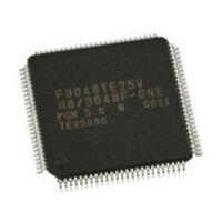
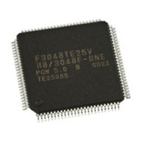
Renesas H8 Series Manuals
Manuals and User Guides for Renesas H8 Series. We have
6
Renesas H8 Series manuals available for free PDF download: Hardware Manual, User Manual
Renesas H8 Series Hardware Manual (697 pages)
8-Bit Single-Chip Microcomputer
Brand:
Renesas
| Category:
Computer Hardware
| Size: 4.21 MB
Table of Contents
Table of Contents
31
Section 1 Overview
43
Overview
43
Internal Block Diagram
49
Pin Arrangement and Functions
51
Pin Arrangement
51
Pin Functions
61
Section 2 CPU
67
Overview
67
Features
67
Address Space
68
Register Configuration
68
Register Descriptions
69
General Registers
69
Control Registers
69
Initial Register Values
71
Data Formats
71
Data Formats in General Registers
72
Memory Data Formats
73
Addressing Modes
74
Effective Address Calculation
76
Instruction Set
80
Data Transfer Instructions
82
Arithmetic Operations
84
Logic Operations
85
Shift Operations
86
Bit Manipulations
88
Branching Instructions
92
System Control Instructions
94
Block Data Transfer Instruction
95
Basic Operational Timing
97
Access to On-Chip Memory (RAM, ROM)
97
Access to On-Chip Peripheral Modules
98
CPU States
99
Overview
99
Program Execution State
101
Program Halt State
101
Exception-Handling State
101
Memory Map
102
Application Notes
108
Notes on Data Access
108
Notes on Bit Manipulation
110
Notes on Use of the EEPMOV Instruction
116
Section 3 Exception Handling
117
Overview
117
Reset
117
Reset Sequence
117
Interrupt Immediately after Reset
118
Interrupts
119
Overview
119
Interrupt Control Registers
121
External Interrupts
132
Internal Interrupts
133
Interrupt Operations
134
Interrupt Response Time
139
Application Notes
140
Notes on Stack Area Use
140
Notes on Rewriting Port Mode Registers
141
Method for Clearing Interrupt Request Flags
143
Section 4 Clock Pulse Generators
145
Overview
145
Block Diagram
145
System Clock and Subclock
146
Register Descriptions
147
System Clock Generator
148
Subclock Generator
153
Prescalers
155
Note on Oscillators
156
Definition of Oscillation Stabilization Wait Time
157
Notes on Use of Crystal Oscillator Element (Excluding Ceramic Oscillator Element)
159
Note on Use of HD64F38024
160
Notes on H8/38124 Group
160
Section 5 Power-Down Modes
161
Overview
161
System Control Registers
164
Sleep Mode
168
Transition to Sleep Mode
168
Clearing Sleep Mode
169
Clock Frequency in Sleep (Medium-Speed) Mode
169
Standby Mode
170
Transition to Standby Mode
170
Clearing Standby Mode
170
Oscillator Stabilization Time after Standby Mode Is Cleared
170
Standby Mode Transition and Pin States
172
Notes on External Input Signal Changes Before/After Standby Mode
173
Watch Mode
174
Transition to Watch Mode
174
Clearing Watch Mode
175
Oscillator Stabilizationtime after Watch Mode Is Cleared
175
Notes on External Input Signal Changes Before/After Watch Mode
175
Subsleep Mode
176
Transition to Subsleep Mode
176
Clearing Subsleep Mode
176
Subactive Mode
177
Transition to Subactive Mode
177
Clearing Subactive Mode
177
Operating Frequency in Subactive Mode
177
Active (Medium-Speed) Mode
178
Transition to Active (Medium-Speed) Mode
178
Clearing Active (Medium-Speed) Mode
178
Operating Frequency in Active (Medium-Speed) Mode
178
Direct Transfer
179
Overview of Direct Transfer
179
Direct Transition Times
180
Notes on External Input Signal Changes Before/After Direct Transition
182
Module Standby Mode
183
Setting Module Standby Mode
183
Clearing Module Standby Mode
183
Section 6 ROM
185
Overview
185
Block Diagram
185
H8/38024 PROM Mode
186
Setting to PROM Mode
186
Socket Adapter Pin Arrangement and Memory Map
186
H8/38024 Programming
189
Writing and Verifying
189
Programming Precautions
194
Reliability of Programmed Data
195
Flash Memory Overview
196
Features
196
Block Diagram
197
Block Configuration
198
Register Configuration
200
Descriptions of Registers of the Flash Memory
200
Flash Memory Control Register 1 (FLMCR1)
200
Flash Memory Control Register 2 (FLMCR2)
203
Erase Block Register (EBR)
204
Flash Memory Power Control Register (FLPWCR)
204
Flash Memory Enable Register (FENR)
205
On-Board Programming Modes
206
Boot Mode
206
Programming/Erasing in User Program Mode
209
Notes on On-Board Programming
210
Flash Memory Programming/Erasing
210
Program/Program-Verify
210
Erase/Erase-Verify
214
Interrupt Handling When Programming/Erasing Flash Memory
214
Program/Erase Protection
216
Hardware Protection
216
Software Protection
216
Error Protection
217
Programmer Mode
217
Socket Adapter
217
Programmer Mode Commands
218
Memory Read Mode
221
Auto-Program Mode
224
Auto-Erase Mode
226
Status Read Mode
227
Status Polling
229
Programmer Mode Transition Time
230
Notes on Memory Programming
230
Power-Down States for Flash Memory
231
Advertisement
Renesas H8 Series Hardware Manual (442 pages)
16-Bit Single-Chip Microcomputer
Brand:
Renesas
| Category:
Computer Hardware
| Size: 2.49 MB
Table of Contents
Table of Contents
11
Section 1 Overview
31
Features
31
Section 1 Overview
32
Figure 1.1 Internal Block Diagram of H8/36912 Group
33
Internal Block Diagram
33
Figure 1.2 Internal Block Diagram of H8/36902 Group
34
Pin Arrangement
35
Figure 1.3 Pin Arrangement of H8/36912 Group (FP-32A)
35
Figure 1.4 Pin Arrangement of H8/36902 Group (FP-32A)
36
Figure 1.5 Pin Arrangement of H8/36912 Group (FP-32D, 32P4B)
37
Figure 1.6 Pin Arrangement of H8/36902 Group (FP-32D, 32P4B)
38
Table 1.1 Pin Functions
39
Pin Functions
39
Section 2 CPU
41
Address Space and Memory Map
42
Figure 2.1 Memory Map (1)
42
Section 2 CPU
42
Figure 2.1 Memory Map (2)
43
Register Configuration
44
Figure 2.2 CPU Registers
44
Figure 2.3 Usage of General Registers
45
General Registers
45
Condition-Code Register (CCR)
46
Figure 2.4 Relationship between Stack Pointer and Stack Area
46
Program Counter (PC)
46
Data Formats
48
General Register Data Formats
48
Figure 2.5 General Register Data Formats (1)
48
Figure 2.5 General Register Data Formats (2)
49
Memory Data Formats
50
Figure 2.6 Memory Data Formats
50
Instruction Set
51
Table of Instructions Classified by Function
51
Table 2.1 Operation Notation
51
Table 2.2 Data Transfer Instructions
52
Table 2.3 Arithmetic Operations Instructions (1)
53
Table 2.3 Arithmetic Operations Instructions (2)
54
Table 2.4 Logic Operations Instructions
55
Table 2.5 Shift Instructions
55
Table 2.6 Bit Manipulation Instructions (1)
56
Table 2.6 Bit Manipulation Instructions (2)
57
Table 2.7 Branch Instructions
58
Table 2.8 System Control Instructions
59
Basic Instruction Formats
60
Table 2.9 Block Data Transfer Instructions
60
Figure 2.7 Instruction Formats
61
Addressing Modes and Effective Address Calculation
62
Addressing Modes
62
Table 2.10 Addressing Modes
62
Table 2.11 Absolute Address Access Ranges
64
Effective Address Calculation
65
Figure 2.8 Branch Address Specification in Memory Indirect Mode
65
Table 2.12 Effective Address Calculation (1)
65
Table 2.12 Effective Address Calculation (2)
66
Basic Bus Cycle
67
Access to On-Chip Memory (RAM, ROM)
67
Figure 2.9 On-Chip Memory Access Cycle
67
On-Chip Peripheral Modules
68
Figure 2.10 On-Chip Peripheral Module Access Cycle (3-State Access)
68
Figure 2.11 CPU Operation States
69
CPU States
69
Usage Notes
70
Notes on Data Access to Empty Areas
70
EEPMOV Instruction
70
Bit Manipulation Instruction
70
Figure 2.12 State Transitions
70
Figure 2.13 Example of Timer Configuration with Two Registers Allocated to same
71
Table 3.1 Exception Sources and Vector Address
77
Section 3 Exception Handling
77
Exception Sources and Vector Address
77
Register Descriptions
79
Interrupt Edge Select Register 1 (IEGR1)
79
Interrupt Edge Select Register 2 (IEGR2)
80
Interrupt Enable Register 1 (IENR1)
80
Interrupt Enable Register 2 (IENR2)
81
Interrupt Flag Register 1 (IRR1)
82
Interrupt Flag Register 2 (IRR2)
83
Wakeup Interrupt Flag Register (IWPR)
83
Reset Exception Handling
84
Interrupt Exception Handling
85
External Interrupts
85
Internal Interrupts
86
Figure 3.1 Reset Sequence
86
Interrupt Handling Sequence
87
Figure 3.2 Stack Status after Exception Handling
88
Interrupt Response Time
89
Table 3.2 Interrupt Wait States
89
Figure 3.3 Interrupt Sequence
90
Usage Notes
91
Interrupts after Reset
91
Notes on Stack Area Use
91
Notes on Rewriting Port Mode Registers
91
Figure 3.4 Port Mode Register Setting and Interrupt Request Flag Clearing Procedure
91
Section 4 Address Break
93
Figure 4.1 Block Diagram of Address Break
93
Register Descriptions
94
Address Break Control Register (ABRKCR)
94
Address Break Status Register (ABRKSR)
96
Break Address Registers (BARH, BARL)
96
Break Data Registers (BDRH, BDRL)
96
Operation
97
Figure 4.2 Address Break Interrupt Operation Example (1)
97
Figure 4.2 Address Break Interrupt Operation Example (2)
98
Figure 5.1 Block Diagram of Clock Pulse Generators
99
Section 5 Clock Pulse Generators
99
Features
100
Register Descriptions
101
RC Control Register (RCCR)
101
RC Trimming Data Protect Register (RCTRMDPR)
102
RC Trimming Data Register (RCTRMDR)
103
Clock Control/Status Register (CKCSR)
104
System Clock Select Operation
105
Figure 5.2 State Transition of System Clock
105
Clock Control Operation
106
Figure 5.3 Flowchart of Clock Switching On-Chip Oscillator Clock to External Clock (1)
106
Figure 5.4 Flowchart of Clock Switching External Clock to On-Chip Oscillator Clock (2)
107
Clock Change Timing
108
Figure 5.5 Timing Chart of Switching On-Chip Oscillator Clock to External Clock
108
Figure 5.6 Timing Chart to Switch External Clock to On-Chip Oscillator Clock
109
Figure 5.7 Example of Trimming Flow for On-Chip Oscillator Frequency
110
Trimming of On-Chip Oscillator Frequency
110
Figure 5.8 Timing Chart of Trimming of On-Chip Oscillator Frequency
111
External Oscillators
112
Connecting Crystal Resonator
112
Figure 5.9 Example of Connection to Crystal Resonator
112
Figure 5.10 Equivalent Circuit of Crystal Resonator
112
Table 5.1 Crystal Resonator Parameters
112
Connecting Ceramic Resonator
113
External Clock Input Method
113
Prescaler
113
Prescaler S
113
Figure 5.11 Example of Connection to Ceramic Resonator
113
Figure 5.12 Example of External Clock Input
113
Usage Notes
114
Note on Resonators
114
Notes on Board Design
114
Figure 5.13 Example of Incorrect Board Design
114
Section 6 Power-Down Modes
115
Register Descriptions
115
System Control Register 1 (SYSCR1)
116
Table 6.1 Operating Frequency and Wait Time
117
System Control Register 2 (SYSCR2)
118
Module Standby Control Register 1 (MSTCR1)
119
Module Standby Control Register 2 (MSTCR2)
120
Mode Transitions and States of LSI
121
Figure 6.1 Mode Transition Diagram
121
Table 6.2 Transition Mode after SLEEP Instruction Execution and Interrupt Handling
122
Table 6.3 Internal State in each Operating Mode
122
Sleep Mode
123
Standby Mode
123
Subsleep Mode
124
Operating Frequency in Active Mode
124
Direct Transition
124
Module Standby Function
125
Section 7 ROM
127
Block Configuration
127
Figure 7.1 Flash Memory Block Configuration
128
Register Descriptions
129
Flash Memory Control Register 1 (FLMCR1)
129
Flash Memory Control Register 2 (FLMCR2)
130
Erase Block Register 1 (EBR1)
131
Flash Memory Enable Register (FENR)
131
On-Board Programming Modes
132
Boot Mode
132
Table 7.1 Setting Programming Modes
132
Table 7.2 Boot Mode Operation
134
Table 7.3 System Clock Frequencies for Which Automatic Adjustment of LSI Bit Rate Is Possible
135
Programming/Erasing in User Program Mode
136
Figure 7.2 Programming/Erasing Flowchart Example in User Program Mode
136
Flash Memory Programming/Erasing
137
Program/Program-Verify
137
Figure 7.3 Program/Program-Verify Flowchart
138
Erase/Erase-Verify
139
Table 7.4 Reprogram Data Computation Table
139
Table 7.5 Additional-Program Data Computation Table
139
Table 7.6 Programming Time
139
Interrupt Handling When Programming/Erasing Flash Memory
140
Figure 7.4 Erase/Erase-Verify Flowchart
141
Program/Erase Protection
142
Hardware Protection
142
Software Protection
142
Error Protection
142
Section 8 RAM
145
Section 9 I/O Ports
147
Port 1
147
Figure 9.1 Port 1 Pin Configuration
147
Port Mode Register 1 (PMR1)
148
Port Control Register 1 (PCR1)
149
Port Data Register 1 (PDR1)
149
Pin Functions
150
Port Pull-Up Control Register 1 (PUCR1)
150
Port 2
151
Figure 9.2 Port 2 Pin Configuration
151
Port Control Register 2 (PCR2)
152
Port Data Register 2 (PDR2)
152
Pin Functions
153
Renesas H8 Series Hardware Manual (434 pages)
16-Bit Single-Chip Microcomputer
Brand:
Renesas
| Category:
Computer Hardware
| Size: 2.67 MB
Table of Contents
General Precautions on Handling of Product
6
Preface
8
Table of Contents
11
Section 1 Overview
31
Features
31
Section 1 Overview
32
Internal Block Diagram
33
Figure 1.1 Internal Block Diagram of H8/36094 Group of F-ZTAT TM
33
Pin Assignments
34
Figure 1.2 Pin Assignments of H8/36094 Group of F-ZTAT TM (FP-64K, FP-64A)
34
Figure 1.3 Pin Assignments of H8/36094 Group of F-ZTAT TM (FP-48F, FP-48B, TNP-48)
35
Overview
35
Pin Functions
36
Table 1.1 Pin Functions
36
Section 2 CPU
39
Address Space and Memory Map
40
Figure 2.1 Memory Map
40
Register Configuration
41
Figure 2.2 CPU Registers
41
Figure 2.3 Usage of General Registers
42
General Registers
42
Appendix
43
Condition-Code Register (CCR)
43
Figure 2.4 Relationship between Stack Pointer and Stack Area
43
Program Counter (PC)
43
Data Formats
45
General Register Data Formats
45
Figure 2.5 General Register Data Formats (1)
45
Figure 2.5 General Register Data Formats (2)
46
Memory Data Formats
47
Figure 2.6 Memory Data Formats
47
Instruction Set
48
Table of Instructions Classified by Function
48
Table 2.1 Operation Notation
48
Table 2.2 Data Transfer Instructions
49
Table 2.3 Arithmetic Operations Instructions (1)
50
Table 2.3 Arithmetic Operations Instructions (2)
51
Table 2.4 Logic Operations Instructions
52
Table 2.5 Shift Instructions
52
Table 2.6 Bit Manipulation Instructions (1)
53
Table 2.6 Bit Manipulation Instructions (2)
54
Table 2.7 Branch Instructions
55
Table 2.8 System Control Instructions
56
Basic Instruction Formats
57
Table 2.9 Block Data Transfer Instructions
57
Addressing Modes and Effective Address Calculation
58
Addressing Modes
58
Figure 2.7 Instruction Formats
58
Table 2.10 Addressing Modes
59
Table 2.11 Absolute Address Access Ranges
60
Figure 2.8 Branch Address Specification in Memory Indirect Mode
61
Effective Address Calculation
62
Table 2.12 Effective Address Calculation (1)
62
Table 2.12 Effective Address Calculation (2)
63
Basic Bus Cycle
64
Access to On-Chip Memory (RAM, ROM)
64
Figure 2.9 On-Chip Memory Access Cycle
64
On-Chip Peripheral Modules
65
Figure 2.10 On-Chip Peripheral Module Access Cycle (3-State Access)
65
CPU States
66
Figure 2.11 CPU Operation States
66
Usage Notes
67
Notes on Data Access to Empty Areas
67
EEPMOV Instruction
67
Bit Manipulation Instruction
67
Figure 2.12 State Transitions
67
Figure 2.13 Example of Timer Configuration with Two Registers Allocated to same
68
Section 3 Exception Handling
73
Exception Sources and Vector Address
73
Table 3.1 Exception Sources and Vector Address
73
Register Descriptions
75
Interrupt Edge Select Register 1 (IEGR1)
75
Interrupt Edge Select Register 2 (IEGR2)
76
Interrupt Enable Register 1 (IENR1)
77
Interrupt Flag Register 1 (IRR1)
78
Wakeup Interrupt Flag Register (IWPR)
79
Reset Exception Handling
81
Interrupt Exception Handling
81
External Interrupts
81
Figure 3.1 Reset Sequence
82
Internal Interrupts
83
Interrupt Handling Sequence
83
Interrupt Response Time
84
Figure 3.2 Stack Status after Exception Handling
84
Table 3.2 Interrupt Wait States
84
Figure 3.3 Interrupt Sequence
85
Usage Notes
86
Interrupts after Reset
86
Notes on Stack Area Use
86
Notes on Rewriting Port Mode Registers
86
Figure 3.4 Port Mode Register Setting and Interrupt Request Flag Clearing Procedure
86
Section 4 Address Break
87
Register Descriptions
87
Figure 4.1 Block Diagram of Address Break
87
Address Break Control Register (ABRKCR)
88
Address Break Status Register (ABRKSR)
89
Table 4.1 Access and Data Bus Used
89
Break Address Registers (BARH, BARL)
90
Break Data Registers (BDRH, BDRL)
90
Operation
90
Figure 4.2 Address Break Interrupt Operation Example (1)
91
Figure 4.2 Address Break Interrupt Operation Example (2)
91
Section 5 Clock Pulse Generators
93
Figure 5.1 Block Diagram of Clock Pulse Generators
93
Features
94
Register Descriptions
94
RC Control Register (RCCR)
95
RC Trimming Data Protect Register (RCTRMDPR)
96
RC Trimming Data Register (RCTRMDR)
97
Clock Control/Status Register (CKCSR)
98
System Clock Select Operation
100
Figure 5.2 State Transition of System Clock
100
Clock Control Operation
101
Figure 5.3 Flowchart of Clock Switching with Backup Function Enabled
101
Figure 5.4 Flowchart of Clock Switching with Backup Function Disabled (1) (from On-Chip Oscillator Clock to External Clock)
102
Figure 5.5 Flowchart of Clock Switching with Backup Function Disabled (2) (from External Clock to On-Chip Oscillator Clock)
103
Clock Switching Timing
104
Figure 5.6 Timing Chart of Switching from On-Chip Oscillator Clock to External Clock
104
Figure 5.7 Timing Chart to Switch from External Clock to On-Chip Oscillator Clock
105
Figure 5.8 External Oscillation Backup Timing
106
Trimming of On-Chip Oscillator Frequency
107
Figure 5.9 Example of Trimming Flow for On-Chip Oscillator Clock
107
Figure 5.10 Timing Chart of Trimming of On-Chip Oscillator Frequency
108
External Clock Oscillators
109
Connecting Crystal Resonator
109
Figure 5.11 Example of Connection to Crystal Resonator
109
Figure 5.12 Equivalent Circuit of Crystal Resonator
109
Table 5.1 Crystal Resonator Parameters
109
Connecting Ceramic Resonator
110
Inputting External Clock
110
Figure 5.13 Example of Connection to Ceramic Resonator
110
Figure 5.14 Example of External Clock Input
110
Subclock Oscillator
111
Connecting 32.768-Khz Crystal Resonator
111
Figure 5.15 Block Diagram of Subclock Oscillator
111
Figure 5.16 Typical Connection to 32.768-Khz Crystal Resonator
111
Figure 5.17 Equivalent Circuit of 32.768-Khz Crystal Resonator
111
Pin Connection When Not Using Subclock
112
Prescaler
112
Prescaler S
112
Prescaler W
112
Figure 5.18 Pin Connection When Not Using Subclock
112
Usage Notes
113
Note on Resonators
113
Notes on Board Design
113
Figure 5.19 Example of Incorrect Board Design
113
Section 6 Power-Down Modes
115
Register Descriptions
115
System Control Register 1 (SYSCR1)
115
System Control Register 2 (SYSCR2)
117
Table 6.1 Operating Frequency and Waiting Time
117
Module Standby Control Register 1 (MSTCR1)
118
Mode Transitions and States of LSI
119
Figure 6.1 Mode Transition Diagram
119
Table 6.2 Transition Mode after SLEEP Instruction Execution and Interrupt Handling
120
Table 6.3 Internal State in each Operating Mode
121
Sleep Mode
122
Standby Mode
122
Subactive Mode
123
Subsleep Mode
123
Operating Frequency in Active Mode
124
Direct Transition
124
Direct Transition from Active Mode to Subactive Mode
124
Direct Transition from Subactive Mode to Active Mode
125
Module Standby Function
125
Section 7 ROM
127
Block Configuration
128
Figure 7.1 Flash Memory Block Configuration
128
Register Descriptions
129
Flash Memory Control Register 1 (FLMCR1)
129
Flash Memory Control Register 2 (FLMCR2)
130
Erase Block Register 1 (EBR1)
131
Flash Memory Power Control Register (FLPWCR)
132
Flash Memory Enable Register (FENR)
132
On-Board Programming Modes
133
Boot Mode
133
Table 7.1 Setting Programming Modes
133
Table 7.2 Boot Mode Operation
135
Programming/Erasing in User Program Mode
136
Figure 7.2 Programming/Erasing Flowchart Example in User Program Mode
136
Table 7.3 System Clock Frequencies for Which Automatic Adjustment of LSI Bit Rate Is Possible
136
Flash Memory Programming/Erasing
137
Program/Program-Verify
137
Figure 7.3 Program/Program-Verify Flowchart
138
Erase/Erase-Verify
139
Table 7.4 Reprogram Data Computation Table
139
Table 7.5 Additional-Program Data Computation Table
139
Table 7.6 Programming Time
139
Interrupt Handling When Programming/Erasing Flash Memory
140
Figure 7.4 Erase/Erase-Verify Flowchart
141
Program/Erase Protection
142
Hardware Protection
142
Software Protection
142
Error Protection
142
Programmer Mode
143
Power-Down States for Flash Memory
143
Table 7.7 Flash Memory Operating States
143
Advertisement
Renesas H8 Series User Manual (408 pages)
16-Bit Single-Chip Microcomputer
Brand:
Renesas
| Category:
Computer Hardware
| Size: 3.85 MB
Table of Contents
General Precautions on Handling of Product
4
Preface
6
Table of Contents
9
Appendix
24
Section 1 Overview
29
Features
29
Internal Block Diagram
31
Figure 1.1 Internal Block Diagram of H8/36912 Group
31
Figure 1.2 Internal Block Diagram of H8/36902 Group
32
Section 2 CPU
32
Section 2 CPU
31
Figure 1.3 Pin Arrangement of H8/36912 Group (LQFP-32)
33
Pin Arrangement
33
Figure 1.4 Pin Arrangement of H8/36902 Group (LQFP-32)
34
Figure 1.5 Pin Arrangement of H8/36912 Group (SOP-32)
35
Figure 1.6 Pin Arrangement of H8/36902 Group (SOP-32)
36
Table 1.1 Pin Functions
37
Pin Functions
37
Manual
38
Section 2 CPU
39
Address Space and Memory Map
40
Figure 2.1 Memory Map (1)
40
Figure 2.1 Memory Map (2)
41
Register Configuration
42
Figure 2.2 CPU Registers
42
Figure 2.3 Usage of General Registers
43
General Registers
43
Condition-Code Register (CCR)
44
Figure 2.4 Relationship between Stack Pointer and Stack Area
44
Program Counter (PC)
44
Data Formats
46
General Register Data Formats
46
Figure 2.5 General Register Data Formats (1)
46
Figure 2.5 General Register Data Formats (2)
47
Memory Data Formats
48
Figure 2.6 Memory Data Formats
48
Instruction Set
49
Table of Instructions Classified by Function
49
Table 2.1 Operation Notation
49
Table 2.2 Data Transfer Instructions
50
Table 2.3 Arithmetic Operations Instructions (1)
51
Table 2.3 Arithmetic Operations Instructions (2)
52
Table 2.4 Logic Operations Instructions
52
Table 2.5 Shift Instructions
53
Table 2.6 Bit Manipulation Instructions (1)
55
Table 2.6 Bit Manipulation Instructions (2)
55
Table 2.7 Branch Instructions
56
Table 2.8 System Control Instructions
57
Table 2.9 Block Data Transfer Instructions
57
Basic Instruction Formats
58
Figure 2.7 Instruction Formats
58
Addressing Modes and Effective Address Calculation
59
Addressing Modes
59
Table 2.10 Addressing Modes
59
Table 2.11 Absolute Address Access Ranges
60
Figure 2.8 Branch Address Specification in Memory Indirect Mode
61
Effective Address Calculation
62
Table 2.12 Effective Address Calculation (1)
62
Table 2.12 Effective Address Calculation (2)
63
Basic Bus Cycle
64
Access to On-Chip Memory (RAM, ROM)
64
Figure 2.9 On-Chip Memory Access Cycle
64
On-Chip Peripheral Modules
65
Figure 2.10 On-Chip Peripheral Module Access Cycle (3-State Access)
65
Figure 2.11 CPU Operation States
66
Figure 2.12 State Transitions
66
CPU States
66
Usage Notes
67
Notes on Data Access to Empty Areas
67
EEPMOV Instruction
67
Bit Manipulation Instruction
67
Figure 2.13 Example of Timer Configuration with Two Registers Allocated to same
68
Section 3 Exception Handling
73
Exception Sources and Vector Address
73
Register Descriptions
75
Interrupt Edge Select Register 1 (IEGR1)
75
Interrupt Edge Select Register 2 (IEGR2)
76
Interrupt Enable Register 1 (IENR1)
76
Interrupt Enable Register 2 (IENR2)
77
Interrupt Flag Register 1 (IRR1)
78
Interrupt Flag Register 2 (IRR2)
79
Wakeup Interrupt Flag Register (IWPR)
79
Reset Exception Handling
80
Interrupt Exception Handling
81
External Interrupts
81
Internal Interrupts
82
Interrupt Handling Sequence
82
Figure 3.1 Reset Sequence
82
Figure 3.2 Stack Status after Exception Handling
83
Interrupt Response Time
84
Table 3.2 Interrupt Wait States
84
Figure 3.3 Interrupt Sequence
85
Usage Notes
86
Interrupts after Reset
86
Notes on Stack Area Use
86
Notes on Rewriting Port Mode Registers
86
Figure 3.4 Port Mode Register Setting and Interrupt Request Flag Clearing Procedure
86
Section 4 Address Break
87
Register Descriptions
87
Figure 4.1 Block Diagram of Address Break
87
Address Break Control Register (ABRKCR)
88
Address Break Status Register (ABRKSR)
89
Table 4.1 Access and Data Bus Used
89
Break Address Registers (BARH, BARL)
90
Break Data Registers (BDRH, BDRL)
90
Operation
91
Figure 4.2 Address Break Interrupt Operation Example (1)
91
Figure 4.2 Address Break Interrupt Operation Example (2)
92
Section 5 Clock Pulse Generators
93
Figure 5.1 Block Diagram of Clock Pulse Generators
93
Features
94
Register Descriptions
95
RC Control Register (RCCR)
95
RC Trimming Data Protect Register (RCTRMDPR)
96
RC Trimming Data Register (RCTRMDR)
97
Clock Control/Status Register (CKCSR)
97
System Clock Select Operation
99
Figure 5.2 State Transition of System Clock
99
Clock Control Operation
100
Figure 5.3 Flowchart of Clock Switching with Backup Function Enabled
100
Figure 5.4 Flowchart of Clock Switching with Backup Function Disabled (1) (from Internal RC Clock to External Clock)
101
Figure 5.5 Flowchart of Clock Switching with Backup Function Disabled (2) (from External Clock to Internal RC Clock)
102
Clock Change Timing
103
Figure 5.6 Timing Chart of Switching Internal RC Clock to External Clock
103
Figure 5.7 Timing Chart to Switch External Clock to Internal RC Clock
104
Figure 5.8 External Oscillation Backup Timing
105
Figure 5.9 Example of Trimming Flow for Internal RC Oscillator Frequency
106
Trimming of Internal RC Oscillator Frequency
106
Figure 5.10 Timing Chart of Trimming of Internal RC Oscillator Frequency
107
External Oscillators
108
Connecting Crystal Resonator
108
Figure 5.11 Example of Connection to Crystal Resonator
108
Figure 5.12 Equivalent Circuit of Crystal Resonator
108
Table 5.1 Crystal Resonator Parameters
108
Connecting Ceramic Resonator
109
External Clock Input Method
109
Prescaler
109
Prescaler S
109
Figure 5.13 Example of Connection to Ceramic Resonator
109
Figure 5.14 Example of External Clock Input
109
Usage Notes
110
Note on Resonators
110
Notes on Board Design
110
Figure 5.15 Example of Incorrect Board Design
110
Section 6 Power-Down Modes
111
Register Descriptions
112
System Control Register 1 (SYSCR1)
112
System Control Register 2 (SYSCR2)
114
Module Standby Control Register 1 (MSTCR1)
115
Module Standby Control Register 2 (MSTCR2)
116
Mode Transitions and States of LSI
117
Figure 6.1 Mode Transition Diagram
117
Table 6.2 Transition Mode after SLEEP Instruction Execution and Interrupt Handling
117
Sleep Mode
118
Table 6.3 Internal State in each Operating Mode
118
Standby Mode
119
Subsleep Mode
119
Operating Frequency in Active Mode
120
Direct Transition
120
Module Standby Function
120
Section 7 ROM
121
Block Configuration
122
Figure 7.1 Flash Memory Block Configuration
123
Register Descriptions
124
Flash Memory Control Register 1 (FLMCR1)
124
Flash Memory Control Register 2 (FLMCR2)
125
Erase Block Register 1 (EBR1)
126
Flash Memory Enable Register (FENR)
126
On-Board Programming Modes
127
Boot Mode
127
Table 7.1 Setting Programming Modes
127
Table 7.2 Boot Mode Operation
129
Programming/Erasing in User Program Mode
130
Figure 7.2 Programming/Erasing Flowchart Example in User Program Mode
130
Table 7.3 System Clock Frequencies for Which Automatic Adjustment of LSI Bit Rate Is
130
Flash Memory Programming/Erasing
131
Program/Program-Verify
131
Figure 7.3 Program/Program-Verify Flowchart
132
Erase/Erase-Verify
133
Table 7.4 Reprogram Data Computation Table
133
Table 7.5 Additional-Program Data Computation Table
133
Table 7.6 Programming Time
133
Interrupt Handling When Programming/Erasing Flash Memory
134
Figure 7.4 Erase/Erase-Verify Flowchart
135
Program/Erase Protection
136
Hardware Protection
136
Software Protection
136
Error Protection
136
Section 8 RAM
137
Section 9 I/O Ports
139
Port 1
139
Figure 9.1 Port 1 Pin Configuration
139
Port Mode Register 1 (PMR1)
140
Port Control Register 1 (PCR1)
141
Port Data Register 1 (PDR1)
141
Pin Functions
142
Port Pull-Up Control Register 1 (PUCR1)
142
Renesas H8 Series Hardware Manual (551 pages)
8-Bit Single-Chip Microcomputer
Brand:
Renesas
| Category:
Computer Hardware
| Size: 3.63 MB
Table of Contents
Table of Contents
13
Section 1 Overview
23
Overview
23
Internal Block Diagram
28
Pin Arrangement and Functions
29
Pin Arrangement
29
Pin Functions
32
Section 2 CPU
37
Overview
37
Features
37
Address Space
38
Register Configuration
38
Register Descriptions
40
General Registers
40
Control Registers
40
Initial Register Values
42
Data Formats
42
Data Formats in General Registers
43
Memory Data Formats
44
Addressing Modes
45
Effective Address Calculation
47
Instruction Set
51
Data Transfer Instructions
53
Arithmetic Operations
55
Logic Operations
56
Shift Operations
56
Bit Manipulations
58
Branching Instructions
62
System Control Instructions
64
Block Data Transfer Instruction
65
Basic Operational Timing
66
Access to On-Chip Memory (RAM, ROM)
66
Access to On-Chip Peripheral Modules
67
CPU States
68
Overview
68
Program Execution State
70
Program Halt State
70
Exception-Handling State
70
Memory Map
71
Application Notes
72
Notes on Data Access
72
Notes on Bit Manipulation
74
Notes on Use of the EEPMOV Instruction
80
Section 3 Exception Handling
81
Overview
81
Reset
81
Reset Sequence
81
Interrupt Immediately after Reset
83
Interrupts
83
Overview
83
Interrupt Control Registers
85
External Interrupts
93
Internal Interrupts
94
Interrupt Operations
94
Interrupt Response Time
99
Application Notes
100
Notes on Stack Area Use
100
Notes on Rewriting Port Mode Registers
101
Section 4 Clock Pulse Generators
103
Overview
103
Block Diagram
103
System Clock and Subclock
103
System Clock Generator
104
Subclock Generator
106
Prescalers
107
Note on Oscillators
108
Section 5 Power-Down Modes
109
Overview
109
System Control Registers
112
Sleep Mode
116
Transition to Sleep Mode
116
Clearing Sleep Mode
116
Clock Frequency in Sleep (Medium-Speed) Mode
117
Standby Mode
117
Transition to Standby Mode
117
Clearing Standby Mode
117
Oscillator Settling Time after Standby Mode Is Cleared
118
Watch Mode
118
Transition to Watch Mode
118
Clearing Watch Mode
119
Oscillator Settling Time after Watch Mode Is Cleared
119
Subsleep Mode
119
Transition to Subsleep Mode
119
Clearing Subsleep Mode
120
Subactive Mode
120
Transition to Subactive Mode
120
Clearing Subactive Mode
120
Operating Frequency in Subactive Mode
121
Active (Medium-Speed) Mode
121
Transition to Active (Medium-Speed) Mode
121
Clearing Active (Medium-Speed) Mode
121
Operating Frequency in Active (Medium-Speed) Mode
121
Direct Transfer
122
Section 6 ROM
125
Overview
125
Block Diagram
125
PROM Mode
126
Setting to PROM Mode
126
Memory Map
126
Programming
127
Writing and Verifying
128
Programming Precautions
131
Reliability of Programmed Data
132
Flash Memory Overview
133
Principle of Flash Memory Operation
133
Mode Pin Settings and ROM Space
134
Features
134
Block Diagram
135
Pin Configuration
136
Register Configuration
136
Renesas H8 Series User Manual (272 pages)
Microcomputer Development Environment System
Brand:
Renesas
| Category:
Computer Hardware
| Size: 2.25 MB
Table of Contents
Table of Contents
15
Emulator Debugger Part
21
Section 1 Overview
23
Features
23
Warnings
24
Environmental Conditions
25
Emulator External Dimensions and Mass
25
Section 2 Preparation before Use
27
Emulator Preparation
27
Installing Emulator's Software
27
Connecting to the User System
28
Example of Connecting the User System Interface Cable Head to the User System
28
Plugging the User System Interface Cable Body into the Emulator
29
Plugging the User System Interface Cable Body into the Cable Head
29
Power Supply
30
AC Adapter
30
Polarity
30
Power Supply Monitor Circuit
30
SIMM Memory Module
30
Optional SIMM Memory Module Configuration
30
Hardware Interface
31
Signal Protection on the Emulator
31
User System Interface Circuits
31
Clock Oscillator
31
External Probe 1 (Ext1)/Trigger Output
31
External Probe 2 (Ext2)/Trigger Output
32
Voltage Follower Circuit
33
System Check
34
Communication Problems
39
Other Methods for Activating the Emulator
39
Uninstalling the Emulator's Software
39
Section 3 E6000 Emulator Functions
41
Debugging Features
41
Breakpoints
41
Trace
41
Execution Time Measurements
41
Performance Analysis
41
Bus Monitoring
42
Complex Event System (CES)
42
Event Channels
42
Range Channels
43
Breaks
43
Timing
43
Hardware Features
44
Memory
44
Clocks
45
Probes
45
Stack Trace Function
45
Online Help
45
Section 4 Preparation before Use
47
Method for Activating High-Performance Embedded Workshop
47
Creating a New Workspace (Toolchain Not Used)
48
Creating a New Workspace (Toolchain Used)
52
Selecting an Existing Workspace
56
Connecting the Emulator
57
Reconnecting the Emulator
58
Ending the Emulator
58
Section 5 Debugging
59
Setting the Environment for Emulation
60
Opening the [Configuration Properties] Dialog Box
60
Selecting an MCU Not Included in the List
62
Selecting the Interface to be Connected
63
Opening the [Memory Mapping] Dialog Box
64
Changing the Memory Map Setting
65
Downloading a Program
66
Viewing the Source Code
67
Viewing the Assembly-Language Code
70
Modifying the Assembly-Language Code
71
Viewing a Specific Address
71
Viewing the Current Program Counter Address
71
Viewing the Current Status
72
Reading and Displaying the Emulator Information Regularly
73
Advertisement
Related Products
Renesas H8/3001
Renesas H8/330
Renesas H8/3337Y
Renesas H8/338
Renesas H8/3334
Renesas H8/350
Renesas H8/33937
Renesas H8/3937R
Renesas H8/38347
Renesas H8S/2168
Renesas Categories
Computer Hardware
Motherboard
Microcontrollers
Adapter
Switch
More Renesas Manuals
Login
Sign In
OR
Sign in with Facebook
Sign in with Google
Upload manual
Upload from disk
Upload from URL