Table of Contents
Advertisement
Quick Links
Download this manual
See also:
User Manual
Advertisement
Table of Contents

Related Manuals for Xilinx AC701


Summary of Contents for Xilinx AC701
- Page 1 AC701 Evaluation Board for the Artix-7 FPGA User Guide UG952 (v1.4) August 6, 2019...
-
Page 2: Revision History
Xilinx’s limited warranty, please refer to Xilinx’s Terms of Sale which can be viewed at https://www.xilinx.com/legal.htm#tos; IP cores may be subject to warranty and support terms contained in a license issued to you by Xilinx. Xilinx products are not designed or intended to be fail-safe or for use in any application requiring fail-safe performance;... - Page 3 XADC_GPIO_3, 2, 1, 0 description in Table 1-35. Added Figure A-3 to show board components called out in Table A-3. Updated the Artix-7 FPGA AC701 Declaration of Conformity link in Appendix F, Regulatory and Compliance Information. 08/06/2019 Updated DDR3 Memory Module section.
- Page 4 AC701 Evaluation Board www.xilinx.com UG952 (v1.4) August 6, 2019...
-
Page 5: Table Of Contents
AC701 Board Power System ........ - Page 6 Appendix D: Board Setup Installing the AC701 Board in a PC Chassis ........89...
-
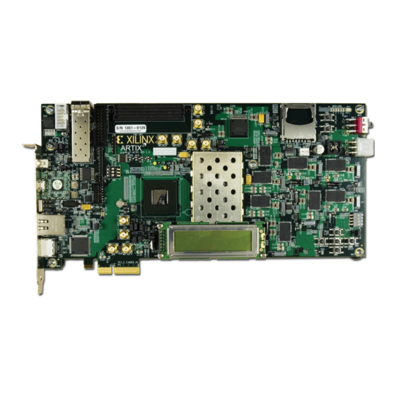
Page 7: Chapter 1: Ac701 Evaluation Board Features
AC701 Evaluation Board Features Overview The AC701 evaluation board for the Artix®-7 FPGA provides a hardware environment for developing and evaluating designs targeting the Artix-7 XC7A200T-2FBG676C FPGA. The AC701 board provides features common to many embedded processing systems, including a DDR3 SODIMM memory, an 4-lane PCI Express®... - Page 8 Chapter 1: AC701 Evaluation Board Features • Gen2 4-lane (x4) • SFP+ connector • 10/100/1,000 tri-speed Ethernet PHY • USB-to-UART bridge • High-Definition Multimedia Interface (HDMI™) technology codec • I2C bus • I2C MUX • I2C EEPROM (1 KB) •...
-
Page 9: Electrostatic Discharge Caution
• Put the adapter down only on an antistatic surface such as the bag supplied in your kit. • If you are returning the adapter to Xilinx Product Support, place it back in its antistatic bag immediately. • If a wrist strap is not available, ground yourself by touching the metal chassis before handling the adapter or any other part of the computer/server. - Page 10 1 KB EEPROM (I 2 C) DIP Switch SW1 JTAG Interface USB-to-UART Bridge SFP+ Single Cage I 2 C Bus Switch micro-B USB Connector Config UG952_c1_01_101512 Figure 1-1: AC701 Board Block Diagram www.xilinx.com AC701 Evaluation Board Send Feedback UG952 (v1.4) August 6, 2019...
-
Page 11: Feature Descriptions
Feature Descriptions Feature Descriptions Figure 1-2 shows the AC701 board. Each numbered feature that is referenced in Figure 1-2 described in the sections that follow. Note: Figure 1-2 The image in is for reference only and might not reflect the current revision of the board. - Page 12 Chapter 1: AC701 Evaluation Board Features Table 1-1: AC701 Board Component Descriptions (Cont’d) Schematic Reference Callout Component Description Notes 0381502 Designator Page Number J25, J26 SMA GTP reference clock input Rosenberger 32K10K-400L5 Jitter attenuated clock (back side of board) Silicon Labs SI5324-C-GM...
-
Page 13: Artix-7 Fpga
Master SPI flash memory using the onboard Quad SPI flash memory • JTAG using a standard-A to micro-B USB cable for connecting the host PC to the AC701 board configuration port or by J4 Platform Cable USB/Parallel Cable IV flat cable connector... - Page 14 Figure 1-4: Encryption Key Backup Circuit I/O Voltage Rails In addition to Bank 0, there are eight I/O banks available on the Artix-7 device. The voltages applied to the FPGA I/O banks used by the AC701 board are listed in Table 1-3.
-
Page 15: Ddr3 Memory Module
Datapath width: 64 bits • Data rate: up to 1,600 MT/s The AC701 XC7A200T FPGA memory interface performance is documented in the Artix-7 FPGAs Data Sheet: DC and AC Switching Characteristics (DS181) [Ref The DDR3 interface is implemented across I/O banks 33, 34, and 35. An external 0.75V reference VTTREF is provided for these banks. - Page 16 Chapter 1: AC701 Evaluation Board Features Table 1-4: DDR3 Memory Connections to the FPGA (Cont’d) J1 DDR3 Memory Schematic Net FPGA Pin (U1) I/O Standard Name Pin Number Pin Name DDR3_A13 SSTL15 DDR3_A14 SSTL15 DDR3_A15 SSTL15 DDR3_BA0 SSTL15 DDR3_BA1 SSTL15...
- Page 17 SSTL15 DQ48 DDR3_D49 SSTL15 DQ49 DDR3_D50 SSTL15 DQ50 DDR3_D51 SSTL15 DQ51 DDR3_D52 SSTL15 DQ52 DDR3_D53 SSTL15 DQ53 DDR3_D54 SSTL15 DQ54 DDR3_D55 SSTL15 DQ55 DDR3_D56 SSTL15 DQ56 DDR3_D57 SSTL15 DQ57 AC701 Evaluation Board www.xilinx.com Send Feedback UG952 (v1.4) August 6, 2019...
- Page 18 Chapter 1: AC701 Evaluation Board Features Table 1-4: DDR3 Memory Connections to the FPGA (Cont’d) J1 DDR3 Memory Schematic Net FPGA Pin (U1) I/O Standard Name Pin Number Pin Name DDR3_D58 SSTL15 DQ58 DDR3_D59 SSTL15 DQ59 DDR3_D60 SSTL15 DQ60 DDR3_D61...
- Page 19 DIFF_SSTL15 CK1_P The AC701 board DDR3 memory interface adheres to the constraints guidelines documented in the DDR3 Design Guidelines section of the 7 Series FPGAs Memory Interface Solutions User Guide 4]. The AC701 board DDR3 memory interface is a 40 Ω impedance implementation.
-
Page 20: Quad Spi Flash Memory
Quad SPI flash memory. Figure 1-5 shows the connections of the Quad SPI flash memory on the AC701 board. For more details, see the Micron N25Q256A13ESF40G data sheet [Ref 15]. X-Ref Target - Figure 1-5... -
Page 21: Spi Flash Memory External Programming Header
J7 SPI flash memory external programming connector. X-Ref Target - Figure 1-6 FPGA_PROG_B FLASH_D3 FLASH_D2 QSPI_CS_B FLASH_D0 FLASH_D1 VCC3V3 FPGA_CCLK UG952_c1_06_092812 Figure 1-6: SPI Flash Memory J7 External Programming Connector AC701 Evaluation Board www.xilinx.com Send Feedback UG952 (v1.4) August 6, 2019... -
Page 22: Sd Card Interface
[Figure 1-2, callout 4] The AC701 board includes a secure digital input/output (SDIO) interface to provide user-logic access to general purpose nonvolatile SDIO memory cards and peripherals. The SD card slot is designed to support 50 MHz high speed SD cards. -
Page 23: Usb Jtag Module
UG952_c1_08_012913 Figure 1-8: JTAG Chain Block Diagram When an FMC card is attached to the AC701 board, it is automatically added to the JTAG chain through electronically controlled single-pole single-throw (SPST) switch U27. The SPST switch is in a normally closed state and transitions to an open state when an FMC card is attached. Switch U27 adds an attached FMC HPC mezzanine card to the FPGAs JTAG chain as determined by the FMC_HPC_PRSNT_M2C_B signal. -
Page 24: Clock Generation
Chapter 1: AC701 Evaluation Board Features The JTAG connectivity on the AC701 board allows a host computer to download bitstreams to the FPGA using Xilinx software tools. In addition, the JTAG connector allows debug tools or a software debugger to access the FPGA. Xilinx software tools can also indirectly program the Quad SPI flash memory. - Page 25 Feature Descriptions Table 1-8: AC701 Board Clock Sources (Cont’d) FPGA Schematic Net Clock I/O Standard Description Pin (U1) Name Reference USER_CLOCK_P LVDS_25 Si570 3.3V LVDS I2C Programmable Oscillator (Silicon Labs). Default power-on frequency 156.250 MHz. See USER_CLOCK_N LVDS_25 Programmable User Clock Source.
- Page 26 156.250 MHz. User applications can change the output frequency within the range of 10 MHz to 810 MHz through an I2C interface. Power cycling the AC701 board reverts the user clock to its default frequency of 156.250 MHz.
- Page 27 USER_SMA_CLOCK_P/N signals should not exceed the VCCO_VADJ voltage (1.8V, 2.5V or 3.3V) in use. X-Ref Target - Figure 1-13 USER_SMA_CLOCK_P Connector USER_SMA_CLOCK_N Connector UG952_c1_12_100212 Figure 1-13: User SMA Clock Source AC701 Evaluation Board www.xilinx.com Send Feedback UG952 (v1.4) August 6, 2019...
- Page 28 GTP Transceiver Clock Multiplexer [Figure 1-2, callout 35] The AC701 board provides flexible GTP Quad 213 MGTREFCLK options through the use of external multiplexer (MUX) components U3 and U4 to service the GTP Quad 213 SFP, FMC, and SMA MGT interfaces.
- Page 29 Net SFP_MGT_CLK_SEL1 is wired to FPGA U1 pin C24 and net SFP_MGT_CLK_SEL0 is wired to FPGA U1 pin B26 on FPGA U1 Bank 16. The U3 multiplexer circuit is shown in Figure 1-15. AC701 Evaluation Board www.xilinx.com Send Feedback UG952 (v1.4) August 6, 2019...
- Page 30 Chapter 1: AC701 Evaluation Board Features X-Ref Target - Figure 1-15 VCC2V5 VCC2V5 SY89544UMG C105 0.1μF VCC1 VCC3 VCC2 VCC4 EPHYCLK_Q0_P VCC5 VCC6 C320 EPHYCLK_Q0_N VCC7 0.1μF SI5324_OUT0_C_P VCC8 SFP_MGT_CLK0_P SI5324_OUT0_C_N SFP_MGT_CLK0_P FMC1_HBC_GBTCLK0_M2C_C_P C318 TO MGT BANK 213 GND1 0.1μF...
- Page 31 Net PCIE_MGT_CLK_SEL1 is wired to FPGA U1 pin C26 and net PCIE_MGT_CLK_SEL0 is wired to FPGA U1 pin A24 on FPGA U1 Bank 16. The U4 Multiplexer circuit is shown in Figure 1-16. AC701 Evaluation Board www.xilinx.com Send Feedback UG952 (v1.4) August 6, 2019...
- Page 32 Chapter 1: AC701 Evaluation Board Features X-Ref Target - Figure 1-16 VCC2V5 VCC2V5 SY89544UMG C106 0.1μF VCC1 VCC3 VCC2 VCC4 SMA_MGT_REFCLK_P VCC5 VCC6 C321 SMA_MGT_REFCLK_N VCC7 0.1μF SI5324_OUT1_C_P VCC8 SFP_MGT_CLK1_P SI5324_OUT1_C_N SFP_MGT_CLK1_P FMC1_HBC_GBTCLK1_M2C_C_P C322 GND1 TO MGT BANK 213 0.1μF...
- Page 33 GND1 1.0M 5% EPHYCLK_Q0_C_N EPHYCLK_Q0_N EPHYCLK_XTAL_IN XTAL_IN GND2 R487 0Ω 5% C301 18pF 50V GND_EPHYCLK GND_EPHYCLK GND_EPHYCLK UG952_c1_13_101512 Figure 1-17: AC701 Board 125 MHz U3 MUX IN0 Source Circuit AC701 Evaluation Board www.xilinx.com Send Feedback UG952 (v1.4) August 6, 2019...
- Page 34 [Figure 1-2, callout 10] The AC701 board includes a Silicon Labs Si5324 jitter attenuator U24 on the back side of the board. FPGA user logic can implement a clock recovery circuit and then output this clock to a differential I/O pair on I/O bank 16 (REC_CLOCK_C_P, FPGA U1 pin D23 and REC_CLOCK_C_N, FPGA U1 pin D24) for jitter attenuation.
-
Page 35: Gtp Transceivers
[Figure 1-2, callout 9] The AC701 board includes a pair of SMA connectors for a GTP transceiver clock that are wired to GTP quad bank 213 through clock MUX U4. This differential clock has signal names SMA_MGT_REFCLK_P and SMA_REFCLK_N, which are connected to MGT clock MUX U4 input 0 pins 4 and 2 respectively. - Page 36 The GTP transceivers in 7 series FPGAs are grouped into four channels described as Quads. The reference clock for a Quad can be sourced from the Quad above or Quad below the GTP Quad of interest. There are two GTP transceiver Quads on the AC701 board with connectivity as shown here: •...
- Page 37 2. PCIE_TXn_P/N and PCIE_CLK_Q0_P/N are capacitively coupled to the PCIe edge connector P1. For more information on the GTP transceivers see 7 Series FPGAs GTX/GTH Transceivers User Guide (UG476) [Ref AC701 Evaluation Board www.xilinx.com Send Feedback UG952 (v1.4) August 6, 2019...
-
Page 38: Pci Express Edge Connector
85Ω ±10%. The PCIe clock is routed as a 100Ω differential pair. The 7 series FPGAs GTP transceivers are used for multi-gigabit per second serial interfaces. The XC7A200T-2FBG676C FPGA (-2 speed grade) included with the AC701 board supports up to Gen2 x4. -
Page 39: Sfp/Sfp+ Connector
Feature Descriptions SFP/SFP+ Connector [Figure 1-2, callout 13] The AC701 board contains a small form-factor pluggable (SFP+) connector and cage assembly (P3) that accepts SFP or SFP+ modules. Figure 1-22 shows the SFP+ module connector circuitry. X-Ref Target - Figure 1-22... - Page 40 Chapter 1: AC701 Evaluation Board Features Table 1-13 lists the SFP+ module receive and transmit connections to the FPGA. Table 1-13: FPGA U1 to SFP+ Module Connections FPGA Pin Schematic SFP+ Pin SFP+ Pin Name (U1) Net Name (P5) (P5)
-
Page 41: 10/100/1000 Mb/S Tri-Speed Ethernet Phy
[Figure 1-2, callout 14] The AC701 board uses the Marvell Alaska PHY device (88E1116R) at U12 for Ethernet communications at 10 Mb/s, 100 Mb/s, or 1,000 Mb/s. The board supports RGMII mode only. The PHY connection to a user-provided ethernet cable is through a Halo HFJ11-1G01E RJ-45 connector (P4) with built-in magnetics. - Page 42 Chapter 1: AC701 Evaluation Board Features The Ethernet connections from the XC7A200T at U1 to the 88E1116R PHY device at U12 are listed Table 1-16 Ethernet PHY Connections to FPGA U1. Table 1-16: Ethernet PHY U12 Connections to FPGA U1...
-
Page 43: Ethernet Phy User Leds
CP2103GM is powered by the USB 5V provided by the host PC when the USB cable is plugged into the USB port on the AC701 board. Xilinx UART IP is expected to be implemented in the FPGA logic. The FPGA supports the USB-to-UART bridge using four signal pins: Transmit (TX), Receive (RX), Request to Send (RTS), and Clear to Send (CTS). -
Page 44: Hdmi Video Output
[Figure 1-2, callout 17] The AC701 board provides a HDMI video output using the Analog Devices ADV7511KSTZ-P HDMI transmitter (U48). The HDMI output is provided on a Molex 500254-1927 HDMI type-A connector (P2). The ADV7511 is wired to support 1080P 60 Hz, YCbCr 4:4:4 encoding using 24-bit input data mapping. - Page 45 DSD4 DSD5 DSD_CLK MCLK GND1 GND2 GND3 I2S0 GND4 I2S1 GND5 I2S2 GND6 I2S3 GND7 SCLK GND8 LRCLK GND9 GND10 R_EXT GND11 R102 UG952_c1_23_100312 Figure 1-25: HDMI Codec Circuit AC701 Evaluation Board www.xilinx.com Send Feedback UG952 (v1.4) August 6, 2019...
- Page 46 Chapter 1: AC701 Evaluation Board Features Table 1-19 lists the connections between the codec and the FPGA. Table 1-19: FPGA to HDMI Codec Connections (ADV7511) ADV7511 (U48) FPGA Pin (U1) Schematic Net Name I/O Standard Pin Name AA24 HDMI_R_D4 LVCMOS18...
-
Page 47: Lcd Character Display
Information about the ADV7511 is available on the Analog Devices website [Ref 16]. LCD Character Display [Figure 1-2, callout 18] A 2-line by 16-character display is provided on the AC701 board (Figure 1-26). X-Ref Target - Figure 1-26 LCD Display (16 x 2) UG952_c1_24_101612... - Page 48 UG952_c1_25_100312 Figure 1-27: LCD Interface Circuit The AC701 board base board uses a male Samtec MTLW-107-07-G-D-265 2x7 header (J23) with 0.025 inch square posts on 0.100 inch centers for connecting to a Samtec SLW-107-01-L-D female socket on the LCD display panel assembly. The LCD header shown in Figure 1-28.
-
Page 49: I2C Bus Switch
[Figure 1-2, callout 19] The AC701 board implements a single I2C port on FPGA Bank 14 (IIC_SDA_MAIN, FPGA pin K25 and IIC_SCL_MAIN, FPGA pin N18), which is routed through a Texas Instruments PCA9548 1-to-8 channel I2C switch (U52). The I2C switch can operate at speeds up to 400 kHz. The U52 bus switch at I2C address 0x74/0b01110100 must be addressed and configured to select the desired target downstream device. -
Page 50: Ac701 Board Leds
0b1010000, 0b0011000 Si5324 clock 0b1101000 Information about the PCA9548 is available on the TI Semiconductor website [Ref 22]. AC701 Board LEDs Table 1-23 lists all LEDs on the AC701 board. Table 1-23: AC701 Board LEDs Reference Schematic Description Notes Designator Page... -
Page 51: User I/O
Notes: 1. The Lumex SML-LX0603GW LED is green User I/O [Figure 1-2, callout – The AC701 board provides the following user and general purpose I/O capabilities: • Four user GPIO LEDs (callout 21) • GPIO_LED_[3-0]: DS5, DS4, DS3, DS2 •... - Page 52 Chapter 1: AC701 Evaluation Board Features User GPIO LEDs [Figure 1-2, callout 21] Figure 1-30 shows the user LED circuits. X-Ref Target - Figure 1-30 GPIO_LED_0 GPIO_LED_1 GPIO_LED_2 GPIO_LED_3 R150 R149 R148 R147 49.9Ω 49.9Ω 49.9Ω 49.9Ω UG952_c1_28_100312 Figure 1-30: User LEDs...
- Page 53 VCC3V3 EVQ-WK4001 Edge-Drive Jog Encoder ROTARY INCB ROTARY PUSH SW1B SW1A ROTARY INCA 4.7kΩ 4.7kΩ 4.7kΩ 0.1 W 0.1 W 0.1 W UG952_c1_141_011813 Figure 1-34: User Rotary Switch Circuit AC701 Evaluation Board www.xilinx.com Send Feedback UG952 (v1.4) August 6, 2019...
- Page 54 Chapter 1: AC701 Evaluation Board Features User SMA Connectors [Figure 1-2, callout 25] Figure 1-35 shows the user SMA connector circuit. X-Ref Target - Figure 1-35 USER_SMA_GPIO_P Connector USER_SMA_GPIO_N Connector UG952_c1_142_011813 Figure 1-35: User SMA Connector LCD Connector Figure 1-36 shows the LCD J23 2x7 male pin header circuit.
- Page 55 LVCMOS33 SW10.1 User SMA Connectors USER_SMA_GPIO_P SSTL15 J33.1 USER_SMA_GPIO_N SSTL15 J34.1 User GPIO PMOD Male Pin Header PMOD_0 LVCMOS33 J48.1 PMOD_1 LVCMOS33 J48.2 PMOD_2 LVCMOS33 J48.3 PMOD_3 LVCMOS33 J48.4 AC701 Evaluation Board www.xilinx.com Send Feedback UG952 (v1.4) August 6, 2019...
-
Page 56: Switches
[Figure 1-2, callout 26] The AC701 board power switch is SW15. Sliding the switch actuator from the Off to On position applies 12V power from J49, a 6-pin mini-fit connector. Green LED DS22 illuminates when the AC701 board power is on. See Power Management for details on the onboard power system. - Page 57 Master SPI flash memory using the onboard Quad SPI flash memory • JTAG using a standard-A to micro-B USB cable for connecting the host PC to the AC701 board configuration port (on the Digilent module) Each configuration interface corresponds to one or more configuration modes and bus widths as...
-
Page 58: Fpga Mezzanine Card Interface
[Figure 1-2, callout 29] The AC701 board supports the VITA 57.1 FPGA mezzanine card (FMC) specification by providing high pin count (HPC) connector J30. HPC J30 is keyed so that a the mezzanine card faces away from the AC701 board when connected. - Page 59 2 differential clocks • 159 ground and 15 power connections Note: The AC701 board VADJ voltage for HPC connector J30 is determined by the FMC VADJ power sequencing logic described in Power Management. Table 1-26: HPC Connections, J30 to FPGA U1...
- Page 60 Chapter 1: AC701 Evaluation Board Features Table 1-26: HPC Connections, J30 to FPGA U1 (Cont’d) J30 FMC1 FPGA J30 FMC1 FPGA Schematic Net Name I/O Standard Schematic Net Name I/O Standard HPC Pin (U1) Pin HPC Pin (U1) Pin FMC1_HPC_LA18_CC_P...
- Page 61 LVCMOS25 FMC1_HPC_LA24_P LVCMOS25 FMC1_HPC_LA29_N LVCMOS25 FMC1_HPC_LA24_N LVCMOS25 FMC1_HPC_LA31_P LVCMOS25 FMC1_HPC_LA28_P LVCMOS25 FMC1_HPC_LA31_N LVCMOS25 FMC1_HPC_LA28_N LVCMOS25 FMC1_HPC_LA33_P LVCMOS25 FMC1_HPC_LA30_P LVCMOS25 FMC1_HPC_LA33_N LVCMOS25 FMC1_HPC_LA30_N LVCMOS25 VCCO_VADJ FMC1_HPC_LA32_P LVCMOS25 FMC1_HPC_LA32_N LVCMOS25 VCCO_VADJ AC701 Evaluation Board www.xilinx.com Send Feedback UG952 (v1.4) August 6, 2019...
-
Page 62: Power Management
[Figure 1-2, callout 30] The AC701 board uses power regulators and PMBus compliant system controllers from Texas Instruments to supply core and auxiliary voltages. The Texas Instruments Fusion Digital Power GUI is used to monitor the voltage and current levels of the board power modules. - Page 63 3.3V at 250 mA 1.5V/2=0.75V REFIN VTTDDR Source/Sink Regulator 3.3V POWER 0.75V at 3A 1.5V/2=0.75V REFIN DDR3_VTERM Source/Sink Regulator 3.3V POWER 0.75V at 3A UG952_c1_44_030915 Figure 1-42: AC701 Board Onboard Power Regulators AC701 Evaluation Board www.xilinx.com Send Feedback UG952 (v1.4) August 6, 2019...
- Page 64 2.0 PCB, 0431747-xx. 5. TPS84621RUQ adjustable linear regulator was on AC701 boards previous to board Rev. 2.0. Previous board revisions are identified by an assembly number label affixed to each pre-rev 2.0 PCB, 0431747-xx. 6. TPS84620RUQ linear regulator was on AC701 boards previous to board Rev.
- Page 65 –15.0% 20.0 Rail #1,2,4,5 None None MGTVC_1V0 1.000 0.900 –10.0% 0.850 –15.0% Rail #1,2,3,5 Rail #2 None MGTVT_1V2 1.200 1.080 –10.0% 1.020 –15.0% 10.0 Rail #1,2,3,4 Rail #4 None AC701 Evaluation Board www.xilinx.com Send Feedback UG952 (v1.4) August 6, 2019...
- Page 66 AC701 Evaluation Board Features VCCO_VADJ Voltage Control The FMC VCCO_VADJ rail is set to 2.5V. When the AC701 board is powered on, the state of the FMC_VADJ_ON_B signal wired to header J8 is sampled by the TI UCD90120A controller U9. If a jumper is installed on J8, signal FMC_VADJ_ON_B is held low, and TI controller U9 energizes the FMC VCCO_VADJ rail at power on.
-
Page 67: Ac701 Board Power System
UG952_c1_38_100512 Figure 1-43: FPGA Cooling Fan Circuit AC701 Board Power System The AC701 board hosts a power system based on the Texas Instruments (TI) UCD90120A power supply sequencer and monitor, and the LMZ31500 and LMZ31700 family voltage regulators. UCD90120A Description The UCD90120A is a 12-rail PMBus/I2C addressable power-supply sequencer and monitor. - Page 68 1200 kHz switching frequency range and up to six modules can be connected in parallel for higher load currents. Table 1-31 shows the AC701 board power system configuration for controller U8. Table 1-31: Controller U8 Power System Configuration Schematic Sequencer...
- Page 69 ADC (In) Notes: 1. Capacitors labled C f are bulk filter capacitors. 2. Voltage Sense is connected at point of load. UG952_c1_41_030915 Figure 1-44: U8 Controller #1 UCD90120A Power System AC701 Evaluation Board www.xilinx.com Send Feedback UG952 (v1.4) August 6, 2019...
- Page 70 Chapter 1: AC701 Evaluation Board Features Table 1-32 shows the AC701 TI power system configuration for controller U9. Table 1-32: Controller U9 Power System Configuration Schematic Sequencer Regulator Type Voltage Current Page Page Contents Net Name UCD90120A #2 Addr 102, Rail 1...
- Page 71 MGTAVTT 1.2V Input Filter Rail Enable GPIO (Out) PWM Margin FPWM (Out) Current Sense ADC (In) Voltage Sense ADC (In) UG952_c1_138_030615 Figure 1-45: U9 Controller #2 UCD90120A Power System AC701 Evaluation Board www.xilinx.com Send Feedback UG952 (v1.4) August 6, 2019...
-
Page 72: Xadc Power System Measurement
The LMZ31503 and LMZ31700 family adjustable voltage regulators have their output voltage set by an external resistor. The regulator topology on the AC701 board permits the UCD90120A to monitor rail voltage and current. Voltage margining at +5% and -5% is also implemented. - Page 73 FPGA_3V3_XADC_P 1.._XADC_P/N =Remote voltage sense. (3.3V Scaled to 0.825V) 2.._XADC_CS_P/N = Current Sense from op amp. 1.00 K FPGA_3V3_XADC_N UG952_c1_139_011813 Figure 1-46: XADC External Multiplexer Block Diagram AC701 Evaluation Board www.xilinx.com Send Feedback UG952 (v1.4) August 6, 2019...
- Page 74 Chapter 1: AC701 Evaluation Board Features Table 1-33 Table 1-34 list the AC701 board XADC power system voltage and current measurement details for the external MUXes U14 and U13. Table 1-33: XADC Measurements through Mux U14 Op Amp 8-to-1 Multiplexer U14...
- Page 75 Rail Current Schematic Type Name Range Reference Net Name A[2:0] Gain Range Designator Number Name MGTAVTT_XADC_CS_P MGTAVTT CS 0A-1.5A 0V-0.756V MGTAVTT_XADC_CS_N Not connected Not used, not connected Not connected AC701 Evaluation Board www.xilinx.com Send Feedback UG952 (v1.4) August 6, 2019...
-
Page 76: Xadc Header
VAUX8N 100Ω UG952_c1_39_101612 Figure 1-47: Header XADC_VREF Voltage Source Options The AC701 board supports both the internal FPGA sensor measurements and the external measurement capabilities of the XADC. Internal measurements of the die temperature, V CCINT , and V are available. The AC701 board V... - Page 77 19, 20, 17, 18 LVCMOS25, assuming VCCO_VADJ = 2.5V. If VCCO_VADJ is changed from 2.5V to 1.8V or 3.3V, the ADC file I/O standard for these nets needs to be changed to match. AC701 Evaluation Board www.xilinx.com Send Feedback UG952 (v1.4) August 6, 2019...
-
Page 78: Configuration Options
Chapter 1: AC701 Evaluation Board Features Configuration Options The FPGA on the AC701 board can be configured using these methods: • Master SPI flash memory (uses the Quad SPI flash memory U7). • JTAG (uses the U26 Digilent USB-to-JTAG bridge or J4 download cable connector). - Page 79 DONE DS10 D[3:0] GREEN Bank 14 FCS_B N25Q256A13ESF40G QUAD SPI DQ[1:0] DQ2_WP DQ3_HOLD_B Oscillator EMCCLK 90 MHz SIT8103 UG952_c1_42_072513 Figure 1-50: AC701 Board Quad SPI Flash Memory Configuration Circuit AC701 Evaluation Board www.xilinx.com Send Feedback UG952 (v1.4) August 6, 2019...
- Page 80 Chapter 1: AC701 Evaluation Board Features www.xilinx.com AC701 Evaluation Board Send Feedback UG952 (v1.4) August 6, 2019...
-
Page 81: Appendix A: Default Switch And Jumper Settings
ON Position = 1 2 3 4 OFF Position = 0 UG952_aA_01_100712 Figure A-1: SW2 Default Settings Table A-1: SW2 Default Switch Settings Position Function Default GPIO_DIP_SW0 GPIO_DIP_SW1 GPIO_DIP_SW2 GPIO_DIP_SW3 AC701 Evaluation Board www.xilinx.com Send Feedback UG952 (v1.4) August 6, 2019... -
Page 82: Configuration Dip Switch Sw1
Figure A-2: SW1 Default Settings The default mode setting M[2:0] = 001 selects Master SPI flash memory configuration at board power-on. Table A-2: SW1 Default Switch Settings Position Function Default FPGA_M2 FPGA_M1 FPGA_M0 www.xilinx.com AC701 Evaluation Board Send Feedback UG952 (v1.4) August 6, 2019... -
Page 83: Default Jumper Settings
Default Jumper Settings Default Jumper Settings The AC701 board default jumper configurations are listed in Table A-3. The AC701 board jumper header locations are shown in Figure A-3. Table A-3: AC701 Default Jumper Settings Header Ref Jumper Schematic Callout Description... - Page 84 Appendix A: Default Switch and Jumper Settings X-Ref Target - Figure A-3 Figure A-3: AC701 Board Components (Rev. 2.0) www.xilinx.com AC701 Evaluation Board Send Feedback UG952 (v1.4) August 6, 2019...
-
Page 85: Appendix B: Vita 57.1 Fmc Connector Pinouts
Figure B-1 shows the pinout of the FPGA mezzanine card (FMC) high pin count (HPC) connector defined by the VITA 57.1 FMC specification. For a description of how the AC701 board implements the FMC specification, see FPGA Mezzanine Card Interface HPC Connector J30. - Page 86 Appendix B: VITA 57.1 FMC Connector Pinouts www.xilinx.com AC701 Evaluation Board Send Feedback UG952 (v1.4) August 6, 2019...
-
Page 87: Appendix C: Xilinx Design Constraints
The AC701 board Xilinx Design Constraints (XDC) file template provides for designs targeting the AC701 board. Net names in the constraints correlate with net names on the AC701 board schematic. You must identify the appropriate pins and replace the net names in this list with net names in the user RTL. - Page 88 Appendix C: Xilinx Design Constraints www.xilinx.com AC701 Evaluation Board Send Feedback UG952 (v1.4) August 6, 2019...
-
Page 89: Appendix D: Board Setup
Installation of the AC701 board inside a computer chassis is required when developing or testing PCI Express® functionality. When the AC701 board is used inside a computer chassis (that is, plugged in to the PCIe® slot), power is provided from the ATX power supply 4-pin peripheral connector through the ATX adapter... - Page 90 Appendix D: Board Setup Slide the AC701 board power switch SW15 to the ON position. The PC can now be powered www.xilinx.com AC701 Evaluation Board Send Feedback UG952 (v1.4) August 6, 2019...
-
Page 91: Appendix E: Board Specifications
Board Specifications Dimensions Height 5.5 in. (14.0 cm) Length 10.5 in. (26.7 cm) Note: The AC701 board height exceeds the standard 4.376 in. (11.15 cm) height of a PCI Express card. Environmental Temperature Operating: 0°C to +45°C Storage: –25°C to +60°C... - Page 92 Appendix E: Board Specifications www.xilinx.com AC701 Evaluation Board Send Feedback UG952 (v1.4) August 6, 2019...
-
Page 93: Appendix F: Regulatory And Compliance Information
This product is designed and tested to conform to the European Union directives and standards described in this section. Refer to the Artix-7 FPGA AC701 Evaluation Kit Master Answer Record concerning the CE requirements for the PC test environment. Artix-7 FPGA AC701 Declaration of Conformity is online. -
Page 94: Markings
Xilinx has met its national obligations to the EU WEEE Directive by registering in those countries to which Xilinx is an importer. Xilinx has also elected to join WEEE Compliance Schemes in some countries to help manage customer returns at end-of-life. -
Page 95: Appendix G: Additional Resources
Topics include design assistance, advisories, and troubleshooting tips. References The most up to date information related to the AC701 board and its documentation is available on the following websites. Artix-7 FPGA AC701 Evaluation Kit... - Page 96 Appendix G: Additional Resources Documents associated with other devices used by the AC701 board are available at these vendor websites: 15. Micron Technology: www.micron.com MT8JTF12864HZ-1G6G1 ) (N25Q256A13ESF40G, 16. Analog Devices: www.analog.com/en/index (ADV7511KSTZ-P) 17. Integrated Device Technology: www.idt.com (ICS844021I) 18. Marvell Semiconductor: www.marvell.com/transceivers/alaska-gbe/...
Need help?
Do you have a question about the AC701 and is the answer not in the manual?
Questions and answers