Xilinx SP605 User Manual
Hide thumbs
Also See for SP605:
- Hardware setup manual (2 pages) ,
- Hardware user's manual (70 pages) ,
- Hardware tutorial (40 pages)

Subscribe to Our Youtube Channel
Related Manuals for Xilinx SP605


Summary of Contents for Xilinx SP605
- Page 1 SP605 Hardware User Guide [Guide Subtitle] [optional] UG526 (v1.1.1) February 1, 2010 [optional] UG526 (v1.1.1) February 1, 2010...
-
Page 2: Revision History
Xilinx. Xilinx expressly disclaims any liability arising out of your use of the Documentation. Xilinx reserves the right, at its sole discretion, to change the Documentation without notice at any time. Xilinx assumes no obligation to correct any errors contained in the Documentation, or to advise you of any corrections or updates. -
Page 3: Table Of Contents
..........6 Chapter 1: SP605 Evaluation Board Overview . - Page 4 ............55 Appendix A: Default Jumper and Switch Settings Appendix B: VITA 57.1 FMC LPC Connector Pinout Appendix C: SP605 Master UCF Appendix D: References www.xilinx.com SP605 Hardware User Guide UG526 (v1.1.1) February 1, 2010...
-
Page 5: Preface: About This Guide
This manual contains the following chapters: • Chapter 1, “SP605 Evaluation Board,” provides an overview of the embedded development board and details the components and features of the SP605 board. • Appendix A, “Default Jumper and Switch Settings.” • Appendix B, “VITA 57.1 FMC LPC Connector Pinout.”... -
Page 6: Additional Support Resources
PCB and interface level. Additional Support Resources To search the database of silicon and software questions and answers or to create a technical support case in WebCase, see the Xilinx website at: http://www.xilinx.com/support. www.xilinx.com SP605 Hardware User Guide UG526 (v1.1.1) February 1, 2010... -
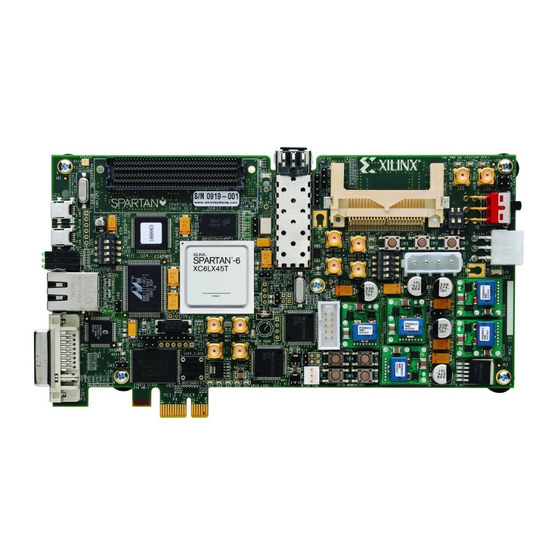
Page 7: Chapter 1: Sp605 Evaluation Board
Chapter 1 SP605 Evaluation Board Overview The SP605 board enables hardware and software developers to create or evaluate designs targeting the Spartan®-6 XC6SLX45T-3FGG484 FPGA. The SP605 provides board features common to many embedded processing systems. Some commonly used features include: a DDR3 component memory, a 1-lane PCI Express®... -
Page 8: Features
Chapter 1: SP605 Evaluation Board Features The SP605 board provides the following features: • 1. Spartan-6 XC6SLX45T-3FGG484 FPGA • 2. 128 MB DDR3 Component Memory • 3. SPI x4 Flash • 4. Linear BPI Flash • 5. System ACE CF and CompactFlash Connector •... -
Page 9: Block Diagram
AC Adapter and 12V Input Power Jack/Switch ♦ Onboard Power Regulation Block Diagram Figure 1-1 shows a high-level block diagram of the SP605 and its peripherals. X-Ref Target - Figure 1-1 1-Lane I/Fs: PCIe 125 MHz Clk Part of PCIe Edge Conn. -
Page 10: Related Xilinx Documents
Chapter 1: SP605 Evaluation Board Related Xilinx Documents Prior to using the SP605 Evaluation Board, users should be familiar with Xilinx resources. See the following locations for additional documentation on Xilinx tools and solutions: • ISE: www.xilinx.com/ise • Answer Browser: www.xilinx.com/support... - Page 11 Detailed Description Table 1-1: SP605 Features (Cont’d) Schematic Number Feature Notes Page Linear BPI Flash x16 Numonyx JS28F256P30T95 SystemACE CompactFlash XCCACE-TQ144I Controller Socket USB JTAG Conn. (USB Mini-B) USB JTAG Download Circuit 200 MHz OSC, oscillator socket, Clock Generation 13, 14 SMA connectors a.
-
Page 12: Spartan-6 Xc6Slx45T-3Fgg484 Fpga
21, 26 Controller b. Mini-Fit Type 6-Pin, ATX 12V input power connectors Type 4-pin 1. Spartan-6 XC6SLX45T-3FGG484 FPGA A Xilinx Spartan-6 XC6SLX45T-3FGG484 FPGA is installed on the Embedded Development Board. References See the Spartan-6 FPGA Data Sheet. [Ref 1] Configuration The SP605 supports configuration in the following modes: •... -
Page 13: I/O Voltage Rails
2. 128 MB DDR3 Component Memory There are 128 MB of DDR3 memory available on the SP605 board. A 1-Gb Micron MT41J64M16LA-187E (96-ball) DDR3 memory component is accessible through Bank 3 of the LX45T device. The Spartan-6 FPGA hard memory controller is used for data transfer across the DDR3 memory interface's 16-bit data path using SSTL15 signaling. - Page 14 Chapter 1: SP605 Evaluation Board Table 1-4: FPGA On-Chip (OCT) Termination External Resistor Requirements U1 FPGA Pin FPGA Pin Number Board Connection for OCT No Connect 100 ohms to GROUND Table 1-5 shows the connections and pin numbers for the DDR3 Component Memory.
- Page 15 UDQS_N MEM1_LDM MEM1_UDM MEM1_RESET_B RESET_B References See the Micron Technology, Inc. DDR3 SDRAM Specification for more information. [Ref 12] Also, see the Spartan-6 FPGA Memory Controller User Guide. [Ref 3] SP605 Hardware User Guide www.xilinx.com UG526 (v1.1.1) February 1, 2010...
-
Page 16: Spi X4 Flash
Chapter 1: SP605 Evaluation Board 3. SPI x4 Flash The Xilinx Spartan-6 FPGA hosts a SPI interface which is visible to the Xilinx iMPACT configuration tool. The SPI memory device operates at 3.0V; the Spartan-6 FPGA I/Os are 3.3V tolerant and provide electrically compatible logic levels to directly access the SPI flash through a 2.5V bank. - Page 17 1. Not a U1 FPGA pin References See the Winbond Serial Flash Memory Data Sheet for more information. [Ref 13] See the XPS Serial Peripheral Interface Data Sheet for more information. [Ref 4] SP605 Hardware User Guide www.xilinx.com UG526 (v1.1.1) February 1, 2010...
-
Page 18: Linear Bpi Flash
Chapter 1: SP605 Evaluation Board 4. Linear BPI Flash A Numonyx JS28F256P30 Linear Flash memory (U25) on the SP605 (Figure 1-5) provides 32 MB of non-volatile storage that can be used for configuration as well as software storage. The Linear Flash is operated in asynchronous mode. - Page 19 FLASH_D9 AB19 FLASH_D10 DQ10 AA18 FLASH_D11 DQ11 AB18 FLASH_D12 DQ12 FLASH_D13 DQ13 AA12 FLASH_D14 DQ14 AB12 FLASH_D15 DQ15 FMC_PWR_GOOD_FLASH_RST_B RST_B FLASH_WE_B WE_B FLASH_OE_B OE_B FLASH_CE_B CE_B FLASH_ADV_B ADV_B FLASH_WAIT WAIT SP605 Hardware User Guide www.xilinx.com UG526 (v1.1.1) February 1, 2010...
-
Page 20: Fpga Design Considerations For The Configuration Flash
Chapter 1: SP605 Evaluation Board FPGA Design Considerations for the Configuration Flash The SP605 has the P30 BPI flash connected to the FPGA dual use configuration pins and is not shared. It can be used to configure the FPGA, and then controlled post-configuration via the FPGA fabric. - Page 21 SYSACE_D0 MPD00 SYSACE_D1 MPD01 SYSACE_D2 MPD02 SYSACE_D3 MPD03 SYSACE_D4 MPD04 SYSACE_D5 MPD05 SYSACE_D6 MPD06 SYSACE_D7 MPD07 SYSACE_MPA00 MPA00 SYSACE_MPA01 MPA01 SYSACE_MPA02 MPA02 SYSACE_MPA03 MPA03 SYSACE_MPA04 MPA04 SYSACE_MPA05 MPA05 SYSACE_MPA06 MPA06 SP605 Hardware User Guide www.xilinx.com UG526 (v1.1.1) February 1, 2010...
-
Page 22: Usb Jtag
6. USB JTAG JTAG configuration is provided through onboard USB-to-JTAG configuration logic where a computer host accesses the SP605 JTAG chain through a Type-A (computer host side) to Type-Mini-B (SP605 side) USB cable. The JTAG chain of the board is illustrated in Figure 1-6. -
Page 23: Clock Generation
1-7. When the VITA 57.1 FMC LPC expansion connector is populated with an expansion module that has a JTAG chain, jumper J19 must be set to connect pins 2-3 in order to include the FMC expansion module's JTAG chain in the main SP605 JTAG chain. -
Page 24: Oscillator Socket (Single-Ended, 2.5V Or 3.3V)
Oscillator Socket (Single-Ended, 2.5V or 3.3V) One populated single-ended clock socket (X2) is provided for user applications. The option of 2.5V or 3.3V power may be selected via a 0 ohm resistor selection. The SP605 board is shipped with a 27 MHz 2.5V oscillator installed. -
Page 25: Sma Connectors (Differential)
One (1) MGT is wired to MGT SMA connectors (J36, J37) • One (1) MGT is wired to the SFP Module connector (P4) The SP605 includes a set of six SMA connectors for the GTP (MGT) RX/TX Port and GTP (MGT) Clock as described in Figure 1-10 Table 1-10. - Page 26 Chapter 1: SP605 Evaluation Board X-Ref Target - Figure 1-10 J35 32K10K-400E3 GND1 GND2 GND3 SMA_RX_C_N GND4 GND5 GND6 GND7 SMA_RX_N SMA_RX_P 32K10K-400E3 GND1 GND2 GND3 SMA_RX_C_P GND4 GND5 GND6 GND7 SMA MGT Connectors J33 32K10K-400E3 GND1 GND2 GND3 GND4...
- Page 27 Detailed Description Table 1-10: GTP SMA Clock Connections U1 FPGA Pin Schematic Net Name SMA Pin SMA_RX_N J35.1 SMA_RX_P J34.1 SMA_TX_N J33.1 SMA_TX_P J32.1 SMA_REFCLK_N J36.1 SMA_REFCLK_P J37.1 SP605 Hardware User Guide www.xilinx.com UG526 (v1.1.1) February 1, 2010...
-
Page 28: Pci Express Endpoint Connectivity
AC adapter might be required. If a different AC adapter is used, its load regulation should be better than ±10%. SP605 power slide switch SW2 turns the board on and off by controlling the 12V supply to the board. - Page 29 Also, see the following websites for more information about the Spartan-6 FPGA Integrated Endpoint Block for PCI Express: • Product information, http://www.xilinx.com/products/ipcenter/S6_PCI_Express_Block.htm • IP data sheets, http://www.xilinx.com/support/documentation/ipbusinterfacei- o_pci-express.htm#131486 In addition, see the PCI Express specifications for more information. [Ref 16] SP605 Hardware User Guide www.xilinx.com UG526 (v1.1.1) February 1, 2010...
-
Page 30: Sfp Module Connector
Chapter 1: SP605 Evaluation Board 10. SFP Module Connector The board contains a small form-factor pluggable (SFP) connector and cage assembly that accepts SFP modules. The SFP interface is connected to MGT Bank 123 on the FPGA. The SFP module serial ID interface is connected to the "SFP" IIC bus (see “14. -
Page 31: 100/1000 Tri-Speed Ethernet Phy
Detailed Description 11. 10/100/1000 Tri-Speed Ethernet PHY The SP605 uses the onboard Marvell Alaska PHY device (88E1111) for Ethernet communications at 10, 100, or 1000 Mb/s. The board supports a GMII interface from the FPGA to the PHY. The PHY connection to a user-provided Ethernet cable is through a Halo HFJ11-1G01E RJ-45 connector with built-in magnetics. - Page 32 Chapter 1: SP605 Evaluation Board Table 1-15: Ethernet PHY Connections (Cont’d) U46 M88E111 U1 FPGA Pin Schematic Net Name Pin Number Pin Name PHY_RXD7 RXD7 PHY_TXC_GTPCLK GTXCLK PHY_TXCLK TXCLK PHY_TXER TXER PHY_TXCTL_TXEN TXEN PHY_TXD0 TXD0 PHY_TXD1 TXD1 PHY_TXD2 TXD2 PHY_TXD3...
-
Page 33: Usb-To-Uart Bridge
The SP605 contains a Silicon Labs CP2103GM USB-to-UART bridge device (U4) which allows connection to a host computer with a USB cable. The USB cable is supplied in this evaluation kit (Type A end to host computer, Type Mini-B end to SP605 connector J23). Table 1-16 details the SP605 J23 pinout. -
Page 34: Dvi Codec
Chapter 1: SP605 Evaluation Board 13. DVI CODEC A DVI connector (P3) is present on the board to support an external video monitor. The DVI circuitry utilizes a Chrontel CH7301C (U31) capable of 1600 X 1200 resolution with 24- bit color. The video interface chip drives both the digital and analog signals to the DVI connector. -
Page 35: Iic Bus
Detailed Description 14. IIC Bus The SP605 implements three IIC bus interfaces at the FPGA. The MAIN IIC bus hosts four items: • FPGA U1 Bank 1 "MAIN" IIC interface • 8-Kb NV Memory U4 • FMC LPC connector J2 •... -
Page 36: 8-Kb Nv Memory
U31, Chrontel CH7301C 8-Kb NV Memory The SP605 hosts a 8-Kb ST Microelectronics M24C08-WDW6TP IIC parameter storage memory device (U4). The IIC address of U4 is 0b1010100, and U4 is not write protected (WP pin 7 is tied to GND). - Page 37 Not Applicable Tied to GND References See the ST Micro M24C08 Data Sheet for more information. [Ref 18] In addition, see the Xilinx XPS IIC Bus Interface Data Sheet. [Ref 8] SP605 Hardware User Guide www.xilinx.com UG526 (v1.1.1) February 1, 2010...
-
Page 38: Status Leds
Chapter 1: SP605 Evaluation Board 15. Status LEDs Table 1-21 defines the status LEDs. Table 1-21: Status LEDs Reference Signal Name Color Label Description Designator FMC_PWR_GOOD_FLASH_RST_B Green FMC PWR GD FMC Power Good FPGA_DONE Green DONE FPGA DONE GPIO_LED_0 Green... -
Page 39: Ethernet Phy Status Leds
The Ethernet PHY status LEDs (DS11-DS13) are mounted in right-angle plastic housings to make them visible on the connector end of the board when the SP605 board is installed into a PC motherboard. This cluster of six LEDs is installed adjacent to the RJ45 Ethernet jack... -
Page 40: Fpga Init And Done Leds
Chapter 1: SP605 Evaluation Board FPGA INIT and DONE LEDs The typical Xilinx FPGA power up and configuration status LEDs are present on the SP605. The red INIT LED DS17 comes on momentarily after the FPGA powers up and during its internal power-on process. -
Page 41: User I/O
Detailed Description 16. User I/O The SP605 provides the following user and general purpose I/O capabilities: • User LEDs • User Pushbutton Switches • User DIP Switch • User SIP Header • User SMA GPIO User LEDs The SP605 provides four active-High green LEDs as described in... -
Page 42: User Pushbutton Switches
Chapter 1: SP605 Evaluation Board User Pushbutton Switches The SP605 provides five active-High pushbutton switches: SW4, SW5, SW6, SW7 and SW8. The five pushbuttons all have the same topology as the sample shown in Figure 1-16. Four pushbuttons are assigned as GPIO, and the fifth is assigned as a CPU_RESET. -
Page 43: User Dip Switch
Detailed Description User DIP Switch The SP605 includes an active-High four-pole DIP switch, as described in Figure 1-17 Table 1-25. Three poles (switches 1-3) are pulled up to 2.5V, and one pole (switch 4) is pulled up to 1.5V, when closed. -
Page 44: User Sip Header
Chapter 1: SP605 Evaluation Board User SIP Header The SP605 includes a 6-pin single-inline (SIP) male pin header (J55) for FPGA GPIO access. Four pins of J55 are wired to the FPGA through 200 ohm series resistors and a level shifter, and the remaining two J55 pins are wired to 3.3V and GND. -
Page 45: User Sma Gpio
Detailed Description User SMA GPIO The SP605 includes an pair of SMA connectors for GPIO as described in Figure 1-19 Table 1-27. X-Ref Target - Figure 1-19 32K10K-400E3 GND1 GND2 GND3 GND4 GND5 GND6 GND7 USER_SMA_GPIO_N 32K10K-400E3 USER_SMA_GPIO_P GND1 GND2... -
Page 46: Switches
Mode DIP Switch SW1 (Active-High) Power On/Off Slide Switch SW2 SW2 is the SP605 board main power on/off switch. Sliding the switch actuator from the off to on position applies 12V power from either J18 (6-pin Mini-Fit) or J27 (4-pin ATX) power connector to the VCC12_P power plane. -
Page 47: Fpga_Prog_B Pushbutton Sw3 (Active-Low)
“5. System ACE CF and CompactFlash Connector,” page 20 for more details. X-Ref Target - Figure 1-22 Silkscreen: "SYSACE RESET" SYSACE_RESET_B Pushbutton UG526_22 _092409 Figure 1-22: System ACE CF RESET_B Pushbutton SW9 SP605 Hardware User Guide www.xilinx.com UG526 (v1.1.1) February 1, 2010... -
Page 48: System Ace Cf Compactflash Image Select Dip Switch S1 (Active-High)
Chapter 1: SP605 Evaluation Board System ACE CF CompactFlash Image Select DIP Switch S1 (Active-High) System ACE CF CompactFlash (CF) image select DIP switch S1, switches 1–3 (Figure 1-23) select which CF resident bitstream image is downloaded to the FPGA. S1 switches 1–3 offer eight binary addresses. -
Page 49: Mode Dip Switch Sw1 (Active-High)
Figure 1-24: FPGA Mode DIP Switch SW1 References For more information, refer to the Spartan-6 FPGA Configuration User Guide [Ref 2]. See Table 1-30, page 55 for the configuration modes. SP605 Hardware User Guide www.xilinx.com UG526 (v1.1.1) February 1, 2010... -
Page 50: Vita 57.1 Fmc Lpc Connector
2 differential clocks Note: The SP605 board VADJ voltage for the FMC LPC connector J2 is fixed at 2.5V (non- adjustable). The 2.5V rail cannot be turned off. The SP605 VITA 57.1 FMC interfaces are compatible with 2.5V mezzanine cards capable of supporting 2.5V VADJ. - Page 51 AB10 FMC_LA23_N IIC_SCL_MAIN FMC_LA26_P IIC_SDA_MAIN FMC_LA26_N FMC_CLK1_M2C_P FMC_PRSNT_M2C_L FMC_CLK1_M2C_N FMC_CLK0_M2C_P FMC_LA00_CC_P FMC_CLK0_M2C_N FMC_LA00_CC_N FMC_LA02_P FMC_LA03_P FMC_LA02_N FMC_LA03_N FMC_LA04_P FMC_LA08_P FMC_LA04_N FMC_LA08_N FMC_LA07_P FMC_LA12_P FMC_LA07_N FMC_LA12_N FMC_LA11_P FMC_LA16_P FMC_LA11_N FMC_LA16_N FMC_LA15_P SP605 Hardware User Guide www.xilinx.com UG526 (v1.1.1) February 1, 2010...
-
Page 52: Power Management
Mini-Fit type connector J18. The AC-to-DC power supply included in the kit has a mating 6-pin plug. When the SP605 is installed into a table top or tower PC's PCIe slot, the SP605 is typically powered from the PC ATX power supply. One of the PCs ATX hard disk type 4-pin power connectors is plugged into SP605 connector J27. -
Page 53: Onboard Power Regulation
Power Management Onboard Power Regulation Figure 1-25 shows the SP605 onboard power supply architecture. The SP605 uses Texas Instruments power controllers for primary core power control and monitoring. X-Ref Target - Figure 1-25 Power Supply Jack J18 or J27 Linear Regulator Op Amps 5.0V@1.5A max... - Page 54 Chapter 1: SP605 Evaluation Board Table 1-29: Onboard Power System Devices Reference Power Rail Net Power Rail Schematic Device Type Description Designator Name Voltage Page UCD9240PFC PMBus Controller - Core (Addr = 52) PTD08A010W 10A 0.6V - 3.6V Adj. Switching Regulator VCCINT_FPGA 1.20V...
-
Page 55: Configuration Options
4. Default setting due to internal pull-up termination on Mode pins. With the mode switch SW1 set to 01, the SP605 will attempt to boot or load a bitstream from either the SPI X4 Flash device U32 or a user supplied SPI Flash memory mezzanine... - Page 56 Chapter 1: SP605 Evaluation Board www.xilinx.com SP605 Hardware User Guide UG526 (v1.1.1) February 1, 2010...
- Page 57 Appendix A Default Jumper and Switch Settings Table A-1 shows the default switch settings and Table A-2, page 58 shows the default jumper settings for the SP605. Table A-1: Default Switch Settings REFDES Function/Type Default Board power slide-switch FPGA mode 2-pole DIP switch, Slave SelectMAP...
- Page 58 Jump 1-2 SFP Enabled Jump 1-2 SPI Memory Select SPI Select SPI X4 Memory U32 Jump 1-2 System ACE CF Error LED System ACE CF Error LED DS18 Enabled Jump 1-2 www.xilinx.com SP605 Hardware User Guide UG526 (v1.1.1) February 1, 2010...
- Page 59 12P0V G ND LA33_P 3P 3V LA32_P LA33_N 12P0V LA32_N 3P3V G ND G ND VADJ 3P3V V ADJ G ND 3P 3V UG526_26_092709 Figure B-1: FMC LPC Connector Pinout SP605 Hardware User Guide www.xilinx.com UG526 (v1.1.1) February 1, 2010...
- Page 60 Appendix B: VITA 57.1 FMC LPC Connector Pinout www.xilinx.com SP605 Hardware User Guide UG526 (v1.1.1) February 1, 2010...
-
Page 61: For More Information
Appendix C SP605 Master UCF The UCF template is provided for designs that target the SP605. Net names provided in the constraints below correlate with net names on the SP605 rev. C schematic. On identifying the appropriate pins, the net names below should be replaced with net names in the user RTL. - Page 62 Appendix C: SP605 Master UCF NET "FLASH_WE_B" LOC = "R20"; ## 14 on U25 NET "FLASH_OE_B" LOC = "P22"; ## 32 on U25 NET "FLASH_CE_B" LOC = "P21"; ## 30 on U25 NET "FLASH_ADV_B" LOC = "T19"; ## 46 on U25 ## NET "FMC_PWR_GOOD_FLASH_RST_B"...
- Page 63 ## C8 on U42 NET "MEM1_DQ14" LOC = "Y2"; ## B8 on U42 NET "MEM1_DQ15" LOC = "Y1"; ## A7 on U42 NET "MEM1_LDM" LOC = "N4"; ## E7 on U42 SP605 Hardware User Guide www.xilinx.com UG526 (v1.1.1) February 1, 2010...
- Page 64 Appendix C: SP605 Master UCF NET "MEM1_LDQS_N" LOC = "N1"; ## G3 on U42 NET "MEM1_LDQS_P" LOC = "N3"; ## F3 on U42 NET "MEM1_ODT" LOC = "L6"; ## K1 on U42 NET "MEM1_RAS_B" LOC = "M5"; ## J3 on U42 NET "MEM1_RESET_B"...
- Page 65 Pullup and pulldown resistors to a single point power or GND are included Series resistors are included DNP = do not populate, no component will be installed on the PCB at this location SP605 Hardware User Guide www.xilinx.com UG526 (v1.1.1) February 1, 2010...
- Page 66 Appendix C: SP605 Master UCF www.xilinx.com SP605 Hardware User Guide UG526 (v1.1.1) February 1, 2010...
- Page 67 This appendix provides references to documentation supporting Spartan-6 FPGAs, tools, and IP. For additional information, see www.xilinx.com/support/documentation/index.htm. Xilinx documents supporting the SP605 Evaluation Board: DS162, Spartan-6 FPGA Data Sheet: DC and Switching Characteristics UG380, Spartan-6 FPGA Configuration User Guide UG388, Spartan-6 FPGA Memory Controller User Guide...
Need help?
Do you have a question about the SP605 and is the answer not in the manual?
Questions and answers