
Related Manuals for Xilinx AC701


Summary of Contents for Xilinx AC701
- Page 1 AC701 Evaluation Board for the Artix-7 FPGA User Guide UG952 (v1.0) October 23, 2012...
-
Page 2: Revision History
Limited Warranties which can be viewed at http://www.xilinx.com/warranty.htm; IP cores may be subject to warranty and support terms contained in a license issued to you by Xilinx. Xilinx products are not designed or intended to be fail-safe or for use in any application requiring fail-safe performance;... -
Page 3: Table Of Contents
AC701 Board Features ........ - Page 4 ..............88 www.xilinx.com AC701 Evaluation Board UG952 (v1.0) October 23, 2012...
-
Page 5: Chapter 1: Ac701 Evaluation Board Features
Chapter 1 AC701 Evaluation Board Features Overview The AC701 evaluation board for the Artix™-7 FPGA provides a hardware environment for developing and evaluating designs targeting the Artix-7 XC7A200T-2FBG676C FPGA. The AC701 board provides features common to many embedded processing systems, including a DDR3 SODIMM memory, an 4-lane PCI Express®... - Page 6 • Quad SPI • USB JTAG configuration port • Platform cable header JTAG configuration port The AC701 board block diagram is shown in Figure 1-1. The AC701 board schematics are available for download from: www.xilinx.com AC701 Evaluation Board UG952 (v1.0) October 23, 2012...
-
Page 7: Feature Descriptions
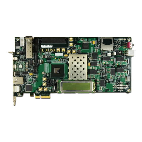
Feature Descriptions http://www.xilinx.com/AC701 Caution! The AC701 board can be damaged by electrostatic discharge (ESD). Follow standard ESD prevention measures when handling the board X-Ref Target - Figure 1-1 1 GB DDR3 Memory FMC Connector 10/100/1000 Ethernet (SODIMM) (HPC) Interface Differential Clock... - Page 8 Chapter 1: AC701 Evaluation Board Features X-Ref Target - Figure 1-2 Round callout references a component Square callout references a component on the front side of the board on the back side of the board UG952_c1_02_101512 Figure 1-2: AC701 Board Components...
-
Page 9: Artix-7 Fpga
For further information on Artix-7 FPGAs, see DS180 , 7 Series FPGAs Overview FPGA Configuration The AC701 board supports two of the five 7 Series FPGA configuration modes: • Master SPI using the on-board Quad SPI Flash memory • JTAG using a standard-A to micro-B USB cable for connecting the host PC to the... - Page 10 For full details on configuring the FPGA, see UG470, 7 Series FPGAs Configuration User Guide Encryption Key Backup Circuit FPGA U1 implements bitstream encryption key technology. The AC701 board provides the encryption key backup battery circuit shown in Figure 1-4. The rechargeable 1.5V lithium button-type battery B1 is soldered to the board with the positive output connected to FPGA U1 VCCBATT pin G14.
- Page 11 Figure 1-4: Encryption Key Backup Circuit I/O Voltage Rails In addition to Bank 0, there are 8 I/O banks available on the Artix-7 device. The voltages applied to the FPGA I/O banks used by the AC701 board are listed in Table 1-3.
-
Page 12: Ddr3 Memory Module
Chapter 1: AC701 Evaluation Board Features DDR3 Memory Module [Figure 1-2, callout 2] The memory module at J1 is a 1 GB DDR3 small outline dual-inline memory module (SODIMM). It provides volatile synchronous dynamic random access memory (SDRAM) for storing user code and data. The SODIMM socket has a perforated EMI shield... - Page 13 DQ17 DDR3_D18 DQ18 DDR3_D19 DQ19 DDR3_D20 DQ20 DDR3_D21 DQ21 DDR3_D22 DQ22 DDR3_D23 DQ23 DDR3_D24 DQ24 DDR3_D25 DQ25 DDR3_D26 DQ26 DDR3_D27 DQ27 DDR3_D28 DQ28 DDR3_D29 DQ29 DDR3_D30 DQ30 DDR3_D31 DQ31 DDR3_D32 DQ32 AC701 Evaluation Board www.xilinx.com UG952 (v1.0) October 23, 2012...
- Page 14 Chapter 1: AC701 Evaluation Board Features Table 1-4: DDR3 Memory Connections to the FPGA (Cont’d) J1 DDR3 Memory U1 FPGA Pin Net Name Pin Number Pin Name DDR3_D33 DQ33 DDR3_D34 DQ34 DDR3_D35 DQ35 DDR3_D36 DQ36 DDR3_D37 DQ37 DDR3_D38 DQ38 DDR3_D39...
- Page 15 DDR3_DQS4_P DQS4_P DDR3_DQS5_N DQS5_N DDR3_DQS5_P DQS5_P DDR3_DQS6_N DQS6_N DDR3_DQS6_P DQS6_P DDR3_DQS7_N DQS7_N DDR3_DQS7_P DQS7_P DDR3_ODT0 ODT0 DDR3_ODT1 ODT1 DDR3_RESET_B RESET_B DDR3_S0_B S0_B DDR3_S1_B S1_B DDR3_TEMP_ EVENT_B EVENT DDR3_WE_B WE_B DDR3_CAS_B CAS_B AC701 Evaluation Board www.xilinx.com UG952 (v1.0) October 23, 2012...
-
Page 16: Quad-Spi Flash Memory
The configuration section of UG470, 7 Series FPGAs Configuration User Guide provides details on using the Quad-SPI Flash memory. Figure 1-5 shows the connections of the Quad-SPI Flash memory on the AC701 board. For more details, see the Numonyx N25Q256A13ESF40G data sheet http://www.micron.com. www.xilinx.com AC701 Evaluation Board... -
Page 17: Spi External Programming Header
Table 1-6: SPI J7 Connections to the FPGA Schematic Net U1 FPGA Pin J7 Pin Name AE16 FPGA_PROG_B FLASH_D3 FLASH_D2 J3.2 QSPI_CS_B FLASH_D0 FLASH_D1 FPGA_CCLK VCC3V3 Figure 1-6 shows the J7 SPI external programming connector. AC701 Evaluation Board www.xilinx.com UG952 (v1.0) October 23, 2012... -
Page 18: Sd Card Interface
[Figure 1-2, callout 4] The AC701 board includes a secure digital input/output (SDIO) interface to provide user-logic access to general purpose non-volatile SDIO memory cards and peripherals. The SD card slot is designed to support 50 MHz high speed SD cards. - Page 19 Table 1-7: SDIO Connections to the FPGA U29 SDIO Connector U1 FPGA Pin Schematic Net Name Name Pin Number Pin Name SDIO_SDWP SDWP SDIO_SDDET SDDET SDIO_CMD SDIO_CLK SDIO_DAT2 DAT2 SDIO_DAT1 DAT1 SDIO_DAT0 DAT0 SDIO_CD_DAT3 CD_DAT3 AC701 Evaluation Board www.xilinx.com UG952 (v1.0) October 23, 2012...
-
Page 20: Usb Jtag Module
UG952_c1_08_100212 Figure 1-8: JTAG Chain Block Diagram When an FMC daughter card is attached to the AC701 board it is automatically added to the JTAG chain through electronically controlled single-pole single-throw (SPST) switches U27. The SPST switch is in a normally closed state and transitions to an open state when an FMC daughter card is attached. -
Page 21: Clock Generation
FPGA_TDI_BUF FPGA_TCK_BUF FPGA_TMS_BUF FPGA_TDO UG952_c1_09_101512 Figure 1-9: JTAG Circuit Clock Generation There are three clock sources available for the FPGA fabric on the AC701 board (refer to Table 1-8). Table 1-8: AC701 Board Clock Sources Clock Name Reference Description System Clock SiT9102 2.5V LVDS 200 MHz Fixed Frequency... - Page 22 [Figure 1-2, callout 6] The AC701 board has a 2.5V LVDS differential 200 MHz oscillator (U51) soldered onto the back side of the board and wired to an FPGA MRCC clock input on bank 34. This 200 MHz signal pair is named SYSCLK_P and SYSCLK_N, which are connected to FPGA U1 pins R3 and P3 respectively.
- Page 23 156.250 MHz. User applications can change the output frequency within the range of 10 MHz to 810 MHz through an I C interface. Power cycling the AC701 board will revert the user clock to its default frequency of 156.250 MHz. •...
- Page 24 Chapter 1: AC701 Evaluation Board Features User SMA Clock Input [Figure 1-2, callout 8] An external high-precision clock signal can be provided to the FPGA bank 15 by connecting differential clock signals through the onboard 50Ω SMA connectors J31 (P) and J32 (N).
- Page 25 Feature Descriptions GTP Clock MUX The AC701 board FPGA U1 MGT Bank 213 has two clock inputs, MGTREFCLK0 and MGTREFCLK1. Each clock input is driven by a capacitively-coupled clock sourced from a SY9544UMG 4-to-1 MUX. Each MUX has a clock source at three of its four inputs, the fourth input is not connected.
- Page 26 [Figure 1-2, callout 9] The AC701 board includes a pair of SMA connectors for a GTP clock that are wired to GTP quad bank 213 via clock MUX U4. This differential clock has signal names SMA_MGT_REFCLK_P and SMA_REFCLK_N, which are connected to MGT clock MUX U4 input 0 pins 4 and 2 respectively.
- Page 27 [Figure 1-2, callout 10] The AC701 board includes a Silicon Labs Si5324 jitter attenuator U24 on the back side of the board. FPGA user logic can implement a clock recovery circuit and then output this clock to a differential I/O pair on I/O bank 16 (REC_CLOCK_C_P, FPGA U1 pin D23 and REC_CLOCK_C_N, FPGA U1 pin D24) for jitter attenuation.
- Page 28 Chapter 1: AC701 Evaluation Board Features FMC HPC GBT Clocks The FMC HPC connector J30 sources two MGT clocks, FMC1_HPC_GBTCLK0_M2C_P/N from connector section D, and FMC1_HPC_GBTCLK1_M2C_P/N from connector section B. Table 1-10 Table 1-11 list the MGT clock connections. Table 1-10: MUX U3 SY89544UMG MGT Clock Inputs...
- Page 29 SEL0 PWRPAD SEL1 MGT_CLK0_SEL1 MGT_CLK0_SEL0 VCC2V5 R454 1/10W NDS336P SFP_MGT_CLK_SEL0 460 mW R332 1/10W VCC2V5 R455 1/10W NDS336P SFP_MGT_CLK_SEL1 460 mW R333 1/10W UG952_c1_16_101612 Figure 1-16: MGT Clock MUX U3 Circuit AC701 Evaluation Board www.xilinx.com UG952 (v1.0) October 23, 2012...
- Page 30 Chapter 1: AC701 Evaluation Board Features X-Ref Target - Figure 1-17 VCC2V5 VCC2V5 SY89544UMG C106 0.1μF VCC1 VCC3 VCC2 VCC4 SMA_MGT_REFCLK_P VCC5 VCC6 C321 SMA_MGT_REFCLK_N VCC7 0.1μF SI5324_OUT1_C_P VCC8 SFP_MGT_CLK1_P SI5324_OUT1_C_N SFP_MGT_CLK1_P FMC1_HBC_GBTCLK1_M2C_C_P C322 GND1 TO MGT BANK 213 0.1μF...
-
Page 31: Gtp Transceivers
The GTP transceivers in 7 series FPGAs are grouped into four channels described as Quads. The reference clock for a Quad can be sourced from the Quad above or Quad below the GTP Quad of interest. There are two GTP Quads on the AC701 board with connectivity as shown here: •... - Page 32 Chapter 1: AC701 Evaluation Board Features Table 1-12: GTP Interface Connections for FPGA U1 Connected Transceiver Bank Placement Pin Name Schematic Net Name Connected Device Number GTP_BANK_213 GTPE2_CHANNEL_ AC10 MGTPTXP0_213 SFP_TX_P P3.18 SFP+ Conn. P3 X0Y0 AD10 MGTPTXN0_213 SFP_TX_N P3.19 SFP+ Conn.
-
Page 33: Pci Express Edge Connector
100Ω differential pair. The 7 series FPGAs GTP transceivers are used for multi-gigabit per second serial interfaces. The XC7A200T-2FBG676C FPGA (-2 speed grade) included with the AC701 board supports up to Gen2 x4. The PCIe clock is input from the edge connector. It is AC coupled to the FPGA through the MGTREFCLK0 pins of Quad 216. -
Page 34: Sfp/Sfp+ Connector
7 Series FPGAs Integrated Block for PCI Express User Guide (AXI). SFP/SFP+ Connector [Figure 1-2, callout 13] The AC701 board contains a small form-factor pluggable (SFP+) connector and cage assembly that accepts SFP or SFP+ modules. Figure 1-20 shows the SFP+ module connector circuitry. - Page 35 Table 1-13: FPGA U1 to SFP+ Module Connections FPGA Pin Schematic SFP+ Pin SFP+ Pin Name (U1) Net Name (P5) (P5) AD12 SFP_RX_N RD_N AC12 SFP_RX_P RD_P AD10 SFP_TX_N TX_N AC10 SFP_TX_P TX_P SFP_TX_DISABLE TX_DISABLE SFP_LOS AC701 Evaluation Board www.xilinx.com UG952 (v1.0) October 23, 2012...
-
Page 36: 10/100/1000 Mb/S Tri-Speed Ethernet Phy
[Figure 1-2, callout 14] The AC701 board uses the Marvell Alaska PHY device (88E1116R) at U12 for Ethernet communications at 10 Mb/s, 100 Mb/s, or 1,000 Mb/s. The board supports RGMII mode only. The PHY connection to a user-provided ethernet cable is through a Halo HFJ11-1G01E RJ-45 connector (P4) with built-in magnetics. - Page 37 Schematic Net Name Name PHY_MDIO MDIO PHY_MDC PHY_TX_CLK TX_CLK PHY_TX_CTRL TX_CTRL PHY_TXD3 TXD3 PHY_TXD2 TXD2 PHY_TXD1 TXD1 PHY_TXD0 TXD0 PHY_RX_CLK RX_CLK PHY_RX_CTRL RX_CTRL PHY_RXD3 RXD3 PHY_RXD2 RXD2 PHY_RXD1 RXD1 PHY_RXD0 RXD0 PHY_RESET_B RESET_B AC701 Evaluation Board www.xilinx.com UG952 (v1.0) October 23, 2012...
-
Page 38: Ethernet Phy User Leds
Chapter 1: AC701 Evaluation Board Features Ethernet PHY Clock Source A 25.00 MHz, 50 ppm crystal at X1 is the clock source for the 88E1116R PHY at U12. Figure 1-21 shows the clock source. X-Ref Target - Figure 1-21 C406 18pF 50V 25.00 MHz... -
Page 39: Usb-To-Uart Bridge
USB cable is plugged into the USB port on the AC701 board. Xilinx UART IP is expected to be implemented in the FPGA fabric. The FPGA supports the USB-to-UART bridge using four signal pins: Transmit (TX), Receive (RX), Request to Send (RTS), and Clear to Send (CTS). -
Page 40: Hdmi Video Output
[Figure 1-2, callout 17] The AC701 board provides a High-Definition Multimedia Interface (HDMI) video output using the Analog Devices ADV7511KSTZ-P HDMI transmitter (U48). The HDMI output is provided on a Molex 500254-1927 HDMI type-A connector (P2). The ADV7511 is wired to support 1080P 60Hz, YCbCr 4:4:4 encoding via 24-bit input data mapping. - Page 41 HDMI_CEC DSD3 DSD4 DSD5 DSD_CLK MCLK GND1 GND2 GND3 I2S0 GND4 I2S1 GND5 I2S2 GND6 I2S3 GND7 SCLK GND8 LRCLK GND9 GND10 R_EXT GND11 R102 UG952_c1_23_100312 Figure 1-23: HDMI Codec Circuit AC701 Evaluation Board www.xilinx.com UG952 (v1.0) October 23, 2012...
- Page 42 Chapter 1: AC701 Evaluation Board Features Table 1-19 lists the connections between the codec and the FPGA. Table 1-19: FPGA to HDMI Codec Connections (ADV7511) ADV7511 (U48) FPGA Pin (U1) Schematic Net Name Name AA24 HDMI_R_D4 HDMI_R_D5 HDMI_R_D6 HDMI_R_D7 HDMI_R_D8...
-
Page 43: Lcd Character Display
Information about the ADV7511 is available on the Analog Devices website at http://www.analog.com/en/index.html. LCD Character Display [Figure 1-2, callout 18] A 2-line by 16-character display is provided on the AC701 board (Figure 1-24). X-Ref Target - Figure 1-24 LCD Display (16 x 2) - Page 44 UG952_c1_25_100312 Figure 1-25: LCD Interface Circuit The AC701 board base board uses a male Samtec MTLW-107-07-G-D-265 2x7 header (J23) with 0.025-inch square posts on 0.100-inch centers for connecting to a Samtec SLW-107-01-L-D female socket on the LCD display panel assembly. The LCD header...
-
Page 45: I 2 C Bus Switch
C Bus Switch [Figure 1-2, callout 19] The AC701 board implements a single I C port on the FPGA (IIC_SDA_MAIN, IIC_SDA_SCL), which is routed through a Texas Instruments PCA9548 1-to-8 channel I switch (U49). The I C switch can operate at speeds up to 400 kHz. -
Page 46: Ac701 Board Leds
0b1010000, 0b0011000 SI5324_SDA/SCL 0b1010000 Information about the PCA9548 is available on the TI Semiconductor website at http://www.ti.com. AC701 Board LEDs Table 1-23 lists all LEDs on the AC701 board. Table 1-23: AC701 Board LEDs Reference Schematic Description Notes Designator Page... -
Page 47: User I/O
Notes: 1. The Lumex SML-LX0603GW LED is Green User I/O [Figure 1-2, callout - 25] The AC701 board provides the following user and general purpose I/O capabilities: • Four user LEDs (callout 21) • GPIO_LED_[3-0]: DS5, DS4, DS3, DS2 •... - Page 48 Chapter 1: AC701 Evaluation Board Features User GPIO LEDs [Figure 1-2, callout 21] Figure 1-28 shows the user LED circuits. X-Ref Target - Figure 1-28 GPIO_LED_0 GPIO_LED_1 GPIO_LED_2 GPIO_LED_3 R150 R149 R148 R147 49.9Ω 49.9Ω 49.9Ω 49.9Ω UG952_c1_28_100312 Figure 1-28: User LEDs www.xilinx.com...
- Page 49 FPGA_1V5 GPIO SW W GPIO SW C GPIO SW E 4.7kΩ 4.7kΩ 4.7kΩ 0.1 W 0.1 W 0.1 W FPGA_1V5 GPIO SW S 4.7kΩ 0.1 W UG952_c1_29_100312 Figure 1-29: User Pushbuttons AC701 Evaluation Board www.xilinx.com UG952 (v1.0) October 23, 2012...
- Page 50 Chapter 1: AC701 Evaluation Board Features GPIO DIP Switch [Figure 1-2, callout 23] Figure 1-30 shows the GPIO DIP Switch circuit. X-Ref Target - Figure 1-30 FPGA_1V5 GPIO_DIP_SW0 GPIO_DIP_SW1 GPIO_DIP_SW2 GPIO_DIP_SW3 SDA04H1SBD 4.7kΩ 4.7kΩ 0.1 W 0.1 W 4.7kΩ 4.7kΩ...
- Page 51 4-Pole DIP Switch (Active High) GPIO_DIP_SW0 SW2.1 GPIO_DIP_SW1 SW2.2 GPIO_DIP_SW2 SW2.3 GPIO_DIP_SW3 SW2.4 Rotary Encoder Switch (Active High) ROTARY_INCB SW10.6 ROTARY_PUSH SW10.5 ROTARY_INCA SW10.1 User SMA Connectors USER_SMA_GPIO_P J33.1 USER_SMA_GPIO_N J34.1 AC701 Evaluation Board www.xilinx.com UG952 (v1.0) October 23, 2012...
-
Page 52: Switches
[Figure 1-2, callout 26] The AC701 board power switch is SW15. Sliding the switch actuator from the Off to On position applies 12V power from J49, a 6-pin mini-fit connector. Green LED DS22 illuminates when the AC701 board power is on. See... - Page 53 J49, power switch SW15 and indicator LED DS22. X-Ref Target - Figure 1-33 VCC12 P SW15 VCC12 P IN R369 1kΩ C539 DS22 330μF PCIe Power UG952_c1_33_101612 Figure 1-33: Power On/Off Switch SW15 AC701 Evaluation Board www.xilinx.com UG952 (v1.0) October 23, 2012...
- Page 54 1-25. The mode switches M2, M1, and M0 are on SW1 positions 1, 2, and 3 respectively as shown in Figure 1-36. Note: On the AC701 Rev A and Rev B boards, SW1 switch position 2 is disabled and is not used. www.xilinx.com AC701 Evaluation Board UG952 (v1.0) October 23, 2012...
-
Page 55: Fpga Mezzanine Card Interface
[Figure 1-2, callout 29] The AC701 board supports the VITA 57.1 FPGA Mezzanine Card (FMC) specification by providing high pin count (HPC) connector J30. HPC J30 is keyed so that a the mezzanine card faces away from the AC701 board when connected. - Page 56 2 differential clocks • 159 ground and 15 power connections Note: The AC701 board VADJ voltage for HPC connector J30 is determined by the FMC VADJ power sequencing logic described in Power Management, page Table 1-26: HPC Connections, J30 to FPGA U1...
- Page 57 FMC1_HPC_LA27_N FMC1_HPC_LA23_P FMC1_HPC_IIC_SCL U52.19 FMC1_HPC_LA23_N FMC1_HPC_IIC_SDA U52.20 FMC1_HPC_LA26_P FMC1_HPC_LA26_N VCC12_P FMC1_HPC_TCK_BUF U19.13 VCC12_P FMC1_TDI_BUF U19.17 VCC3V3 FMC1_TDO_FPGA_TDI U19.2 VCC3V3 FMC1_HPC_TMS_BUF U19.15 VCC3V3 VCC3V3 VCC3V3 FMC1_HPC_HA01_CC_P AB21 FMC1_HPC_PG_M2C FMC1_HPC_HA01_CC_N AC21 FMC1_HPC_HA00_CC_P AA19 AC701 Evaluation Board www.xilinx.com UG952 (v1.0) October 23, 2012...
- Page 58 Chapter 1: AC701 Evaluation Board Features Table 1-26: HPC Connections, J30 to FPGA U1 (Cont’d) J30 FMC U1 FPGA J30 FMC U1 FPGA Schematic Net Name Schematic Net Name HPC Pin HPC Pin FMC1_HPC_HA05_P AD25 FMC1_HPC_HA00_CC_N AB19 FMC1_HPC_HA05_N AD26 FMC1_HPC_HA04_P...
- Page 59 FMC1_HPC_HA07_N AD24 FMC1_HPC_HA06_P AE23 FMC1_HPC_HA11_P AD20 FMC1_HPC_HA06_N AF23 FMC1_HPC_HA11_N AE20 FMC1_HPC_HA10_P AE22 FMC1_HPC_HA14_P AE18 FMC1_HPC_HA10_N AF22 FMC1_HPC_HA14_N AF18 FMC1_HPC_HA17_CC_P AA20 FMC1_HPC_HA18_P AA17 FMC1_HPC_HA17_CC_N AB20 FMC1_HPC_HA18_N AB17 FMC1_HPC_HA21_P AB16 FMC1_HPC_HA22_P FMC1_HPC_HA21_N AC16 AC701 Evaluation Board www.xilinx.com UG952 (v1.0) October 23, 2012...
-
Page 60: Power Management
[Figure 1-2, callout 30] The AC701 board uses power regulators and PMBus compliant system controllers from Texas Instruments to supply core and auxiliary voltages. The Texas Instruments Fusion Digital Power graphical user interface is used to monitor the voltage and current levels of the board power modules. - Page 61 1.7V–2.0V at 300 mA 1.5V/2=0.75V REFIN VTTDDR Source/Sink Regulator 3.3V POWER 0.75V at 3A 1.5V/2=0.75V REFIN DDR3_VTERM Switching Regulator 3.3V POWER 0.75V at 3A UG952_c1_37_100512 Figure 1-37: AC701 Board Onboard Power Regulators AC701 Evaluation Board www.xilinx.com UG952 (v1.0) October 23, 2012...
- Page 62 Chapter 1: AC701 Evaluation Board Features The AC701 board core and auxiliary voltages are listed in Table 1-25. Table 1-27: AC701 Board Onboard Power System Devices Reference Power Rail Net Power Rail Schematic Device Type Description Designator Name Voltage Page...
- Page 63 A jumper installed at J8 is the default setting. If a jumper is not installed on J8 at power-on, the signal FMC_VADJ_ON_B is high and the AC701 board will not energize the VCCO_VADJ 2.5V power. Installing a jumper at J8 after the AC701 board powers up in this mode will turn on the VCCO_VADJ rail. AC701 Evaluation Board www.xilinx.com...
- Page 64 VCCO_VADJ rail to be set to 1.8V or 3.3V instead of the default setting of 2.5V. Refer to AC701 board schematic page 46 for a brief discussion concerning selectable VCCO_VADJ voltages. The important controller-to-regulator circuit signals are VCCO_VADJ_EN and FMC_ADJ_SEL[1:0].
-
Page 65: Xadc Header
12-bit, 1 MSPS Analog-to-Digital Convertor (ADC) and on-chip sensors. See UG480, 7 Series FPGAs XADC Dual 12-Bit 1MSPS Analog-to-Digital Converter User Guide for details on the capabilities of the analog front end. Figure 1-39 shows the AC701 board XADC support features. AC701 Evaluation Board www.xilinx.com... - Page 66 UG952_c1_39_101612 Figure 1-39: Header XADC_VREF Voltage Source Options The AC701 board supports both the internal FPGA sensor measurements and the external measurement capabilities of the XADC. Internal measurements of the die temperature, VCCINT, VCCAUX, and VCCBRAM are available. The AC701 board VCCINT and VCCBRAM are provided by a common 1.0 V supply.
- Page 67 Digital IO. These pins should come from the same bank. These IOs should not XADC_GPIO_3, 2, 1, 0 19, 20, 17, 18 be shared with other functions because they are required to support three-state operation. AC701 Evaluation Board www.xilinx.com UG952 (v1.0) October 23, 2012...
-
Page 68: Configuration Options
Chapter 1: AC701 Evaluation Board Features Configuration Options The FPGA on the AC701 board can be configured using these methods: • Master SPI (uses the Quad-SPI Flash U7). • JTAG (uses the U26 Digilent USB-to-JTAG Bridge or J4 Download Cable connector). - Page 69 4.7K VCC3V3 R396 CCLK 261Ω DONE DS10 D[3:0] GREEN Bank 14 FCS_B N25Q256A13ESF40G QUAD SPI DQ[1:0] DQ2_WP DQ3_HOLD_B Oscillator EMCCLK 90 MHz SIT8103 UG952_c1_42_101612 Figure 1-42: AC701 Board QSPI Configuration Circuit AC701 Evaluation Board www.xilinx.com UG952 (v1.0) October 23, 2012...
- Page 70 Chapter 1: AC701 Evaluation Board Features www.xilinx.com AC701 Evaluation Board UG952 (v1.0) October 23, 2012...
-
Page 71: Appendix A: Default Switch And Jumper Settings
X-Ref Target - Figure A-1 ON Position = 1 2 3 4 OFF Position = 0 UG952_aA_01_100712 Figure A-1: SW2 Default Settings Table A-1: SW2 Default Switch Settings Position Function Default GPIO_DIP_SW0 GPIO_DIP_SW1 GPIO_DIP_SW2 GPIO_DIP_SW3 AC701 Evaluation Board www.xilinx.com UG952 (v1.0) October 23, 2012... -
Page 72: Configuration Dip Switch Sw1
Figure A-2: SW1 Default Settings The default mode setting M[2:0] = 001 selects Master SPI configuration at board power-on. Table A-2: SW1 Default Switch Settings Position Function Default FPGA_M2 FPGA_M1 FPGA_M0 www.xilinx.com AC701 Evaluation Board UG952 (v1.0) October 23, 2012... -
Page 73: Default Jumper Settings
Default Jumper Settings Default Jumper Settings The AC701 board default jumper configurations are listed in Table A-3. Table A-3: AC701 Default Jumper Settings Schematic Header Jumper Description Page 2-pin XADC VCCINT 4A range XADC_VCC5V0 = 5V REF3012 XADC_AGND L3 bypassed... - Page 74 Appendix A: Default Switch and Jumper Settings www.xilinx.com AC701 Evaluation Board UG952 (v1.0) October 23, 2012...
-
Page 75: Appendix B: Vita 57.1 Fmc Connector Pinouts
Figure B-1 shows the pinout of the FPGA mezzanine card (FMC) high pin count (HPC) connector defined by the VITA 57.1 FMC specification. For a description of how the AC701 board implements the FMC specification, see FPGA Mezzanine Card Interface, page 55... - Page 76 Appendix B: VITA 57.1 FMC Connector Pinouts www.xilinx.com AC701 Evaluation Board UG952 (v1.0) October 23, 2012...
-
Page 77: Appendix C: Master Ucf Listing
Master UCF Listing TheAC701 board master user constraints file (UCF) template provides for designs targeting the AC701 board. Net names in the constraints listed below correlate with net names on the latest AC701 board schematic. Users must identify the appropriate pins and replace the net names below with net names in the user RTL. - Page 78 14 VCCO - FPGA_3V3 - IO_L9P_T1_DQS_14 LCD_DB4_LS LOC = L25 | IOSTANDARD=LVCMOS33; # Bank 14 VCCO - FPGA_3V3 - IO_L9N_T1_DQS_D13_14 LCD_DB5_LS LOC = M24 | IOSTANDARD=LVCMOS33; # Bank 14 VCCO - FPGA_3V3 - IO_L10P_T1_D14_14 www.xilinx.com AC701 Evaluation Board UG952 (v1.0) October 23, 2012...
- Page 79 AC701 Board UCF Listing LCD_DB6_LS LOC = M25 | IOSTANDARD=LVCMOS33; # Bank 14 VCCO - FPGA_3V3 - IO_L10N_T1_D15_14 LCD_DB7_LS LOC = L22 | IOSTANDARD=LVCMOS33; # Bank 14 VCCO - FPGA_3V3 - IO_L11P_T1_SRCC_14 LCD_RS_LS LOC = L23 | IOSTANDARD=LVCMOS33; # Bank...
- Page 80 33 VCCO - FPGA_1V5 - IO_L15P_T2_DQS_33 DDR3_DQS1_N LOC = AE5 | IOSTANDARD=SSTL15; # Bank 33 VCCO - FPGA_1V5 - IO_L15N_T2_DQS_33 DDR3_D11 LOC = AE3 | IOSTANDARD=SSTL15; # Bank 33 VCCO - FPGA_1V5 - IO_L16P_T2_33 www.xilinx.com AC701 Evaluation Board UG952 (v1.0) October 23, 2012...
- Page 81 AC701 Board UCF Listing DDR3_D10 LOC = AF3 | IOSTANDARD=SSTL15; # Bank 33 VCCO - FPGA_1V5 - IO_L16N_T2_33 DDR3_D9 LOC = AF5 | IOSTANDARD=SSTL15; # Bank 33 VCCO - FPGA_1V5 - IO_L17P_T2_33 DDR3_D8 LOC = AF4 | IOSTANDARD=SSTL15; # Bank...
- Page 82 ; # Bank 216 - MGTRREF_216 #NET No Connect LOC = F13 | IOSTANDARD=LVDS_25 ; # Bank 216 - MGTREFCLK1P_216 #NET No Connect LOC = E13 | IOSTANDARD=LVDS_25 ; # Bank 216 - MGTREFCLK1N_216 www.xilinx.com AC701 Evaluation Board UG952 (v1.0) October 23, 2012...
-
Page 83: Appendix D: Board Setup
Figure D-1: Plug the 6-pin 2 x 3 Molex connector on the adapter cable into J49 on the AC701 board. b. Plug the 4-pin 1 x 4 peripheral power connector from the ATX power supply into the 4-pin adapter cable connector. - Page 84 Appendix D: Board Setup Slide the AC701 board power switch SW15 to the ON position. The PC can now be powered on. www.xilinx.com AC701 Evaluation Board UG952 (v1.0) October 23, 2012...
- Page 85 Board Specifications Dimensions Height 5.5 in (14.0 cm) Length 10.5 in (26.7 cm) Note: The AC701 board height exceeds the standard 4.376 in (11.15 cm) height of a PCI Express card. Environmental Temperature Operating: 0°C to +45°C Storage: –25°C to +60°C...
- Page 86 Appendix E: Board Specifications www.xilinx.com AC701 Evaluation Board UG952 (v1.0) October 23, 2012...
- Page 87 Topics include design assistance, advisories, and troubleshooting tips: http://www.xilinx.com/support/solcenters.htm Further Resources The most up to date information related to the AC701 board and its documentation is available on the following websites. The AC701 Artix-7 FPGA evaluation board Kit product page: http://www.xilinx.com/AC701 The AC701 Artix-7 FPGA evaluation board Kit Master Answer Record: http://www.xilinx.com/support/answers/518900.htm...
- Page 88 UG480, 7 Series FPGAs XADC Dual 12-Bit 1MSPS Analog-to-Digital Converter User Guide XTP230, AC701 Si570 Programming XTP229, AC701 Si570 Fixed Frequencies References Documents associated with other devices used by the AC701 board are available at these vendor websites: Analog Devices: http://www.analog.com/en/index.html...
Need help?
Do you have a question about the AC701 and is the answer not in the manual?
Questions and answers