Table of Contents
Advertisement
Artix-7 FPGA
AC701 Evaluation Kit
(Vivado Design Suite
2013.3)
Getting Started Guide
UG967 (v4.0.1) March 05, 2014
This document applies to the following software versions: Vivado Design Suite 2013.3 and 2013.4
This document applies to the following software versions: Vivado Design Suite 2013.3 and 2013.4
This document applies to the following software versions: Vivado Design Suite 2013.3 and 2013.4
This document applies to the following software versions: Vivado Design Suite 2013.3 and 2013.4
0402936-03
Advertisement
Table of Contents

Related Manuals for Xilinx Artix-7 FPGA AC701


Summary of Contents for Xilinx Artix-7 FPGA AC701
- Page 1 Artix-7 FPGA AC701 Evaluation Kit (Vivado Design Suite 2013.3) Getting Started Guide UG967 (v4.0.1) March 05, 2014 This document applies to the following software versions: Vivado Design Suite 2013.3 and 2013.4 This document applies to the following software versions: Vivado Design Suite 2013.3 and 2013.4 This document applies to the following software versions: Vivado Design Suite 2013.3 and 2013.4 This document applies to the following software versions: Vivado Design Suite 2013.3 and 2013.4 0402936-03...
- Page 2 (including loss of data, profits, goodwill, or any type of loss or damage suffered as a result of any action brought by a third party) even if such damage or loss was reasonably foreseeable or Xilinx had been advised of the possibility of the same.
-
Page 3: Revision History
Revision History The following table shows the revision history for this document. Date Version Revision 01/10/2013 Initial Xilinx release. 04/17/2013 Updated for Vivado® Design Suite 2013.1. Updated Introduction, Basic Hardware Bring-up with Built-In Self-Test, AMS Bring-up with the AMS101 Evaluation... - Page 4 AC701 Getting Started Guide www.xilinx.com UG967 (v4.0.1) March 05, 2014...
-
Page 5: Table Of Contents
............. 3 Getting Started with the Artix-7 FPGA AC701 Evaluation Kit Introduction . - Page 6 AC701 Getting Started Guide Send Feedback UG967 (v4.0.1) March 05, 2014...
-
Page 7: Getting Started With The Artix-7 Fpga Ac701 Evaluation Kit
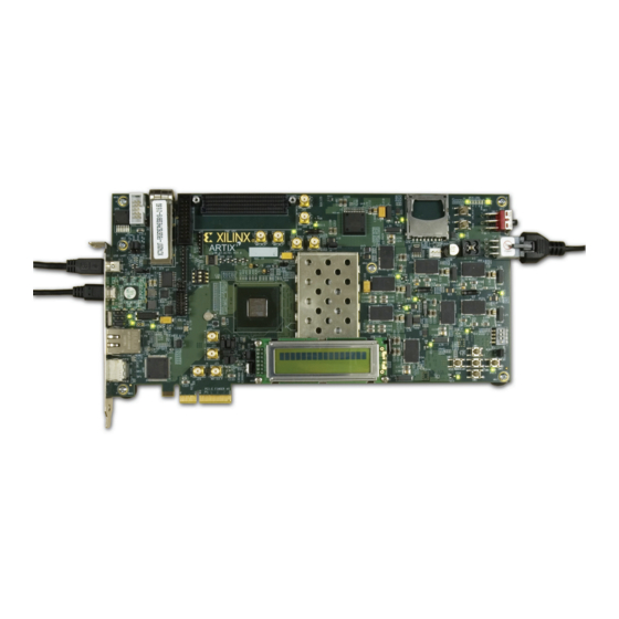
The built-in self-test (BIST), the AMS 101 evaluation card usage, and the Artix-7 FPGA Base Targeted Reference Design (TRD) are featured in this getting started guide. X-Ref Target - Figure 1 UG967_01_111412 Figure 1: AC701 Evaluation Kit AC701 Getting Started Guide www.xilinx.com Send Feedback UG967 (v4.0.1) March 05, 2014... -
Page 8: Basic Hardware Bring-Up With Built-In Self-Test
Table. Basic Hardware Bring-up with Built-In Self-Test Introduction The BIST reference design tests many of the features of the Artix-7 FPGA AC701 Evaluation Kit and can be programmed into the FPGA via the JTAG interface. www.xilinx.com AC701 Getting Started Guide Send Feedback UG967 (v4.0.1) March 05, 2014... - Page 9 Rotary switch (under LCD) Status LEDs and user LEDs CPU reset button Prog button Power slide switch 12V power connector User DIP switch Contrast wheel User push buttons USB-UART connector AC701 Getting Started Guide www.xilinx.com Send Feedback UG967 (v4.0.1) March 05, 2014...
- Page 10 (ON, OFF, ON = 101). X-Ref Target - Figure 3 ON Position = 1 M2 M1 M0 OFF Position = 0 UG967_03_102813 Figure 3: SW1 Switch Settings for JTAG Programming Mode www.xilinx.com AC701 Getting Started Guide Send Feedback UG967 (v4.0.1) March 05, 2014...
- Page 11 Set the USB-UART connection to a known PORT in the Device Manager: Right-click the Computer desktop icon and select Properties. b. Click Device Manager. Right-click the Cypress device in the list, and select Properties (see Figure AC701 Getting Started Guide www.xilinx.com Send Feedback UG967 (v4.0.1) March 05, 2014...
- Page 12 Download the AC701 BIST Design Files (RDF0220) from the AC701 Evaluation Kit Documentation webpage under the Example Designs section. Unzip the design files to the C:\ directory. Start the installed terminal program. www.xilinx.com AC701 Getting Started Guide Send Feedback UG967 (v4.0.1) March 05, 2014...
- Page 13 In Vivado Design Suite, open a Tcl shell and type: source C:/ac701_bist/ready_for_download/bist_download.tcl Select the desired tests to run and observe the test results (see Figure X-Ref Target - Figure 9 UG967_09_111412 Figure 9: BIST Main Menu AC701 Getting Started Guide www.xilinx.com Send Feedback UG967 (v4.0.1) March 05, 2014...
-
Page 14: Ams Bring-Up With The Ams101 Evaluation Card
ADC feature. The AC701 Evaluation Kit also includes voltage, current and power monitoring for nine of the analog power supplies on the board. For evaluation of Xilinx Analog Mixed Signal (AMS) capability, these items in the kit are needed: •... - Page 15 Click on Targeted Reference Designs. This will open a list of files and documents. d. Click on AMS Targeted Reference Design for Artix-7 FPGA AC701 Evaluation Kit (RDF0278) to download rdf0278-ams101-ac701-trd.zip. Unzip the files to a working directory on the host computer.
- Page 16 Open xadc_eval_design.bit from the AC701 board AMS design folder: xadc_eval_design_ac701_v1_0 > ready_to_test > xadc_eval_design.bit Open the AMS Evaluator tool. Running the setup program loads the AMS101 Evaluator GUI with the Xilinx logo on your desktop. Figure 11 shows the AMS101 Evaluator after opening. From here, click the Connect button.
- Page 17 In conjunction with the AMS Evaluator, the AC701 AMS reference design also measures the voltages, current and power for V , the 1.8V supply, the 3.3V supply, CCO_ADJ MGTAVCC and MGTAVTT. AC701 Getting Started Guide www.xilinx.com Send Feedback UG967 (v4.0.1) March 05, 2014...
- Page 18 AMS Bring-up with the AMS101 Evaluation Card X-Ref Target - Figure 13 UG967_13_112712 Figure 13: Voltage, Current and Power Monitoring on AC701 Board Supplies www.xilinx.com AC701 Getting Started Guide Send Feedback UG967 (v4.0.1) March 05, 2014...
-
Page 19: Advanced Bring-Up With Base Targeted Reference Design
125 MHz C2S1 Checker 128 bits at 125 MHz Generator Loopback Integrated Blocks Xilinx IP Third Party IP AXI ST (128 bits at 125 MHz) Control Path in FPGA On Board AXI MM (512 bits at 100 MHz) 50 MHz Domain... - Page 20 Built-in hardware to monitor power by reading the TI UCD90120A power controller chip included on the AC701 evaluation board • Built-in hardware to monitor die temperature by way of a Xilinx Analog-to-Digital Converter Test Setup Requirements The prerequisites for testing the design in hardware are •...
- Page 21 Table 4: AC701 Board Required Switch Settings Switch Function/Type Setting SW15 Board power slide-switch User GPIO DIP switch Positions 1, 2, and 3 set configuration mode 001 – Master SPI 101 – JTAG AC701 Getting Started Guide www.xilinx.com Send Feedback UG967 (v4.0.1) March 05, 2014...
- Page 22 Advanced Bring-up with Base Targeted Reference Design X-Ref Target - Figure 15 SW15 Pin 1 Pin 1 UG967_15_040513 Figure 15: AC701 Board Switch and Jumper Locations www.xilinx.com AC701 Getting Started Guide Send Feedback UG967 (v4.0.1) March 05, 2014...
- Page 23 PCIe connector. X-Ref Target - Figure 16 Figure 16: AC701 Board Installed in a PCIe x16 Connector AC701 Getting Started Guide www.xilinx.com Send Feedback UG967 (v4.0.1) March 05, 2014...
- Page 24 LED position 2: ON if the lane width is x4, else flashing • LED position 3: Heart beat LED, flashes if PCIe user clock is present • LED position 4: ON if the PCIe link is up www.xilinx.com AC701 Getting Started Guide Send Feedback UG967 (v4.0.1) March 05, 2014...
- Page 25 It might be necessary to adjust the PC BIOS boot order settings to ensure that the DVD-ROM drive is the first drive in the boot order. Refer to the PC user manual for the proper procedure to set the BIOS boot order. AC701 Getting Started Guide www.xilinx.com Send Feedback UG967 (v4.0.1) March 05, 2014...
- Page 26 The lspci command displays the PCI and PCI Express buses of the PC. On the bus corresponding to the PCIe connector holding the AC701 board, look for the message: Memory controller: Xilinx Corporation Device 7042 This message confirms that the design programmed into the AC701 board is detected by the BIOS and the Fedora 16 OS.
- Page 27 Advanced Bring-up with Base Targeted Reference Design Figure 20 shows an example of the output from the lspci command. The highlighted region shows that Xilinx device 7042 has been located by the BIOS on bus number 3 (03:00.0 = bus:dev.function). X-Ref Target - Figure 20...
- Page 28 Figure 22: Running the quickstart.sh Script The GUI showing driver installation options appears as shown in Figure Subsequent steps demonstrate the GUI operation by installing and removing drivers. Click Install. www.xilinx.com AC701 Getting Started Guide Send Feedback UG967 (v4.0.1) March 05, 2014...
- Page 29 Advanced Bring-up with Base Targeted Reference Design X-Ref Target - Figure 23 UG967_23_121812 Figure 23: Artix-7 FPGA Base TRD Driver Installation GUI AC701 Getting Started Guide www.xilinx.com Send Feedback UG967 (v4.0.1) March 05, 2014...
- Page 30 Upon successful installation of the drivers, the control and monitoring interface appears. GUI Control Function These parameters are controlled with the GUI: • Packet size for traffic generation. www.xilinx.com AC701 Getting Started Guide Send Feedback UG967 (v4.0.1) March 05, 2014...
- Page 31 The various GUI indicators and controls are detailed in Figure 25 Table X-Ref Target - Figure 25 UG967_25_111312 Figure 25: Control and Monitoring Interface AC701 Getting Started Guide www.xilinx.com Send Feedback UG967 (v4.0.1) March 05, 2014...
- Page 32 Power in Watt plotted for the VCCINT, GTVCC, VCCAUX, and Power statistics VCCBRAM rails Temperature Monitors the current die temperature Notes: 1. Items 2 through 5 are duplicated for each of the two datapaths. www.xilinx.com AC701 Getting Started Guide Send Feedback UG967 (v4.0.1) March 05, 2014...
- Page 33 Verify PCIe endpoint throughput. b. Verify the DMA Channel throughput for Datapath-0. Verify the DMA Channel throughput for Datapath-1. d. Verify that there are no buffer descriptor errors for error-free operation. AC701 Getting Started Guide www.xilinx.com Send Feedback UG967 (v4.0.1) March 05, 2014...
- Page 34 Design Suite must be installed before proceeding with custom modifications. The design tools do not need to be installed on the same host PC in which the AC701 evaluation board is installed. www.xilinx.com AC701 Getting Started Guide Send Feedback UG967 (v4.0.1) March 05, 2014...
-
Page 35: Appendix A: Additional Resources
AC701 Evaluation Kit Master Answer Record (AR 51900) Artix-7 FPGA Base Targeted Reference Design Master Answer Record (AR 53372) These Xilinx documents and sites provide supplemental material useful with this guide: AC701 Evaluation Board for the Artix-7 FPGA User Guide (UG952) -
Page 36: Additional References
Vivado Design Suite product page (Vivado ® Design Suite information and downloads ) Artix-7 FPGA Product Table (List of Artix®-7 FPGAs) Silicon Labs Si570, Si5324C, CP2103GM, VCP Drivers www.xilinx.com AC701 Getting Started Guide Send Feedback UG967 (v4.0.1) March 05, 2014... -
Page 37: Appendix B: Warranty
For any breach by Xilinx of this limited warranty, the exclusive remedy of Customer and the sole liability of Xilinx shall be, at the option of Xilinx, to replace or repair the affected products, or to refund to Customer the price of the affected products. The availability of replacement products is subject to product discontinuation policies at Xilinx. - Page 38 Appendix B: Warranty www.xilinx.com AC701 Getting Started Guide Send Feedback UG967 (v4.0.1) March 05, 2014...
Need help?
Do you have a question about the Artix-7 FPGA AC701 and is the answer not in the manual?
Questions and answers