
Subscribe to Our Youtube Channel
Related Manuals for Xilinx SP601


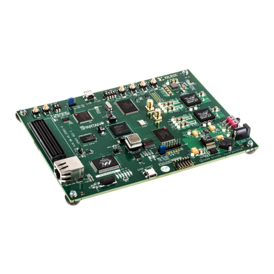
Summary of Contents for Xilinx SP601
- Page 1 SP601 Hardware User Guide [Guide Subtitle] [optional] UG518 (v1.1) August 19, 2009 [optional] UG518 (v1.1) August 19, 2009...
- Page 2 Xilinx. Xilinx expressly disclaims any liability arising out of your use of the Documentation. Xilinx reserves the right, at its sole discretion, to change the Documentation without notice at any time. Xilinx assumes no obligation to correct any errors contained in the Documentation, or to advise you of any corrections or updates.
-
Page 3: Revision History
Figure 1-32. • Updated Table 1-4, Table 1-17, and Table 1-20. • Added introductory paragraph to Appendix D, “SP601 Master UCF.” • Miscellaneous typographical edits and new user guide template. UG518 (v1.1) August 19, 2009 www.xilinx.com SP601 Hardware User Guide... - Page 4 SP601 Hardware User Guide www.xilinx.com UG518 (v1.1) August 19, 2009...
-
Page 5: Table Of Contents
Online Document ............8 Chapter 1: SP601 Evaluation Board Overview . - Page 6 Appendix A: References Appendix B: Default Jumper and Switch Settings Appendix C: VITA 57.1 FMC Connections Appendix D: SP601 Master UCF www.xilinx.com SP601 Hardware User Guide UG518 (v1.1) August 19, 2009...
-
Page 7: Preface: About This Guide
This manual contains the following chapters: • Chapter 1, “SP601 Evaluation Board,” provides an overview of the embedded development board and details the components and features of the SP601 board. • Appendix A, “References.” • Appendix B, “Default Jumper and Switch Settings.”... -
Page 8: Online Document
Blue text in the current document Refer to “Title Formats” in Chapter 1 for details. Go to http://www.xilinx.com Blue, underlined text Hyperlink to a website (URL) for the latest speed files. www.xilinx.com SP601 Hardware User Guide UG518 (v1.1) August 19, 2009... -
Page 9: Chapter 1: Sp601 Evaluation Board
The SP601 board enables hardware and software developers to create or evaluate designs targeting the Spartan®-6 XC6SLX16-2CSG324 FPGA. The SP601 provides board features for evaluating the Spartan-6 family that are common to most entry-level development environments. Some commonly used features include a DDR2 memory controller, a parallel linear flash, a tri-mode Ethernet PHY, general- purpose I/O (GPIO), and a UART. -
Page 10: Features
Chapter 1: SP601 Evaluation Board Features The SP601 board provides the following features: • 1. Spartan-6 XC6SLX16-2CSG324 FPGA • 2. 128 MB DDR2 Component Memory • 3. SPI x4 Flash • 4. Linear Flash BPI • 5. 10/100/1000 Tri-Speed Ethernet PHY •... -
Page 11: Block Diagram
External Config UG518_01_070809 Figure 1-1: SP601 Features and Banking Related Xilinx Documents Prior to using the SP601 Evaluation Board, users should be familiar with Xilinx resources. See the following locations for additional documentation on Xilinx tools and solutions: • ISE: www.xilinx.com/ise... -
Page 12: Detailed Description
Chapter 1: SP601 Evaluation Board Detailed Description Figure 1-2 shows a board photo with numbered features corresponding to Table 1-1 the section headings in this document. X-Ref Target - Figure 1-2 14 14 13 13 15 15 16 16 11 11... -
Page 13: Spartan-6 Xc6Slx16-2Csg324 Fpga
Cypress USB to JTAG download cable 14, 15 logic Onboard Power Power Management 11,12,13 1. Spartan-6 XC6SLX16-2CSG324 FPGA A Xilinx Spartan-6 XC6SLX16-2CSG324 FPGA is installed on the Embedded Development Board. Configuration The SP601 supports configuration in the following modes: • Master SPI x4 •... -
Page 14: Mb Ddr2 Component Memory
2. 128 MB DDR2 Component Memory There are 128 MB of DDR2 memory available on the SP601 board. A 1-Gb Elpida EDE1116ACBG (84-ball) DDR2 memory component is accessible through Bank 3 of the LX16 device. The Spartan-6 FPGA hard memory controller is used for data transfer across the DDR2 memory interface's 16-bit data path using SSTL18 signaling. - Page 15 DDR2_A5 DDR2_A6 DDR2_A7 DDR2_A8 DDR2_A9 DDR2_A10 DDR2_A11 DDR2_A12 DDR2_DQ0 DDR2_DQ1 DDR2_DQ2 DDR2_DQ3 DDR2_DQ4 DDR2_DQ5 DDR2_DQ6 DDR2_DQ7 DDR2_DQ8 DDR2_DQ9 DDR2_DQ10 DQ10 DDR2_DQ11 DQ11 DDR2_DQ12 DQ12 DDR2_DQ13 DQ13 DDR2_DQ14 DQ14 DDR2_DQ15 DQ15 SP601 Hardware User Guide www.xilinx.com UG518 (v1.1) August 19, 2009...
- Page 16 Chapter 1: SP601 Evaluation Board Table 1-5: DDR2 Component Memory Connections (Cont’d) Memory U2 FPGA U1 Schematic Netname Pin Number Name DDR2_BA0 DDR2_BA1 DDR2_BA2 DDR2_WE_B DDR2_RAS_B DDR2_CAS_B DDR2_ODT DDR2_CLK_P DDR2_CLK_N DDR2_CKE DDR2_LDQS_P LDQS DDR2_LDQS_N LDQS DDR2_UDQS_P UDQS DDR2_UDQS_N UDQS DDR2_LDM...
- Page 17 Figure 1-5: UCF Location Constraints for DDR2 SDRAM Control Pins References See the Elpida DDR2 specifications for more information at http://www.elpida.com/en/products/details/EDE1116ACBG.html. Also, see the Spartan-6 FPGA embedded hard memory controller block user guide at http://www.xilinx.com/support/documentation/user_guides/ug388.pdf. SP601 Hardware User Guide www.xilinx.com UG518 (v1.1) August 19, 2009...
-
Page 18: Spi X4 Flash
Chapter 1: SP601 Evaluation Board 3. SPI x4 Flash The Xilinx Spartan-6 FPGA hosts a SPI interface which is visible to the Xilinx iMPACT configuration tool. The SPI memory device operates at 3.0V; the Spartan-6 FPGA I/Os are 3.3V tolerant and provide electrically compatible logic levels to directly access the SPI flash through a 2.5V bank. - Page 19 SPI MEM U17 SPI HDR J12 FPGA U1 Schematic Netname Pin # Pin Name Pin # Pin Name FPGA_PROG_B FPGA_D2_MISO3 IO3_HOLD_B FPGA_D1_MISO2_R IO2_WP_B SPI_CS_B FPGA_MOSI_CSI_B_MISO0 FPGA_D0_DIN_MISO_MISO1 IO1_DOUT FPGA_CCLK VCC3V3 J15.2 SPIX4_CS_B CS_B SP601 Hardware User Guide www.xilinx.com UG518 (v1.1) August 19, 2009...
-
Page 20: Linear Flash Bpi
Chapter 1: SP601 Evaluation Board Figure 1-8 provides the UCF constraints for the SPI serial flash PROM. X-Ref Target - Figure 1-8 NET "FPGA_D2_MISO3" LOC = "V14"; NET "SPI_CS_B" LOC = "V3"; NET "FPGA_D0_DIN_MISO_MISO1" LOC = "R13"; NET "FPGA_D1_MISO2" LOC = "T14";... - Page 21 FLASH_A7 FLASH_A8 FLASH_A9 FLASH_A10 FLASH_A11 FLASH_A12 FLASH_A13 FLASH_A14 FLASH_A15 FLASH_A16 FLASH_A17 FLASH_A18 FLASH_A19 FLASH_A20 FLASH_A21 FLASH_A22 FLASH_A23 FLASH_A24 FPGA_D0_DIN_MISO_MISO1 FPGA_D1_MISO2 FPGA_D2_MISO3 FLASH_D3 FLASH_D4 FLASH_D5 FLASH_D6 FLASH_D7 FLASH_WE_B WE_B FLASH_OE_B OE_B SP601 Hardware User Guide www.xilinx.com UG518 (v1.1) August 19, 2009...
- Page 22 Figure 1-10: UCF Location Constraints for BPI Flash Connections References See the Numonyx Flash Memory specifications for more information at http://www.numonyx.com/Documents/Datasheets/308551_J3D_Discrete_DS.pdf. In addition, see the Xilinx Spartan-6 Configuration User Guide for more information at http://www.xilinx.com/support/documentation/user_guides/ug380.pdf. www.xilinx.com SP601 Hardware User Guide...
-
Page 23: 100/1000 Tri-Speed Ethernet Phy
Detailed Description 5. 10/100/1000 Tri-Speed Ethernet PHY The SP601 uses the onboard Marvell Alaska PHY device (88E1111) for Ethernet communications at 10, 100, or 1000 Mb/s. The board supports a GMII/MII interface from the FPGA to the PHY. The PHY connection to a user-provided Ethernet cable is through a Halo HFJ11-1G01E RJ-45 connector with built-in magnetics. - Page 24 Chapter 1: SP601 Evaluation Board Table 1-9: PHY Connections (Cont’d) FPGA U1 Schematic Netname U3 M88E111 PHY_RXD7 PHY_TXC_GTXCLK PHY_TXCLK PHY_TXER PHY_TXCTL_TXEN PHY_TXD0 PHY_TXD1 PHY_TXD2 PHY_TXD3 PHY_TXD4 PHY_TXD5 PHY_TXD6 PHY_TXD7 X-Ref Target - Figure 1-11 NET "PHY_COL" LOC = "L14"; NET "PHY_CRS"...
-
Page 25: Usb-To-Uart Bridge
The SP601 contains a Silicon Labs CP2103GM USB-to-UART bridge device (U4) which allows connection to a host computer with a USB cable. The USB cable is supplied in this evaluation kit (Type A end to host computer, Type Mini-B end to SP601 connector J9). Table 1-10 details the SP601 J9 pinout. -
Page 26: Iic Bus
UG518_13_070809 Figure 1-13: IIC Bus Topology The IIC Bus on the SP601 provides access to a 2-pin header, the onboard 8-Kb EEPROM, and the VITA 57.1 FMC interface. The user must ensure there are no IIC address conflicts with the onboard EEPROM address when attaching additional IIC devices via FMC or the IIC 2-pin header. -
Page 27: 8-Kb Nv Memory
8. Clock Generation There are three clock sources available on the SP601 . Oscillator (Differential) The SP601 has one 2.5V LVDS differential 200 MHz oscillator (U5) soldered onto the board and wired to an FPGA global clock input. • Crystal oscillator: Epson EG2121CA •... -
Page 28: Oscillator Socket (Single-Ended, 2.5V Or 3.3V)
Oscillator Socket (Single-Ended, 2.5V or 3.3V) One populated single-ended clock socket (X2) is provided for user applications. The option of 3.3V or 2.5V power may be selected via a 0 ohm resistor selection. The SP601 board is shipped with a 27MHz 2.5V oscillator installed. - Page 29 LA14_N LA15_N LA17_P_CC LA20_P LA17_N_CC LA19_P LA20_N LA18_P_CC LA19_N LA23_P LA18_N_CC LA22_P LA23_N LA21_P LA22_N LA21_N LA26_P LA27_P LA25_P LA26_N LA27_N LA24_P LA25_N LA24_N LA29_P LA28_P LA29_N LA28_N 3P3VAUX LA31_P SP601 Hardware User Guide www.xilinx.com UG518 (v1.1) August 19, 2009...
- Page 30 Chapter 1: SP601 Evaluation Board Table 1-13: LPC Pinout (Cont’d) LA30_P LA31_N TRST_L LA30_N 12P0V LA33_P 3P3V LA32_P LA33_N 12P0V LA32_N 3P3V VADJ 3P3V VADJ 3P3V www.xilinx.com SP601 Hardware User Guide UG518 (v1.1) August 19, 2009...
- Page 31 NET "FMC_LA33_N" LOC = "N9"; NET "FMC_LA33_P" LOC = "M10"; NET "FMC_PRSNT_M2C_L" LOC = "U13"; NET "FMC_PWR_GOOD_FLASH_RST_B" LOC = "B3"; Figure 1-18: UCF Location Constraints for VITA 57.1 FMC-LPC Connections SP601 Hardware User Guide www.xilinx.com UG518 (v1.1) August 19, 2009...
-
Page 32: Status Leds
Chapter 1: SP601 Evaluation Board 10. Status LEDs Table 1-14 defines the status LEDs. Table 1-14: Status LEDs Reference Signal Name Color Label Description Designator Indicates power available for FMC_PWR_GOOD_ VITA 57.1 FMC expansion Green FLASH_RST_B GOOD connector. PHY_LED_LINK10 Green... -
Page 33: Fpga Awake Led And Suspend Jumper
NET "FPGA_AWAKE" LOC = "P15"; NET "FPGA_SUSPEND" LOC = "R16"; Figure 1-20: UCF Location Constraints for FPGA Awake/Suspend Mode Jumper See the Spartan-6 FPGA Configuration Guide for more information at http://www.xilinx.com/support/documentation/user_guides/ug380.pdf. SP601 Hardware User Guide www.xilinx.com UG518 (v1.1) August 19, 2009... -
Page 34: Fpga Init And Done Leds
The typical Xilinx FPGA power up and configuration status LEDs are present on the SP601. The INIT LED DS10 comes on after the FPGA powers up and completes its internal power-on process. The DONE LED DS9 comes on after the FPGA programming bitstream has been downloaded and the FPGA successfully configured. -
Page 35: User I/O
Detailed Description 13. User I/O The SP601 provides the following user and general purpose I/O capabilities: • User LEDs • User DIP switch • Pushbutton switches • CPU Reset pushbutton switch • GPIO male pin header Note: Figure 1-27 All GPIO location constraints are collected in one partial UCF in... - Page 36 Label FPGA Pin Designator DS13 GPIO_LED_2 Green DS14 GPIO_LED_3 Green User DIP switch The SP601 includes an active high four pole DIP switch, as described in Figure 1-24 Table 1-18. X-Ref Target - Figure 1-24 VCC2V5 GPIO_SWITCH_0 GPIO_SWITCH_1 GPIO_SWITCH_2 GPIO_SWITCH_3 SDMX-4-X 4.7K...
- Page 37 Detailed Description User Pushbutton Switches The SP601 provides five active high pushbutton switches: SW6, SW4, SW5, SW7 and SW9. The five pushbuttons all have the same topology as the sample shown in Figure 1-25. Four pushbuttons are assigned as GPIO, and the fifth is assigned as a CPU_RESET.
- Page 38 Chapter 1: SP601 Evaluation Board GPIO Male Pin Header The SP601 provides a 2X6 GPIO male pin header supporting 3.3V power, GND and eight I/Os. Figure 1-26 Table 1-20 describe the J13 GPIO Male Pin Header. X-Ref Target - Figure 1-26...
- Page 39 NET "GPIO_HDR4" LOC = "F15"; NET "GPIO_HDR5" LOC = "B4"; NET "GPIO_HDR6" LOC = "F13"; NET "GPIO_HDR7" LOC = "P12"; Figure 1-27: UCF Location Constraints for User and General-Purpose I/O SP601 Hardware User Guide www.xilinx.com UG518 (v1.1) August 19, 2009...
-
Page 40: Fpga_Prog_B Pushbutton Switch
AC Adapter and 5V Input Power Jack/Switch The SP601 is powered from a 5V source that is connected through a 2.1mm x 5.5mm type plug (center positive). SP601 power can be turned on or off through a board mounted slide switch. - Page 41 Power Management The SP601 uses power solutions from LTC. An estimate of the current draw on the various power supply rails is shown in Table 1-22. X-Ref Target - Figure 1-30 Monolithic Regulator Jack 0.9V@3A max Dual Switcher LTM4616 3. 3V@8A max 2.
-
Page 42: Configuration Options
JTAG Configuration JTAG configuration is provided through onboard USB-to-JTAG configuration logic where a computer host accesses the SP601 JTAG chain through a Type-A (computer host side) to Type-Mini-B (SP601 side) USB cable. The JTAG chain of the board is illustrated in Figure 1-31. - Page 43 FPGA's SPI or BPI interface. Through the connection made by the temporary design in the FPGA, iMPACT can indirectly program the SPI flash or BPI flash from the JTAG USB J10 connector. SP601 Hardware User Guide www.xilinx.com UG518 (v1.1) August 19, 2009...
- Page 44 Chapter 1: SP601 Evaluation Board www.xilinx.com SP601 Hardware User Guide UG518 (v1.1) August 19, 2009...
- Page 45 This section provides references to documentation supporting Spartan-6 FPGAs, tools, and IP. For additional information, see www.xilinx.com/support/documentation/index.htm. Documents supporting the SP601 Evaluation Board: UG138, LogiCORE™ IP Tri-Mode Ethernet MAC v4.2 User Guide UG380, Spartan-6 FPGA Configuration User Guide UG381, Spartan-6 FPGA SelectIO Resources User Guide UG388, Spartan-6 FPGA Memory Controller User Guide DS614, Clock Generator (v3.01a) Data Sheet...
- Page 46 Appendix A: References www.xilinx.com SP601 Hardware User Guide UG518 (v1.1) August 19, 2009...
- Page 47 Appendix B Default Jumper and Switch Settings Table B-1 shows the default jumper and switch settings for the SP601. Table B-1: Default Jumper and Switch Settings REFDES Type/Function Default SLIDE, POWER ON-OFF DIP, 2-POLE, MODE ON (1) OFF (0) DIP, 4-POLE, GPIO...
- Page 48 Appendix B: Default Jumper and Switch Settings www.xilinx.com SP601 Hardware User Guide UG518 (v1.1) August 19, 2009...
- Page 49 FMC_LA09_P FMC_LA18_CC_P FMC_LA09_N FMC_LA18_CC_N FMC_LA13_P FMC_LA27_P FMC_LA13_N FMC_LA27_N FMC_LA17_CC_P IIC_SCL_MAIN FMC_LA17_CC_N IIC_SDA_MAIN FMC_LA23_P FMC_LA23_N FMC_LA26_P FMC_LA26_N FMC_CLK1_M2C_P FMC_PRSNT_M2C_L FMC_CLK1_M2C_N FMC_CLK0_M2C_P FMC_LA00_CC_P FMC_CLK0_M2C_N FMC_LA00_CC_N FMC_LA02_P FMC_LA03_P FMC_LA02_N FMC_LA03_N FMC_LA04_P FMC_LA08_P FMC_LA04_N SP601 Hardware User Guide www.xilinx.com UG518 (v1.1) August 19, 2009...
- Page 50 FMC_LA11_P FMC_LA16_P FMC_LA11_N FMC_LA16_N FMC_LA15_P FMC_LA20_P FMC_LA15_N FMC_LA20_N FMC_LA19_P FMC_LA22_P FMC_LA19_N FMC_LA22_N FMC_LA21_P FMC_LA25_P FMC_LA21_N FMC_LA25_N FMC_LA24_P FMC_LA29_P FMC_LA24_N FMC_LA29_N FMC_LA28_P FMC_LA31_P FMC_LA28_N FMC_LA31_N FMC_LA30_P FMC_LA33_P FMC_LA30_N FMC_LA33_N FMC_LA32_P FMC_LA32_N www.xilinx.com SP601 Hardware User Guide UG518 (v1.1) August 19, 2009...
- Page 51 Appendix D SP601 Master UCF The UCF template is provided for designs that target the SP601. Net names provided in the constraints below correlate with net names on the SP601 rev. C schematic. On identifying the appropriate pins, the net names below should be replaced with net names in the user RTL.
- Page 52 Appendix D: SP601 Master UCF NET "DDR2_LDQS_P" LOC = "L4"; NET "DDR2_ODT" LOC = "K6"; NET "DDR2_RAS_B" LOC = "L5"; NET "DDR2_UDM" LOC = "K4"; NET "DDR2_UDQS_N" LOC = "P1"; NET "DDR2_UDQS_P" LOC = "P2"; NET "DDR2_WE_B" LOC = "E3";...
- Page 53 NET "FMC_PRSNT_M2C_L" LOC = "U13"; NET "FMC_PWR_GOOD_FLASH_RST_B" LOC = "B3"; NET "FPGA_AWAKE" LOC = "P15"; NET "FPGA_CCLK" LOC = "R15"; NET "FPGA_CMP_CLK" LOC = "U16"; NET "FPGA_CMP_CS_B" LOC = "P13"; SP601 Hardware User Guide www.xilinx.com UG518 (v1.1) August 19, 2009...
- Page 54 Appendix D: SP601 Master UCF NET "FPGA_CMP_MOSI" LOC = "V16"; NET "FPGA_D0_DIN_MISO_MISO1" LOC = "R13"; NET "FPGA_D1_MISO2" LOC = "T14"; NET "FPGA_D2_MISO3" LOC = "V14"; NET "FPGA_DONE" LOC = "V17"; NET "FPGA_HSWAPEN" LOC = "D4"; NET "FPGA_INIT_B" LOC = "U3";...
- Page 55 NET "SYSCLK_P" LOC = "K15"; NET "USB_1_CTS" LOC = "U10"; NET "USB_1_RTS" LOC = "T5"; NET "USB_1_RX" LOC = "L12"; NET "USB_1_TX" LOC = "K14"; NET "USER_CLOCK" LOC = "V10"; SP601 Hardware User Guide www.xilinx.com UG518 (v1.1) August 19, 2009...
Need help?
Do you have a question about the SP601 and is the answer not in the manual?
Questions and answers