Table of Contents

Related Manuals for ADLINK Technology cPCI-6810


Summary of Contents for ADLINK Technology cPCI-6810
- Page 1 Series 6U CompactPCI Dual/Single Pentium TM III SBC and Rear I/O Transition Modules User’s Manual 2.01 Manual Rev. Revision Date: December 21, 2006 50-15016-201 Part No: Advance Technologies; Automate the World.
- Page 2 Copyright 2005 ADLINK TECHNOLOGY INC. All Rights Reserved. The information in this document is subject to change without prior notice in order to improve reliability, design, and function and does not represent a commitment on the part of the manufacturer.
- Page 3 Getting Service from ADLINK Customer Satisfaction is top priority for ADLINK Technology Inc. Please contact us should you require any service or assistance. ADLINK TECHNOLOGY INC. Web Site: http://www.adlinktech.com Sales & Service: Service@adlinktech.com TEL: +886-2-82265877 FAX: +886-2-82265717 Address: 9F, No. 166, Jian Yi Road, Chungho City,...
-
Page 5: Table Of Contents
Universal Serial Bus (USB) ........... 13 Serial I/O ............... 13 Keyboard/Mouse Controller .......... 13 Specifications..............14 Specifications of cPCI-6820 front board ....... 14 Specifications of cPCI-R6820 RTM ......17 Common Spec. for cPCI-6810/6820 and RTM ..... 18 Model Variations ..............22 Table of Contents... - Page 6 / 6810 Board Outline and Illustration....26 cPCI-6820 Top and Front View ........26 cPCI-6820 Model comparison table ......27 cPCI-6810 Top and Front View ........28 cPCI-6810 Model comparison table ......29 cPCI-R6820 Board Outline and Illustration ......30 cPCI-R6820 Top and Front View ........
- Page 7 4 Device Driver Installation ..........57 VGA Drivers Installation............. 58 Driver Installation on Windows NT ........ 58 Driver Installation on Red Hat Linux 7.3 ....... 59 LAN Drivers Installation ............. 60 Software and Drivers Support ........60 Driver Installation on Windows 2000/XP ....... 60 5 Appendix ................
-
Page 8: List Of Tables
Table 1-2: PMC Options ............11 Table 1-3: Power Requirement (Typical) ......... 19 Table 1-4: I/O Connectivity ............21 Table 1-5: CPCI-6810/6820 Model Variations Table ....22 Table 1-6: Recommended PMC Modules ........ 23 Table 1-7: Recommended Chassis .......... 23 Table 2-1: Comparison of cPCI-6820A and cPCI-6820B .. - Page 9 List of Figures Figure 1-1: cPCI-6810/6820 Block Diagram ........ 5 Figure 2-1: Top and Front View of cPCI-6820 ......26 Figure 2-2: Top and Front View of cPCI-6810 ......28 Figure 2-3: Top and front View of cPCI-R6820......30 List of Figures...
-
Page 11: Introduction
The cPCI-6820 board features dual Intel® Pentium® III Processor - Low Power (933 MHz) with 512KB L2 cache, while the cPCI-6810 is based on the same architecture as the cPCI-6820 but features only a single Intel® Pentium® III Processor - Low Power (933 MHz). -
Page 12: Checklist
The CPU configurations can be single or dual CPU. cPCI-6810 or cPCI-6820 Front Board The cPCI-6810/6820 CPU module may be equipped with different capacities of RAM, HDD, and PCM depending on requirements. Please check the configurations with your dealer and check that the package is complete and contain the items below. -
Page 13: Cpci-R6820 Rtm
RTM The cPCI-R6820 is designed to provide additional I/O functionality through rear I/O connectivity for the cPCI-6820 or cPCI-6810. The cPCI-R6810 can be shipped with or without a storage device (IDE HDD or CF card) depending on the options ordered. Please check possible configurations with your dealer. -
Page 14: Cpci-R6820 Features
PICMG 2.0 CompactPCI Specification R3.0 Compliant 6U form factor, 1-slot (4TE/HP) in width, 80mm in board depth Designed for cPCI-6810 and 6820 series front board Supports dual RJ-45 GbE connectors, onboard dual EIDE interfaces with CF socket and housing for onboard 2.5” ATA... -
Page 15: Functional Block
1.3 Functional Block Figure 1-1: cPCI-6810/6820 Block Diagram Introduction... -
Page 16: Compactpci Bus Interface
System Slot supporting a host, or as a Non-Transparent bridge in a Peripheral Slot as an intelligent subsystem. These options allow the cPCI-6810/6820 board to be inserted into both the Peripheral Slot and the System Slot. In addition to the 66MHz/64bit capability, the host bus and subsystem bus can operate at different speeds. -
Page 17: Bios
HB6 bridge. BIOS The cPCI-6810/6820 adopts the Award BIOS with a 4Mb flash ROM implemented to load the BIOS. A boot block device is used to allow recovery of the BIOS in the event of a catastrophic failure (power failure during BIOS update). -
Page 18: Processor
Processor The cPCI-6810/6820 motherboard is based on the RCC/ ServerWorks Champion LE chipset and supports a single or dual Intel Mobile Pentium III processor – M. The supported CPU package is a micro-FCBGA. The Intel® Pentium® III processor - Low Power is a 0.18-micron product, which is a highly integrated assembly with all its immediate system-level support. -
Page 19: Interrupts
Max. Memory 1.5GB 1.5GB Table 1-1: cPCI-6810/6820 Memory Configurations Interrupts Two enhanced interrupt controllers provide the cPCI-6810/6820 with a total of 15 interrupt inputs. Interrupt controller features include support for: Level-triggered and edge-triggered inputs Individual input masking Fixed and rotating priorities... -
Page 20: Dma
Two enhanced DMA controllers are provided on the cPCI-6810/ 6810 for use by onboard peripherals. The cPCI-6810/6820's DMA controllers reside in the CNB30LE device. Real-Time Clock The super I/O PC87417 provides DS1287 compatible Real-Time Clock. It provides a Y2K compliant century calendar as well as a time of day function. -
Page 21: Power Ramp Circuitry
Power Ramp Circuitry The cPCI-6810/6820 features a power controller with power ramp circuitry to allow the board's voltages to be ramped in a controlled fashion. The power ramp circuitry eliminates any large voltage or current spikes caused by hot-swap boards. This controlled ramping is a requirement of the CompactPCI hot-swap specification, PICMG 2.1, Version 1.0. -
Page 22: Ethernet Interfaces
The CRT interconnections are available on both the front panel of cPCI-6820 and rear I/O board. IDE Interface The fast IDE interface on cPCI-6810/6820 supports up to four IDE devices including hard disk drives and CD ROMS. Each IDE device can have independent timing. The IDE interface supports PIO IDE transfers of up to 14MB/sec. -
Page 23: Universal Serial Bus (Usb)
Transfer speeds of up to 24Mb/s are supported. The cPCI-6810/6820 provides the standard 0.5A at 5V to the peripherals. The power to each port is protected by a single polyswitch (this current rating allows for inrush currents). -
Page 24: Specifications
1.4 Specifications Specifications of cPCI-6820 front board CompactPCI Compliancy PICMG 2.0 CompactPCI core specification R3.0 PICMG 2.1 CompactPCI hot-swap R1.0 PICMG 2.16 CompactPCI packet switching backplane (cPSB) R1.0 PICMG 2.9 System Management Bus R1.0 PCI Rev 2.1 compliant Form Factor Standard 6U CompactPCI (board size: 233.35 x160mm2) Single-slot (4 TE/HP, 20.32mm) width, incl. - Page 25 BIOS: ADLINK Enhanced Award / Phoenix BIOS Support Intel® Pre-boot Execution Environment (PXE) version 2.x, WFM 2.0. Include BIOS setup options and boot from LAN Support DMI / SMBIOS 2.3 CPU, memory operating frequency auto-detection Bootable from USB storage devices including USB-Floppy, USB-ZIP USB-CD-ROM and USB-HDD.
- Page 26 PS2 keyboard and mouse connector: cPCI-6820: With 6-pin circular DIN connectors on both the front board and RTM. cPCI-6810: Connectors on RTM only. Built-in W82782D monitoring CPU temperatures, FAN speed, system temperature, V core, and DC voltages. Watchdog timer: Programmable I/O port 10h-12h of bank 3 to configure watchdog timer, programmable 8-bit timer 1 - 255 minutes.
-
Page 27: Specifications Of Cpci-R6820 Rtm
backup by a separate 3V coin cell battery (PANSONIC CR2032 or compatible). IPMI Interface Supports PICMG 2.9 secondary system managing bus. Implements IPMI functions as defined in the IPMI specification v1.0. Qlogic Zircon CP Baseboard Management Controller (BMC) with 14KB internal SRAM, 1MB external flash ROM. Front Panel LED Indicators and Reset Four LEDs on the front panel including storage access LED (RED), Power LED (GREEN), hot-swap status (Blue), and... -
Page 28: Common Spec. For Cpci-6810/6820 And Rtm
44-pin connector for 2.5” HDD. Secondary IDE supported on one 40-pin IDE connector and one CompactFlash type-II socket. Common Spec. for cPCI-6810/6820 and RTM Flash Storage Support Options DiskOnModule via the 40-pin IDE on RTM, 16 - 256MB. CompactFlash card via the CF socket on RTM, 8 - 12MB. -
Page 29: Table 1-3: Power Requirement (Typical)
Note: Certified with ADLINK thermal design. The thermal performance is dependent on the cooling design. Temperature limit of optional mass storage devices may have an impact on the thermal specification of the board. Operational vibration is limited by the 2.5 inch HDD. - Page 30 Typical Current and +3.3V +12V -12V Maximum Current (+/-5%) (+/-5%) (+/-5%) (+/-5%) cPCI-6810A/1G 1.44A 3.64A (Without PMC, VGA 3.73A 14.636A cards & RTM) cPCI-6810/1G 3.16A 4.76A with HDD 3.88A+HDD 14.636A 2.66A 4.36A cPCI-6820A/P9 3.73A 16.526A cPCI-6820A/P9 3.56A 5.36A with HDD 3.73A+HDD 16.526A...
-
Page 31: Table 1-4: I/O Connectivity
I/O Connectivity cPCI-6820 cPCI-6810 RTM (cPCI-R6820) Faceplate Board Faceplate Board J3/J5 Faceplate Board Serial Port RJ-45 RJ-45 (COM1) Serial Port 10-pin (COM2) Header PS2 Keyboard PS2 Mouse DB-15 DB-15 USB (port 0, USB x 2 USB x 2 port 1) -
Page 32: Model Variations
1.5 Model Variations The cPCI-6810/6820 series products include the following four base configurations. All models have the CPU pre-mounted. The number of SO-DIMM sockets and PMC slots are varied depending on the model. If a HDD is installed onboard, it may occupy and sacrifice one PMC socket space. -
Page 33: Table 1-6: Recommended Pmc Modules
Single Port 32-bit/33MHz Fast Ethernet PMC card PMC-8670 Port80 Display PMC card Table 1-6: Recommended PMC Modules The following table lists the recommended chassis available from ADLINK, which are compatible with the cPCI-6810/6820 series SBC. Chassis Description / Configuration cPCIS-6130R 19”... -
Page 35: Jumpers And Connectors
Jumpers and Connectors This chapter will familiarize the user with the cPCI-6810/6820 before getting started; information on the board layout, connector definitions, and jumper setup is provided. It also includes the following information: cPCI-6810/6820 board outline and illustration cPCI-R6820 board outline and illustration... -
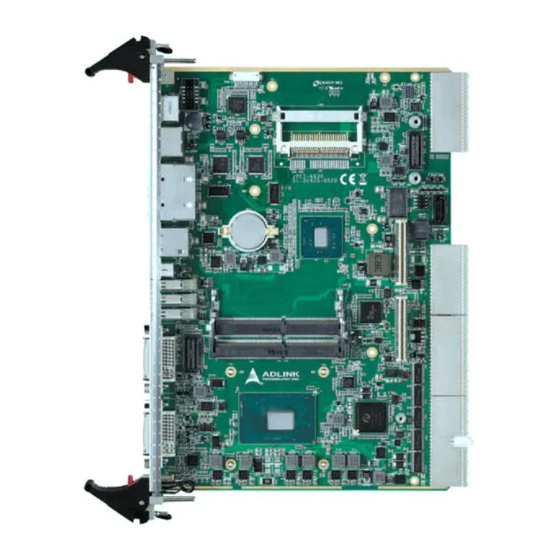
Page 36: Cpci-6820 / 6810 Board Outline And Illustration
2.1 cPCI-6820 / 6810 Board Outline and Illustration cPCI-6820 Top and Front View Figure 2-1: Top and Front View of cPCI-6820 Jumpers and Connectors... -
Page 37: Cpci-6820 Model Comparison Table
cPCI-6820 Model comparison table cPCI-6820A/P9 cPCI-6820B/P9 No. of Memory sockets SO-DIMM 1,2 Dual SODIMM Dual SODIMM SO-DIMM 3,4 Single SODIMM Dual SODIMM (1) Max. Memory 1.5GB 2.0GB HDD Installation Possible Not Feasible (1) PMC slot# (without HDD) PMC slot# (with HDD) 0 (2) Table 2-1: Comparison of cPCI-6820A and cPCI-6820B Note:... -
Page 38: Cpci-6810 Top And Front View
Top and Front View Figure 2-2: Top and Front View of cPCI-6810 Jumpers and Connectors... -
Page 39: Cpci-6810 Model Comparison Table
Model comparison table cPCI-6810A/P9 cPCI-6810B/P9 No. of Memory sockets SO-DIMM 1, 2 Single SODIMM Dual SODIMM (1) SO-DIMM 3, 4 Single SODIMM Single SODIMM Max. Memory 1.0GB 1.5GB HDD Installation Possible Possible PMC slot# (without HDD) 1 (1) PMC slot# (with HDD) -
Page 40: Cpci-R6820 Board Outline And Illustration
2.2 cPCI-R6820 Board Outline and Illustration cPCI-R6820 Top and Front View Figure 2-3: Top and front View of cPCI-R6820 Jumpers and Connectors... -
Page 41: Connectors Pin Assignment
Ground Power KBCLK Keyboard Clock No connect Table 2-3: Keyboard Connector Note: Circular DIN keyboard connector is available on the cPCI-6820 only. The cPCI-6810 does not support a keyboard connector. Mouse Connector Signal Function MSDATA Mouse Data No Connect Ground... -
Page 42: Keyboard And Mouse Combo Connector
Keyboard and Mouse Combo Connector Signal Function KBDATA Keyboard Data MSDATA Mouse Data Ground Power KBCLK Keyboard Clock MSCLK Mouse Clock Table 2-5: Keyboard and Mouse Combo Connector Note: Keyboard and Mouse Combo Connector is available on the cPCI-R6820 RTM only. A Y-cable is shipped with the RTM and can be used to connect a PS/2 keyboard mouse... -
Page 43: Table 2-7: Com1 On Rtm
Serial Port on 10-pin Header Connector Signal Name DCD: Data Carrier Detect RXD: Receive Data TXD: Transmit Data DTR: Data Terminal Ready Ground DSR: Data Set Ready RTS: Request to Send CTS: Clear to Send RI: Ring Indicate No Connect Table 2-7: COM1 on RTM Jumpers and Connectors... -
Page 44: Vga Connector
VGA Connector Signal Name Signal Name Green Blue N.C. +5V. N.C. N.C. HSYNC VSYNC Table 2-8: TVGA Connector on cPCI-6820 and RTM USB Connector Signal Name USB- USB+ Ground Table 2-9: USB Connector LED for Gigabit Ethernet Ports Color Status Description 10 or 100 Mbps Link Speed LED... -
Page 45: General Purpose Led Definitions
General Purpose LED definitions Color Status Description IDE idle IDE Media Access IDE access System is not power- on or power failed Power OK Green Power ON Board inserted and power on Hot swap- Blue pable status Board inserted but not power on yet Table 2-11: General Purpose LED definitions Speaker connector on RTM... -
Page 46: 44-Pin Ide Port
44-pin IDE Port Signal Signal RESET- Ground DD10 DD11 DD12 DD13 DD14 DD15 Ground N.C (key pin) DMARQ Ground DIOW- Ground DIOR- Ground IORDY CSEL DMACK- Ground INTRQ reserved PDIAG- CS0- CS1- DASP- Ground Ground TYPE- Table 2-13: 44-pin IDE connector Note: Primary IDE is on the front board (CN8) on the RTM. -
Page 47: 40-Pin Ide Port
40-pin IDE Port Signal Signal RESET- Ground DD10 DD11 DD12 DD13 DD14 DD15 Ground +5V (for DOM) DMARQ Ground DIOW- Ground DIOR- Ground IORDY CSEL DMACK- Ground INTRQ reserved PDIAG- CS0- CS1- DASP- Ground Table 2-14: 40-pin Primary and Secondary IDE channels on the RTM Jumpers and Connectors... -
Page 48: Ipmb Interface On Rtm
IPMB Interface on RTM Signal Name IPMB_CLK IPMB_DATA IPMB_PWR Table 2-15: IPMI Interface on RTM The IPMB interface is connected to the rJ5 of the RTM. The IPMB_PWR is connected to pin-C1 of the rJ5. Jumpers and Connectors... -
Page 49: Compactpci J1 Pin Assignments
CompactPCI J1 Pin Assignments REQ64# +3.3V ENUM# AD [1] V (I/O) AD [0] ACK64# +3.3V AD [4] AD [3] AD [2] AD [7] +3.3V AD [6] AD [5] +3.3V AD [9] AD [8] M66EN C/BE [0]# AD [12] V (I/O) AD [11] AD [10] +3.3V... - Page 50 Note: (1) These signals are not connected. (2) These signals are pulled high on the board. (3) These signals are pulled low on the board. (4) As a peripheral CPU, ENUM# is automatically driven during insertion or extraction to support PICMG 2.1 hot-swap.
-
Page 51: Compactpci J2 Pin Assignments
CompactPCI J2 Pin Assignments CLK6 BRSV BRSV BRSV CLK5 BRSV BRSV IPMBSDA IPMBSCL IPMBALR BRSV BRSV BRSV BRSV PRST# REQ6# GNT6# BRSV DEG# BRSV BRSV BRSV FAL# REQ5# GNT5# BRSV AD [35] AD [34] AD [33] AD [32] AD [38] V (I/O) AD [37] AD [36]... -
Page 52: Compactpci J3 And Rj3 Pin Assignments
CompactPCI J3 and rJ3 Pin Assignments +12V -12V GND LPa_DA0+ LPa_DA0- LPa_DC0+ LPa_DC0- GND GND LPa_DB0+ LPa_DB0- LPa_DD0+ LPa_DD0- GND GND LPb_DA1+ LPb_DA1- LPb_DC1+ LPb_DC1- GND GND LPb_DB1+ LPb_DB1- LPb_DD1+ LPb_DD1- GND +3.3V +3.3V +3.3V PMCIO5 PMCIO4 PMCIO3 PMCIO2 PMCIO1 PMCIO10 PMCIO9 PMCIO8... -
Page 53: Compactpci J5 And Rj5 Pin Assignments
CompactPCI J5 and rJ5 Pin Assignments CS3- DASP- DIOW- DMACK- DIOR- PDIAG- DD15 INTRQ DMARQ IORDY DD12 DD13 DD14 DD10 DD11 DRESET- USB-0+ USB-0- USB-1+ USB-1- SMUX SMUX SMUX SMUX SMUX SMUX SMUX SMUX +3.3V +3.3V DDCCLK DDCDAT VSYNC HSYNC BLUE GREEN USB-2+... - Page 54 Note: (1) The pins are reserved with no connection. (2) The 3.3V and 5V power lines are supplied from the main board to the RTM. (3) USB_OC is the USB over-current feedback from the RTM to main board. (4) The SMUX signals are used for serial COM port extension.
-
Page 55: Pmc Connector Pin Assignments
PMC Connector Pin Assignments PMC J11/J21 and J12/J22 Connector Pin Assignments Signal J11/J21 J11/J21 Signal Signal J12/J22 J12/J22 Signal Name Name Name Name -12V +12V TRST# INTA# INTB# INTC# INTD# +3.3V +3.3V CLKP1 RST# GNT0# +3.3V REQ0# PME# AD31 AD30 AD29 AD28 AD27... -
Page 56: Table 2-21: Pmc J13/J23 And J24 Connector Pin Assignments
PMC J13/J23 and J24 Connector Pin Assignments J13/ J13/ Signal Signal Signal Signal Name Name Name Name PMCIO1 PMCIO2 CBE [7] PMCIO3 PMCIO4 CBE [6] CBE [6] PMCIO5 PMCIO6 CBE [5] PMCIO7 PMCIO8 PAR64 PMCIO9 PMCIO10 AD63 AD62 PMCIO11 PMCIO12 AD61 PMCIO13 PMCIO14... -
Page 57: Ide Setting Jumper On The Rtm
Note: (1) These signals are not connected on the board. (2) These signals are pulled high on the board. (3) These signals are pulled low on the board. (4) By default, the VIO signals are set to +5V via zero ohm resistors. Therefore, DO NOT apply any “3.3V only”... -
Page 58: Gbe Connection Selection
GbE Connection Selection The cPCI-6820 supports dual Ethernet connection for PICMG2.16 compliant backplanes and the RTM. While using the PICMG 2.16 compliant backplane, it is recommended that none of the GbE ports on the rear panel be used. There are four mini switches that control the GbE routing located on the bottom side (solder side) of the RTM. -
Page 59: Setting Jumper On Cpci-6810/6820
A 3-pin jumper (JP1) is used to set the SBC as either “in normal operation” or “forcing the SBC to SYSTEM mode”. Note: When cPCI-6810/6820 in the Packet Switching Backplane has no PCI bus, set JP1 as “1-2”. Normal operation (Default setting) -
Page 60: Table 2-24: Setting Jumper On Cpci-6810/6820
Signal Name SYSEN# Table 2-24: Setting Jumper on cPCI-6810/6820 Jumpers and Connectors... -
Page 61: Getting Started
It will cause board defects and void all warranty for the board. 3.2 Memory Module Installation The cPCI-6810/6820 SBC supports up to four sockets of 144-pin PC-133 registered ECC SO-DIMMs. The maximum memory capacity is therefore 2GB. If memory modules are pre-installed when the package is received, this section can be skipped. -
Page 62: Table 3-1: Supported Sdram Chip
The chipset supports 64Mb, 128Mb, 256Mb, and 512Mb memory technologies. The supported DRAM types are listed in the following table. DRAM Depth DRAM Type (Row/Column) 11/9 16M 2-bank SDRAM 11/10 64M 2-bank SDRAM 13/10 12/8 12/9 64M 4-bank SDRAM 12/10 13/10 12/9 12/10... -
Page 63: Hdd Installation On Main Board
3.3 HDD Installation on Main Board A slim-type 2.5-inch HDD can be mounted to the cPCI-6810/6820 main board. If a HDD comes pre-installed in the cPCI-R6820 product package, this section may be skipped. 1. Remove the PMC Key-bolt of the PMC slot #1. -
Page 64: Pci Mezzanine Card (Pmc) Installation
With the cPCI-6810/6820, the CF card is very easy to use; the CF card socket is available on the cPCI-R6820, which is a rear transition module. 3.6 PCI Mezzanine Card (PMC) Installation The PMC slots are designed as 5V and / or as a universal PCI interface. -
Page 65: Main Board Installation
DO NOT access these ports on both front and rear simultaneously. 3.8 Main Board Installation Follow the instructions below to install the cPCI-6810/6820 main board to its CompactPCI chassis. 1. Refer to the relevant chassis user manual for pre-... -
Page 67: Device Driver Installation
Device Driver Installation To install the drivers for the cPCI-8610/8620, refer to the installation information in this chapter. Basic information is presented in this section, however, for more detailed installation information for non-Windows Operating Systems, refer to the extensive explanation inside the ADLINK CD. The drivers are located in the following directories of the CD-ROM: VGA/AGP driver \CHIPDRV\VGA\69000... -
Page 68: Vga Drivers Installation
4.1 VGA Drivers Installation This section describes the VGA driver installation for the onboard VGA controller M69000. The relative drivers are located in X:\CHIPDRV\VGA\69000 directory of the ADLINK CD: where X: is the location of the CD-ROM drive. The VGA drivers for Windows 98/95, Windows NT, and Windows 2000 are included. -
Page 69: Driver Installation On Red Hat Linux 7.3
Driver Installation on Red Hat Linux 7.3 The standard Linux installation procedure will install the graphic driver for the VGA chip. However, under Red Hat Linux 7.3 or higher, the standard VGA driver is not fully compatible with the C&T69000 VGA chip. The installation of Red Hat Linux 7.3 may hang after entering X-Windows. -
Page 70: Lan Drivers Installation
4.2 LAN Drivers Installation This chapter describes the LAN driver installation for the onboard Ethernet controller Intel 82546EB. All associated drivers are located under following ADLINK directory: X:\CHIPDRV\LAN\82546EB, where X: is the location of the CD- ROM drive. Software and Drivers Support The 82546EB drivers support the following OS or platforms: Windows 2000, Windows XP All of the above drivers are included on the ADLINK CD. -
Page 71: Appendix
Appendix Appendix A - IPMI Functions List The following table lists the IPMI V1.0 functions that are supported by the cPCI-6810 and cPCI-6820. CPCI-6820 IPMI V1.0 Function List CPCI-6810 IPM Device “Global” Commands √ Get Device ID √ Cold Reset √... - Page 72 CPCI-6820 IPMI V1.0 Function List CPCI-6810 √ Get BT Interface Capabilities √ Get System GUID Chassis Device Commands √ Get Chassis Status √ Chassis Control √ Get POH Counter Event Commands √ Set Event Receiver √ Get Event Receiver Platform Event (a.k.a. “Event Message”)
- Page 73 CPCI-6820 IPMI V1.0 Function List CPCI-6810 √ Read FRU Data √ Write FRU Data SDR Device Commands √ Get SDR Repository Info √ Get SDR Repository Allocation Info √ Reserve SDR Repository √ Get SDR √ Add SDR √ Partial Add SDR √...
-
Page 74: Ipmi Address Map
Note: (1) Supported on PCB rev.A3 or higher. (2) The SDR information are read-only. (3) The SEL storage is not supported random access. Not available means that an additional onboard EEPROM is required to store information. This requires a modification of the A3 version board - the A2 version board does not have the EEPROM. -
Page 75: Appendix B - Watchdog Timer Programming Guide
Appendix B - WatchDog Timer Programming Guide The Watchdog Timer (WDT) can monitor the system’s status. Once a value is given to the WDT, the timer will begin to count down. If the system becomes idle or hangs, the system will reboot itself when the timer times out. -
Page 76: Wdt Setup Instructions
WDT Setup Instructions 1. Set pin 55 of PC87417 as Watch Dog Timer output pin Set Bit 7 of SIOCF2 Register (Index: 22H) to 1, for example: o 2E 22 o 2F 80 2. Set Logic Device to System Wake-Up Control (SWC) Set Logic Device Number Register (Index: 07H) to 04H, for example: o 2E 07... - Page 77 6. Select Bank 3 for Watch Dog Timer from SWC base address. Set Bit 1-0 of BANKSEL Register (I/O Base: 840H, Offset: 0FH) to 11, for example: o 84F 03 7. Set the count down value for Watch Dog timer. ->...
-
Page 78: Appendix C - Power Consumption
Appendix C - Power Consumption Hardware Environment: Single or Dual LV P-III 933M or 1GHz Memory: 1GB (512MB x 2) or 1.5GB (512MBx3) HDD: FUJITSU MHR2040AT 40GB installed on RTM (Max. current requirement is 0.55A @ +5V CompactFlash: PQI 64MB Flash Card PMC card: ADLINK PMC-8615 Gigabit Ethernet Card PMC VGA card: ADLINK PMC-8217V (only available with CRUX-SP) - Page 79 3.73A+HDD 14.636A 2.50A 4.10A cPCI-6810A/1G 3.88A 14.636A cPCI-6810A/1G (Without 1.44A 3.64A PMC, VGA cards, and RTM) 3.73A 14.636A 3.16A 4.76A cPCI-6810/1G with HDD 3.88A+HDD 14.636A 2.66A 4.36A cPCI-6820A/P9 3.73A 16.526A 3.56A 5.36A cPCI-6820A/P9 with HDD 3.73A+HDD 16.526A 3.38A 4.98A cPCI-6820B/1G 3.88A...
-
Page 80: Appendix D - Smbus Address Map
Appendix D - SMBus Address Map The SMBus address Map on the cPCI-6820 products are as follows: Address Function Device (Hex) 0x A0 SO-DIMM ID(1) SO-DIMM 0x 5C Hardware Monitor ADM1026 0x AC SEL data storage (IPMI) 24C64 0x AE FRU data storage (IPMI) 24C64 0x AA... -
Page 81: Warranty Policy
Warranty Policy Thank you for choosing ADLINK. To understand your rights and enjoy all the after-sales services we offer, please read the follow- ing carefully. 1. Before using ADLINK’s products please read the user man- ual and follow the instructions exactly. When sending in damaged products for repair, please attach an RMA appli- cation form which can be downloaded from: http:// rma.adlinktech.com/policy/. - Page 82 3. Our repair service is not covered by ADLINK's guarantee in the following situations: Damage caused by not following instructions in the User's Manual. Damage caused by carelessness on the user's part dur- ing product transportation. Damage caused by fire, earthquakes, floods, lightening, pollution, other acts of God, and/or incorrect usage of voltage transformers.
Need help?
Do you have a question about the cPCI-6810 and is the answer not in the manual?
Questions and answers