Table of Contents

Related Manuals for ADLINK Technology cPCI-3915B


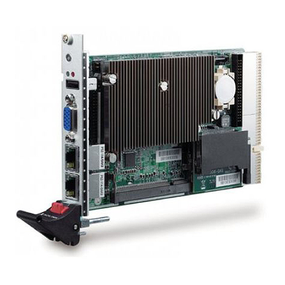
Summary of Contents for ADLINK Technology cPCI-3915B
- Page 1 cPCI-3915 Series 3U CompactPCI Single Board Computers with Intel® Pentium® M/Intel® Celeron® M Processors User’s Manual Manual Rev. 2.00 Revision Date: June 30, 2006 Part No: 50-15055-1000 Advance Technologies; Automate the World.
- Page 2 Copyright 2006 ADLINK TECHNOLOGY INC. All Rights Reserved. The information in this document is subject to change without prior notice in order to improve reliability, design, and function and does not represent a commitment on the part of the manufacturer.
- Page 3 Getting Service from ADLINK Customer Satisfaction is top priority for ADLINK Technology Inc. Please contact us should you require any service or assistance. ADLINK TECHNOLOGY INC. Web Site: http://www.adlinktech.com Sales & Service: Service@adlinktech.com TEL: +886-2-82265877 FAX: +886-2-82265717 Address: 9F, No. 166, Jian Yi Road, Chungho City,...
- Page 5 Table of Contents Table of Contents..............i List of Tables................iv List of Figures ................. v 1 Overview ................1 Introduction ................1 Features................1 Board Diagram..............2 Product List................3 SBC ................3 Transition module ............3 Package contents ..............3 CPU module ..............
- Page 6 Hardware Monitor .............. 16 PCI Resource Allocation ............ 16 4 Jumpers and Connectors..........17 cPCI-3915 Series Board Outline........18 cPCI-3915A ..............18 cPCI-3915B ..............18 cPCI-R3915 ..............19 cPCI-3915 PCB Layout ..........20 DB-3915CF PCB Layout ..........21 DB-3915L2 PCB Layout ..........22 cPCI-R3915 PCB Layout ..........
- Page 7 Installing the Hard Disk Drive ..........44 CF Card Installation ............46 Installing the cPCI-3915 to the Chassis......47 RTM (cPCI-R3915) Installation.......... 48 6 Windows® Driver Installation ......... 49 7 Utilities ................51 Watch Dog Timer............... 51 Using the Watchdog in an Application ....... 52 Intel®...
- Page 8 List of Tables Table 2-1: Power consumption of Intel® Pentium® M ....9 Table 2-2: Power consumption of Intel® Celeron® M ....9 Table 3-1: PCI Resource Allocation ......... 16 List of Tables...
- Page 9 List of Figures Figure 1-1: cPCI-3915 Block Diagram ......... 2 Figure 5-1: CPU Installation............40 Figure 5-2: Heat Sink Installation..........42 Figure 5-3: Memory Installation ..........43 Figure 5-4: 2.5” Hard Disk Installation ........46 Figure 5-5: Compact Flash Card Installation ......47 Figure 7-1: cPCI-3915 Watch Dog Timer Architecture ....
- Page 10 List of Figures...
-
Page 11: Overview
The cPCI-3915 is a 3U CompactPCI single board computer that comes in two compact PCI form factors: single-slot cPCI-3915A and dual-slot cPCI-3915B. Featuring support for single Intel® Cel- eron® M processor with 1 MB L2 cache or Intel® Pentium® M pro- cessor with 2 MB L2 cache in µFC-PGA package, the cPCI-3915... -
Page 12: Board Diagram
1.3 Board Diagram Figure 1-1: cPCI-3915 Block Diagram Overview... -
Page 13: Product List
M/Celeron® M processor with dual GbE, single USB, and CRT output (assembled with DB-3915CF daughter board) cPCI-3915B: Dual-slot 3U SBC featuring Intel® Pentium® M/Celeron® M processor with dual GbE, dual USB, dual COM, and CRT output (assembled with DB-3915L2 and... - Page 14 *CPU, memory, and HDD specifications may vary depending on the selected configuration Note: The contents of non-standard cPCI-3915 configurations may vary depending on the customer’s requirements. CAUTION: This product must be protected from static discharge and physical shock. Never remove any of the components except at a static-free workstation.
-
Page 15: Specifications
Specifications 2.1 CPU, memory, and chipset Intel® Pentium® M 1.5 GHz to 2.0 GHz processor in µFC- PGA package, 90 nm process with 2 MB L2 cache Processor Intel® Celeron® M 1.3 GHz to 1.5 GHz processor in µFC- PGA package, 90nm process with 1 MB L2 cache Front side bus 400/533 MHz Up to 1 GB system memory using single non-ECC DDR2... -
Page 16: Software
cPCI-3915 module Single-channel SATA port DB-3915CF daughter board Single channel, ATA100/66/33 IDE connector (44-pin) Board I/O interfaces Hot-swappable CompactFlash slot cPCI-R3915 rear transition module DVI transmitter Single-channel SATA port Single-channel LVDS connector 1 x USB 2.0 port 1 x DVI port Rear panel I/O 1 x RS-232 port (supports RS-232, RS-422, RS-485, or RS-485+ via jumper setting) - Page 17 Shock 15G peak-to-peak, 11ms duration, non-operation Vibration Non-operating: 1.88G rms, 5 to 500 Hz, each axis Operating: 0.5G rms. 5 to 500 Hz, each axis, with 2.5” HDD and CompactFlash card Compliance CE, FCC Class A Specifications...
-
Page 18: I/O Connectivity Table
2.5 I/O Connectivity Table cPCI-3915A cPCI-3915B cPCI-R3915 Faceplate Board Faceplate Board Faceplate Board Y (DB-15) Y (DB-15) Y (DVI-I) LVDS Y(RJ-45) x 2 Y(RJ-45) x 2 Y x 1 Y x 2 Y x 1 Y (Combo) COM1 Y (DB-9) -
Page 19: Table 2-1: Power Consumption Of Intel® Pentium® M
Power Voltage +3.3V +12V -12V Total Light-loading 13.93W 12.65W 0.17W 0.36W 27.11W Full-loading 15.15W 29.15W 0.11W 0.6W 45.01W Table 2-1: Power consumption of Intel® Pentium® M Power Voltage +3.3V +12V -12V Total Light-loading 13.93W 8.6W 0.17W 0.36W 23.06W Full-loading 15.15W 19.1W 0.11W 0.6W 34.96W Table 2-2: Power consumption of Intel®... - Page 20 Specifications...
-
Page 21: Functional Description
Functional Description The following sections describe the cPCI-3915 main functions. 3.1 Processor The cPCI-3915 supports a single Intel® Pentium® M/Intel® Cele- ron® M processor with 2 MB/1 MB L2 cache in µFC-PGA pack- age. The Intel® Pentium® M/Intel® Celeron® M processor is a high-performance, low-power mobile processor with several enhancements over previous mobile processors. -
Page 22: Memory
3.3 Memory The cPCI-3915 supports a single-channel, unbuffered, non-ECC DDR2 SDRAM operating at 533/400 MHz. The GMCH supports a 128 MB, 256 MB, 512 MB, or 1 GB memory module in SODIMM package. The memory interface supports the following: 256 MB, 512 MB,and 1 GB technology supported using x8 or x16 devices High-density memory package for DDR2 type devices 128 MB minimum memory, 1 GB maximum memory... -
Page 23: I/O Controller Hub (Ich6-M)
3.6 I/O Controller Hub (ICH6-M) The ICH6-M provides extensive I/O support, including: PCI Express® base specification Revision 1.0a-compliant. PCI local bus specification, Revision 2.3 with support for 33 MHz PCI operations ACPI Power Management Logic Support Enhanced DMA controller, interrupt controller, and timer functions Integrated Serial ATA host controller with independent DMA operation on two ports and AHCI support... -
Page 24: Lpc/ Firmware Hub
naling. The cPCI-3915 comes with three USB 2.0 ports: one each on the cPCI-3915 board, DB-3915L2 daughter board on the cPCI- R3915 board. All USB ports implement over-current detection and support USB floppy boot. USB legacy devices, such as keyboard, mouse, and floppy drive are supported and can be enabled or dis- abled in the BIOS. -
Page 25: Pci Express® Interface
using I/O space and AHCI mode using memory space. The Intel® ICH6-M supports the Serial ATA Specification Revision 1.0a on two SATA ports. The SATA ports are located on the cPCI-3915 board and cPCI-R3915 board. 3.7 PCI Express® Interface The Intel® ICH6-M supports four PCI Express® root ports compli- ant with the PCI Express Base Specification Revision 1.0a. -
Page 26: Hardware Monitor
3.8 Hardware Monitor The IT8712F chip monitors several critical hardware parameters, including system and CPU voltages and temperatures. All hard- ware status information can be viewed and configured through the BIOS menu, and run-time utilities. Once the preset thresholds of hardware conditions reach critical limits, the IT8712F alerts or resets the system. -
Page 27: Jumpers And Connectors
Jumpers and Connectors This chapter illustrates the board layout, connector pin assign- ments, and jumper settings to familiarize the users on the cPCI- 3915. Jumpers and Connectors... -
Page 28: Cpci-3915 Series Board Outline
4.1 cPCI-3915 Series Board Outline cPCI-3915A cPCI-3915B Jumpers and Connectors... -
Page 29: Cpci-R3915
cPCI-R3915 Jumpers and Connectors... -
Page 30: Cpci-3915 Pcb Layout
cPCI-3915 PCB Layout LAN (88E8052) B North Bridge (915GM) K DDR2 DIMM SOCKET C South Bridge (ICH6-M) L SATA CONNECTOR SIO (IT8712F) USB Connector N To DB-3915L2 Connector VGA Connector O To DB-3915CF Connector LAN Connector cPCI J1 LAN Connector cPCI J2 LAN (88E8052) Jumpers and Connectors... -
Page 31: Db-3915Cf Pcb Layout
DB-3915CF PCB Layout BATTERY HOLDER BUZZER CF SOCKET D 44 PINS IDE CONNECTOR TO MB CONNECTOR Select CF Master/Slave Jumpers and Connectors... -
Page 32: Db-3915L2 Pcb Layout
DB-3915L2 PCB Layout USB CONNECTOR B KB/MS COMBO CONNECTOR RS232 CONNECTOR RS232 CONNECTOR TO M/B CONNECTOR Jumpers and Connectors... -
Page 33: Cpci-R3915 Pcb Layout
cPCI-R3915 PCB Layout cPCI J2 RS232 CONNECTOR B SATA CONNECTOR G Header for Select COM PORT type C LVDS CONNECTOR H Header for Select COM PORT type DVI CONNECTOR I Header for Select COM PORT type E USB CONNECTOR J Header for Select COM PORT type Jumpers and Connectors... -
Page 34: Connector Pin Assignments
4.2 Connector Pin Assignments USB Connectors Pin # Signal Name USB- USB+ Ethernet (RJ-45) Connector Pin # Signal Name Function GBE0_MDI0+ Media Dependent Interface 0+ GBE0_MDI0- Media Dependent Interface 0- GBE0_MDI1+ Media Dependent Interface 1+ GBE0_MDI1- Media Dependent Interface 1- GBE0_MDI2+ Media Dependent Interface 2+ GBE0_MDI2- Media Dependent Interface 2- GBE0_MDI3+ Media Dependent Interface 3+... - Page 35 Left LED Right LED Status (Green) (Amber or Green) Network link is not established 10 Mbps Link Green (10 BaseT) Active Blink Green 100 Mbps Link Green Green (100BaseTX) Active Blink Green Green 1000 Mbps Link Green Amber (1000 BaseT) Active Blink Green Amber...
-
Page 36: Vga Connector
VGA Connector Signal Name Pin # Pin # Signal Name Green Blue N.C. +5V. N.C. CRTDATA HSYNC VSYNC CRTCLK RS-232 DB-9 Serial Port Connector (COM1, COM2) Pin # RS-232 DCD, Data carrier detect RXD, Receive data TXD, Transmit data DTR, Data terminal ready IsoGND, Isolated ground DSR, Data set ready Jumpers and Connectors... - Page 37 RTS, Request to send CTS, Clear to send RI, Ring indicator Jumpers and Connectors...
-
Page 38: Sata Connector
SATA Connector Pin # Signal Pin # Signal IDE Connector Signal Name Pin # Pin # Signal Name BRSTDRVJ DDP7 DDP8 DDP6 DDP9 DDP5 DDP10 DDP4 DDP11 DDP3 DDP12 DDP2 DDP13 DDP1 DDP14 DDP0 DDP15 Jumpers and Connectors... - Page 39 PDDREQ PDIOWJ PDIORJ PIORDY PCSEL PDDACKJ IRQ14 DAP1 DIAG DAP0 DAP2 CS1P CS3PJ IDEACTPJ Jumpers and Connectors...
-
Page 40: Dvi Connector
DVI Connector Pin # Signal Pin # Signal TX2- HTPLG TX2+ TX0- TX0+ DDCCLK DDCDATA VSYNC TXC+ TX1- TXC- TX1+ GREEN BLUE HSYNC Jumpers and Connectors... -
Page 41: Ps2 Connector
PS2 Connector Pin # Signal Function KBDATA Keyboard Data MSDATA Mouse Data Ground Power KBCLK Keyboard Clock MSCLK Mouse Clock Jumpers and Connectors... -
Page 42: Compactflash Connector
CompactFlash Connector Signal Name Pin # Pin # Signal Name DD11 DD12 DD13 DD14 DD15 CS1J CS3J SDIORJ SDIOWJ IRQ15 PCSEL Jumpers and Connectors... - Page 43 BRSTDRVJ SDIORDY SDACKJ IDEACTJ DIAG IOIS16J DD10 Jumpers and Connectors...
-
Page 44: General Purpose Led Definitions
General Purpose LED definitions Color Status Description IDE or SATA HDD Idle IDE or SATA HDD Access System power off or power failure PW/ WD GREEN System Power on BLINK Watch Dog Timer enabled To DB-3915L2 Connector Pin # Pin Name Pin # Pin Name USB1_OC-L... -
Page 45: To Db-3915Cf Connector
To DB-3915CF Connector Pin# Pin Name Pin# Pin Name BRSTDRV0J CONN_IDE_D8 CONN_IDE_D7 CONN_IDE_D9 CONN_IDE_D6 CONN_IDE_D10 CONN_IDE_D5 CONN_IDE_D11 CONN_IDE_D4 CONN_IDE_D12 CONN_IDE_D3 CONN_IDE_D13 CONN_IDE_D2 CONN_IDE_D14 CONN_IDE_D1 CONN_IDE_D15 CONN_IDE_D0 VBAT_DAUG PDDRQ PCSEL RPDIOWJ SPKR RPDIQRJ CPIORDY PDDAKJ PDA2 CIRQ14 RCS3PJ PDA1 PDA0 RCS1PJ SIO_SPKR IDEACTPJ Jumpers and Connectors... -
Page 46: Compactpci J1 Pin Assignment
CompactPCI J1 Pin Assignment REQ64# ENUM# +3.3V AD[1] AD[0] ACK64# GND +3.3V AD[4] AD[3] AD[2] AD[7] +3.3V AD[6] AD[5] +3.3V AD[9] AD[8] C/ BE[0]# GND AD[12] AD[11] AD[10] +3.3V AD[15] AD[14] AD[13] SERR# +3.3V C/ BE[1]# GND +3.3V PERR# DEVSEL# STOP# LOCK# +3.3V... -
Page 47: Compactpci J2 Pin Assignment
CompactPCI J2 Pin Assignment 22 GND 21 GND USB2_N USB2_P 20 GND USB2_OC-L 19 GND SATA_RXN2 SATA_RXP2 18 GND SATA_TXN2 SATA_TXP2 17 GND N12V 16 GND LA_DATAN2 LA_DATAP2 P12V 15 GND 14 GND LA_DATAN1 LA_DATAP1 13 GND P3V3 LA_DATAN0 LA_DATAP0 12 GND CRT_DDC_DATA LA_CLKN... -
Page 48: Rs-232, Rs-422, Rs-485, Rs-485+ Select Jumper
JP1 Select 1-2 CF Slave 2-3 CF Master RS-232, RS-422, RS-485, RS-485+ Select Jumper Refer to the jumper settings below before installing RS-232, RS- 422, RS-485, or RS-485+ devices. RS-232 1-2, 4-5 1-2, 4-5 1-2 RS-422 2-3, 5-6 2-3, 5-6 3-4 1-2, 4-5 RS-485 2-3, 5-6 5-6 1-2, 4-5 RS-485+ 2-3, 5-6... -
Page 49: Installing The Cpu And Heatsink
Getting Started This chapter explains installation of the following components to the cPCI-3915: CPU and heat sink Memory module 2.5” hard disk drive CF card CPU module 5.1 Installing the CPU and Heatsink The cPCI-3915 supports single Intel® Pentium® M/ Intel® Cele- ron®... -
Page 50: Figure 5-1: Cpu Installation
Figure 5-1: CPU Installation Getting Started... -
Page 51: Heat Sink Installation
Heat Sink Installation To install the heat sink: 1. Remove the film on top of the thermal pads. Refer to Fig- ure 5-2: Heat Sink Installation. 2. Place the heat sink on top of the CPU and Northbridge, making sure that the thermal pads has proper contact with the components. -
Page 52: Installing A Memory Module
Figure 5-2: Heat Sink Installation 5.2 Installing a Memory Module The cPCI-3915 supports one unbuffered, non-ECC DDR2 SDRAM in 200-pin SODIMM package. If the cPCI-3915 comes with a pre- installed memory module, proceed to the next section. Note: When installing a memory module, make sure that the mod- ule is firmly seated on the slot and does not interfere with any component. -
Page 53: Figure 5-3: Memory Installation
Figure 5-3: Memory Installation Getting Started... -
Page 54: Installing The Hard Disk Drive
5.3 Installing the Hard Disk Drive The cPCI-3195 supports a slim-type 2.5” HDD. If the cPCI-3195 comes with a pre-installed HDD, proceed to the next section. To install the hard disk drive: 1. Install the provided HDD bracket to the board. 2. - Page 55 Getting Started...
-
Page 56: Cf Card Installation
Figure 5-4: 2.5” Hard Disk Installation 5.4 CF Card Installation The CompactFlash card has been widely accepted in mission crit- ical embedded applications for its anti-shock/-vibration properties, better environmental tolerance, low power consumption, small form factor, and reliability. To install the CF card, insert it to the CF card slot located under the HDD. -
Page 57: Installing The Cpci-3915 To The Chassis
Figure 5-5: Compact Flash Card Installation 5.5 Installing the cPCI-3915 to the Chassis To install the cPCI-3915 module to a CompactPCI chassis: 1. Refer to the chassis documentation before installing the cPCI-3915. 2. Turn off the power in both chassis front and rear. 3. -
Page 58: Rtm (Cpci-R3915) Installation
6. Move the locking handle inward until it is fully-latched. A slight resistance may be felt when inserting the board. If the resistance is too strong, check if there are bent pins on the backplane or if the board’s connector pins are properly aligned with the connectors on the backplane. -
Page 59: Windows® Driver Installation
Windows® Driver Installation The cPCI-3915 drivers are available from the ADLINK All-In-One CD or from the ADLINK website (http://www.adlinktech.com). The following describes the driver installation procedures for Win- dows® 2000, Windows® XP or Windows® Server 2003: 1. Install the Windows operating system before installing any driver. - Page 60 Windows® Driver Installation...
-
Page 61: Utilities
Utilities 7.1 Watch Dog Timer This section explains the operation of the cPCI-3915’s watch dog timer (WDT). The primary function of the WDT is to monitor the cPCI-3915 operation and to reset the system if a software applica- tion fails to function as programmed. The following WDT functions may be controlled using a software application: enabled and disabled reloading timeout value... -
Page 62: Using The Watchdog In An Application
When the watch dog timed out, it will send a RESET signal to the system. 7.2 Using the Watchdog in an Application The following section describes the WDT functions in an applica- tion. The WDT reset function is explained in the previous section. This can be controlled through the registers in the cPCI Super I/O chip. -
Page 63: Bios Setup Introduction
BIOS 8.1 BIOS Setup Introduction The Phoenix-AwardBIOS provides a setup utility program for specifying the system configurations and settings. The BIOS ROM of the system stores the setup utility. When you turn on the com- puter, the BIOS is immediately activated. Pressing the <Del> or <Tab>... -
Page 64: Standard Cmos Features
The BIOS also supports to store the CMOS settings into non-vola- tile ROM by using F6/F7 key. Note: 1. After making and saving system changes with setup, you find that your computer cannot boot, the BIOS supports an override to the CMOS settings that resets your system to its default. - Page 65 battery fails, or the configuration stored in the CMOS memory was lost or damaged. At the bottom of the menu are the control keys for use on this menu. If you need any help in each item field, you can press the <F1>...
- Page 66 To set the date, highlight the “Date” field and use the <PgUp>/ <PgDn> or +/- keys to set the current time. Time The time format is: Hour 00 to 23 Minute 00 to 59 Second 00 to 59 To set the time, highlight the "Time" field and use the <PgUp>/ <PgDn>...
- Page 67 The following describes each item of this menu. IDE HDD Auto-Detection This item is used to detect the type of hard drive. It will assign the cylinder, head, precomp, landing zone, and sector to the hard drive.
- Page 68 Onboard PATA Master/Onboard PATA Slave/Onboard SATA-0/ Onboard SATA-1 Auto BIOS will auto detect the hard disk type. Manual User can assigns the type of hard disk when the access mode is normal. None Selects this selection when there is no hard disk in the system. Access Mode Auto Auto-detect the HDD mode...
- Page 69 Halt On This field determines whether the system will halt if an error is detected during power up. No Errors The system boot will not be halted for any error that may be detected. Whenever the BIOS detects a non-fatal error, the system will stop and All Errors you will be prompted.
-
Page 70: Advanced Bios Features
8.3 Advanced BIOS Features This section allows you to configure and improve your system and allows you to set up some system features according to your pref- erence. Hard Disk Boot Priority These items have a sub-menu when user press enter key. This item can lists all Hard Disk Device. - Page 71 CPU L1 & L2/L3 Cache Cache memory is additional memory that is much faster than conventional DRAM (system memory). CPUs with 486 proces- sors and upwards contain internal cache memory, and most, but not all, modern PCs have additional (external) cache mem- ory.
- Page 72 The A20 signal controlled by keyboard controller or Normal chipset hardware Typematic Rate Setting Enabled Enable typematic rate and typematic delay programming Disable typematic rate and typematic delay program- Disabled ming. The system BIOS will use default value of these 2 items and the default controlled by keyboard Typematic Rate (Chars/Sec) When the typematic rate is enabled, the system registers...
- Page 73 MPS version 1.4 added extended configuration tables to improve support for multiple PCI bus configurations and improve future expandability. Most newer versions of server operating system support MPS 1.4 and, as such, you should change the BIOS setup from the default of 1.1 to 1.4 if your operating system supports the 1.4 version.
-
Page 74: Advanced Chipset Features
Agent Wait Time(min) This option allows to select the amount of time(min) to wait the connection successful. If it is timeout, the remote console func- tion will not be supported on cPCI-3915. Agent after boot This field allows you to monitor text-based applications (such as DOS) after POST. - Page 75 Set CPU Speed / Voltage This item provide you to adjust the CPU Speed / Voltage for the thermal solution. It is available for the CPU whose speed faster than 1.5GHz, and depending on CPU type ,there are various CPU speed options.
- Page 76 Disabled Always disabled the port BIOS Write Protection To protect the BIOS from destroying by some reasons, this item lets user to select the protection type to avoid BIOS errors. Disabled User can flash BIOS anywhere. <Default> Enabled User can’t flash the newer BIOS file. On-Chip Frames Buffer Size This item set On-Chip VGA memory cache windows size.
- Page 77 640x480 640x480 TFT Color Panel. 800x600 800x600 TFT Color Panel. 1024x768 1024x768 TFT Color Panel. 1280x1024 1280x1024 TFT Color Panel.
-
Page 78: Integrated Peripherals
8.5 Integrated Peripherals This option sets your hard disk configuration, mode and port. - Page 79 OnChip IDE Device When you press an “Enter” key at “OnChip IDE Device” item, a sub-menu will display as follows. Phoenix – Award BIOS CMOS Setup Utility OnChip IDE Device IDE HDD Block Mode [Enabled] Item Help IDE DMA transfer access [Enabled] On-Chip Primary PCI IDE [Enabled]...
- Page 80 Output) allows the BIOS to communicate with the controller and CPU directly. The system supports five modes, numbered from 0 to 4, which primarily differ in timing. When Auto is selected, the BIOS will select the best available mode. Auto Auto select which mode that BIOS communicates with the controller and CPU Mode0~Mode4 User define the PIO mode...
- Page 81 USB2.0 Controller Select Enabled if your system contains a Universal Serial Bus(USB) controller and you have USB peripherals. The default is Enabled. USB Keyboard Support Select Enabled that Support USB Keyboard function under leg- acy OS, MS-DOS for example. The default is Disabled. Onboard LAN1/LAN2 Chip Enable/disable the onboard LAN1/LAN2 chip .The default are all Enabled.
-
Page 82: Pnp/Pci Configuration
Onboard Serial Port 1/2 These fields allow you to select the onboard serial ports and their addresses. The default values for these ports are: Serial Port 1 3F8 / IRQ4 Serial Port 2 2F8 / IRQ3 Onboard Lan Boot ROM This item allows you to decide to support PXE function or not. - Page 83 Reset Configuration Data Normally, you leave this field Disabled. Select Enabled to reset Extended System Configuration Data (ESCD) when you exit Setup if you have installed a new add-on and the system reconfiguration has caused such a serious conflict that the operating system can’t boot.
-
Page 84: Pc Health Status
8.7 PC Health Status Vcore/VCCP/1.5V/1.8V/3.3V/5V/12V/Voltage Battery/Current System Temp./Current CPU Temperature These items will show the temperatures and voltages of sys- tem and CPU. -
Page 85: Load Fail-Safe Defaults
8.8 Load Fail-Safe Defaults This option allows you to load the troubleshooting default values permanently stored in the BIOS ROM. These default settings are non-optimal and disable all high-performance features. To load Fail-Safe defaults value to CMOS SRAM, enter “Y”. If not, enter “N”. -
Page 86: Set Supervisor / User Password
8.9 Set Supervisor / User Password These two options set the system password. Supervisor Password sets a password that will be used to protect the system and Setup utility. User Password sets a password that will be used exclu- sively on the system. To specify a password, highlight the type you want and press <Enter>. -
Page 87: Save & Exit Setup
8.10 Save & Exit Setup Save & Exit Setup This option allows you to determine whether to accept the mod- ifications or not. Typing Y will quit the setup utility and save all changes into the CMOS memory. Typing N will return to Setup utility. -
Page 89: Important Safety Instructions
Important Safety Instructions Please read and follow all instructions marked on the product and in the documentation before operating the system. Retain all safety and operating instructions for future use. Please read these safety instructions carefully. Please keep this User’s Manual for future reference. The equipment should be operated within the recom- mended operating temperature. - Page 90 Openings in the case are provided for ventilation. Do not block or cover these openings. Make sure there is adequate space around the system for ventilation when setting up the work area. Never insert objects of any kind into the ventila- tion openings.
-
Page 91: Warranty Policy
Warranty Policy Thank you for choosing ADLINK. To understand your rights and enjoy all the after-sales services we offer, please read the follow- ing carefully. 1. Before using ADLINK’s products please read the user man- ual and follow the instructions exactly. When sending in damaged products for repair, please attach an RMA appli- cation form which can be downloaded from: http:// rma.adlinktech.com/policy/. - Page 92 3. Our repair service is not covered by ADLINK's guarantee in the following situations: Damage caused by not following instructions in the User's Manual. Damage caused by carelessness on the user's part dur- ing product transportation. Damage caused by fire, earthquakes, floods, lightening, pollution, other acts of God, and/or incorrect usage of voltage transformers.
Need help?
Do you have a question about the cPCI-3915B and is the answer not in the manual?
Questions and answers