
Subscribe to Our Youtube Channel
Related Manuals for ADLINK Technology cPCI-6860A Series


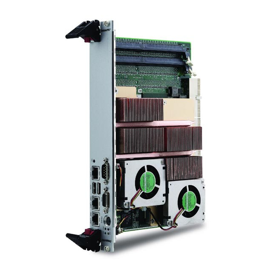
Summary of Contents for ADLINK Technology cPCI-6860A Series
- Page 1 Series 6U CompactPCI Dual Xeon and Rear I/O Transition Module User’s Guide Recycled Paper...
- Page 3 © Copyright 2005 ADLINK Technology Inc. All Rights Reserved. Manual Rev. 1.30: May 24, 2005 Part No. 50-15028-1020 The information in this document is subject to change without prior notice in order to improve reliability, design and function and does not represent a commitment on the part of the manufacturer.
- Page 4 Getting service from ADLINK Customer Satisfaction is top priority for ADLINK Tech Inc. If you need any help or service, please contact us. ADLINK Technology Inc. Web Site http://www.adlinktech.com Sales & Service Service@adlinktech.com +886-2-82265877 +886-2-82265717 Address 9F, No. 166, Jian Yi Road, Chungho City, Taipei, 235 Taiwan.
-
Page 5: Table Of Contents
Table of Contents List of Tables....................iii List of Figures .....................iv Introduction....................1 1.1 Checklist ....................2 cPCI-6860A Front Board ................2 cPCI-R6860A RTM .................2 1.3 Features ....................3 1.4 Specifications..................3 cPCI-6860A front board ................3 cPCI-R6860A RTM .................6 cPCI-6860A and RTM Common Specifications ........7 I/O Connectivity ..................9 1.5 Block Diagram ..................10 Jumpers and Connectors................11... - Page 6 Ultra 320 SCSI..................22 FDD Interface ..................23 40-pin IDE Port ..................23 44-pin IDE Port ..................24 2.6 Jumpers and Switches on the RTM ............25 Primary IDE Jumper Setting on RTM............25 GbE Connection Selection..............25 VGA Connection Selection ..............26 Getting Started...................27 3.1 CPU Installation ..................27 Single CPU Installation .................27 Dual CPU Installation................28 3.2 Baseboard Management Controller Installation ........28...
-
Page 7: List Of Tables
List of Tables Table 1: I/O Connectivity Table ..............9 Table 2: Serial Port COM1 on faceplate..........13 Table 3: VGA Connector on faceplate..........13 Table 4: General Purpose LED definitions ...........14 Table 5: Keyboard/Mouse Combo Connector on faceplate ....14 Table 6: 10/100 Fast Ethernet Connector LAN1 on faceplate ....14 Table 7: LED indicators on the Fast Ethernet port........15 Table 8:... - Page 8 List of Figures Figure 1: Block Diagram ................10 Figure 2: Top View of cPCI-6860A ............12 Figure 3: Front View of cPCI-6860A ............13 Figure 4: Top View of the cPCI-R6860A..........20 Figure 5: cPCI-R6860A Rear View ............20 Figure 6: Location of CN3 for setting the Primary IDE channel .....25 Figure 7: Single CPU Installation............28 Figure 8:...
-
Page 9: Introduction
Introduction This manual provides information on the ADLINK cPCI-6860A Series Single Board Computer (SBC) and its corresponding Rear I/O Transition Module (RTM) cPCI-R6860A. The cPCI-6860A Series products comply with PICMG 2.0 Rev. 3.0 CompactPCI specifications for 6U 2-slot (8 TE/HP) form factor boards. -
Page 10: Checklist
1.1 Checklist The cPCI-6860A Series product supports both front and rear panel I/O. The front board and the cPCI-R6860A RTM are sold separately. The board can be configured with either a single or dual CPU. CPU frequency is specified when the order is placed, therefore the thermal solution (heat sink with fans) is dependent on the configuration. -
Page 11: Features
1.3 Features • Supports single or dual Low Voltage Xeon 1.6GHz, 2.0GHz; or single Xeon 2.0GHz, 2.4GHz; or higher frequency forward compatible CPUs • Compliant with CompactPCI specifications, including PICMG 2.0 R3.0, PICMG 2.1 R1.0, PICMG 2.16 R1.0, and optional PICMG 2.9 R1.0 •... - Page 12 • ® Supports single Intel Xeon 1.8GHz, 2.0GHz, 2.2GHz, 2.4GHz, 2.8GHz with 512KB L2 cache and 400 MHz FSB • ® Supports single Intel Xeon 2.0GHz, 2.8GHz, 3.06GHz with 512KB L2 cache and 533 MHz FSB Chipset • ® Intel E7501 Memory Control Hub (MCH) •...
- Page 13 • IEEE802.3x compliant flow control, support auto-negotiation and link setup • The GbE can be either front access or rear access selectable by onboard switch • PICMG 2.16 PSB when configured for rear access • Speed and connect LEDs on the front panel •...
-
Page 14: Cpci-R6860A Rtm
• W82782D built-in monitoring CPU temperatures, FAN speed, system temperature, V core, and DC voltages. • Watchdog timer: Programmable I/O port on addresses 02Eh and 02FH. Programmable timer for 1 to 255 seconds or 1 to 255 minutes. Easy-programming libraries for DOS, Windows 95/98/NT are available. Optional Baseboard Management Controller (BMC) •... -
Page 15: Cpci-6860A And Rtm Common Specifications
• Supports 1000Base-T, 100Base-TX, and 10Base-T (IEEE 802.3, 802.3u, and 802.3ab) • Provides two additional RJ-45 connectors for the GbE ports on the cPCI-6860A front board SCSI • Wide Ultra320 SCSI interface with synchronous transfer rate of up to 320MBps on a LVD SCSI bus •... - Page 16 Note: Certified with ADLINK thermal design. The thermal performance is dependent on the cooling design. Forced air-cooling with 50 CFM is required for both single 2.4G Xeon or dual low-voltage 1.6G Xeon configurations. The temperature limit of optional mass storage devices can impact the thermal specification of the board.
-
Page 17: I/O Connectivity
I/O Connectivity cPCI-6860A RTM (cPCI-R6860A) Faceplate Faceplate Board Serial Port (COM1) Y (DB-9) Serial Port (COM2) Y (J3, DB-9) Serial Port (MGMT) Y (J4, DB-9) PS2 Keyboard Y (J3, PS2) Y (PS2) PS2 Mouse Y (J3, PS2) Y (DB-15) Y (DB-15) USB A (port 1, port 2) Y (dual USB) Y (J3/J4, dual... -
Page 18: Block Diagram
1.5 Block Diagram CPU 1 CPU 0 Clock Gen LP Xeon LP Xeon ICS932S203 Or Xeon cPCI-6860A 100/133 MHz x4 REG-DDR w/ECC 2 x 2GB Max 100/133 MHz 2x E7501 2 channels HI-B P64H2 144 bits REG-DDR w/ECC 2 x 2GB Max HI-C HI V2.0... -
Page 19: Jumpers And Connectors
Jumpers and Connectors This chapter provides information about the SBC and RTM board layout, connector definitions, and jumper settings. It includes information on the following: • cPCI-6860A Board Outline & Front View • cPCI-6860A Connector Pin Assignments • cPCI-R6860A Board Outline & Rear View •... -
Page 20: Cpci-6860A Board Outline & Front View
2.1 cPCI-6860A Board Outline & Front View cPCI-6860A Top View DIMM 0 DIMM 1 Battery CompactPCI CPU 1 Connectors J1 ~ J4 CPU 0 Figure 2: Top View of cPCI-6860A 12 •Jumpers and Connectors... -
Page 21: Cpci-6860A Front View
cPCI-6860A Front View Figure 3: Front View of cPCI-6860A 2.2 cPCI-6860A Connectors Pin Assignment Serial Port COM1 Connector Signal Name DCD, Data carrier detect RXD, Receive data TXD, Transmit data DTR, Data terminal ready GND, ground DSR, Data set ready RTS, Request to send CTS, Clear to send RI, Ring indicator... -
Page 22: General Purpose Led Definitions
General Purpose LED definitions Color Status Description IDE Media IDE idle Access IDE access System is not power-on or power failed Power OK Green Power ON WDT is not enable Watchdog timer Yellow WDT Time out status Blinking WDT is enable System is powered OFF and can be Hot-swap Blue... -
Page 23: Gigabit Ethernet Ports
Color Status Description 10Mbps transfer rate Link Speed LED Amber 100Mbps transfer rate No link Link / Activity LED Green Connecting Blinking Active/Data transferring Table 7: LED indicators on the Fast Ethernet port Gigabit Ethernet Ports Signal Name MDI0+ 1 2 3 4 5 6 7 8 MDI0- MDI1+ MDI2+... -
Page 24: Compactpci J1 Pin Assignments
CompactPCI J1 Pin Assignments REQ64# ENUM# +3.3V S1AD[1] V(I/O) S1AD[0] ACK64# +3.3V S1AD[4] S1AD[3] S1AD[2] S1AD[7] +3.3V S1AD[6] AD[5] +3.3V S1AD[9] S1AD[8] M66EN S1C/BE[0]# GND S1AD[12] V(I/O) S1AD[11] S1AD[10] +3.3V S1AD[15] S1AD[14] S1AD[13] S1SERR# +3.3V S1PAR S1C/BE[1]# GND +3.3V IPMB_SCL IPMB_SDA S1PERR# GND GND S1DEVSEL#... -
Page 25: Compact Pci J2 Pin Assignment
Compact PCI J2 Pin Assignment Table 12: CompactPCI J2 pin assignments Note: These signals are not connected. These signals are pulled high on the board. Jumpers and Connectors • 17... -
Page 26: Compactpci J3 Pin Assignments
CompactPCI J3 Pin Assignments LPa_DA+ LPa_DA- LPa_DC+ LPa_DC- LPa_DB+ LPa_DB- LPa_DD+ LPa_DD- LPb_DA+ LPb_DA- LPb_DC+ LPb_DC- LPb_DB+ LPb_DB- LPb_DD+ LPb_DD- PDACT# PDCS1# PDCS3# PDA0 PDA2 PPDIAG LILED#_B PDIRQ14 PDA1 PDDACK# PDDREQ PDIOW# PDIORDY PDIOR# PDD13 PDD1 PDD14 PDD0 PDD15 PDD4 PDD11 PDD3 PDD12... -
Page 27: Compactpci J4 Pin Assignments
CompactPCI J4 Pin Assignments CLK66 HI21 GND 100LED#_B 1000LED#_A GND PSTBF PSTBS HI20 HI15 HI14 HI13 HI12 HI11 GND 100LED#_A HI10 PUSTBF PUSTBS 3.3V 3.3V 3.3V 3.3V 3.3V HI16 HI17 HI18 12-14 GND RIO_RST# SDA0 SDA1 SDA2 SDDRQ SDACK# SDD0 SDD1 SDD2 SDD3... -
Page 28: Cpci-R6860A Rtm Board Outline & Rear View
2.4 cPCI-R6860A RTM Board Outline & Rear View cPCI-R6860A Board Outline and Rear View CompactPCI rJ3, rJ4 34pin 40-pin Secondary IDE 40-pin Primary IDE SCSI Primary IDE Primary IDE 44-pin for 2.5 CF Socket inches HDD Figure 4: Top View of the cPCI-R6860A cPCI-R6860A Rear View Figure 5: cPCI-R6860A Rear View... -
Page 29: Cpci-R6860A Connectors & Pin Assignments
2.5 cPCI-R6860A Connectors & Pin Assignments Connectors on the RTM with the same functionality as the cPCI-6860A and having the same pin definition will not be highlighted in the following section. Below is a list of common front and rear interfaces with the same pin definitions. Please refer to the relevant section for further detail. -
Page 30: Ultra 320 Scsi
Ultra 320 SCSI Signal Signal LVDP12 LVDM12 LVDP13 LVDM13 LVDP14 LVDM14 LVDP15 LVDM15 LVDPHP LVDPHM LVDP0 LVDM0 LVDP1 LVDM1 LVDP2 LVDM2 LVDP3 LVDM3 LVDP4 LVDM4 LVDP5 LVDM5 LVDP6 LVDM6 LVDP7 LVDM7 LVDPLP LVDPLM GROUND GROUND DFFSENSE LVEXT68 LVTRMPWR LVTRMPWR LVTRMPWR LVTRMPWR N.C. -
Page 31: Fdd Interface
FDD Interface Signal Signal Ground DRVDEN0 Ground DRVDEN1 Ground INDEX# Ground MTR0# Ground DS1# Ground DS0# Ground MTR1# Ground FDIR# Ground STEP# Ground WDATA# Ground WGATE# Ground TRACK0# Ground WPT# Ground RDATA# Ground HDSEL# Ground DSKCHG# Table 18: FDD Interaface on RTM 40-pin IDE Port Signal Signal... -
Page 32: 44-Pin Ide Port
44-pin IDE Port Signal Signal RESET- Ground DD10 DD11 DD12 DD13 DD14 DD15 Ground N.C (key pin) DMARQ Ground DIOW- Ground DIOR- Ground IORDY CSEL DMACK- Ground INTRQ Reserved PDIAG- CS0- CS1- DASP- Ground Ground TYPE- Table 20: 44-pin Primary IDE pin-header (CN8) on RTM 24 •Jumpers and Connectors... -
Page 33: Jumpers And Switches On The Rtm
2.6 Jumpers and Switches on the RTM Primary IDE Jumper Setting on RTM compact flash card socket on the RTM can either be set to master or slave. Jumper CN3 to the left of the CF card socket is used to set the Primary IDE channel. -
Page 34: Vga Connection Selection
SW1, SW3: LAN2 Connecting Selection Switch Switch LAN 2 Connecting State State S1-1 S3-1 S1-2 S3-2 PICMG 2.16 Backplane S1-3 S3-3 S1-4 S3-4 S1-1 S3-1 S1-2 S3-2 Rear Panel (Default) S1-3 S3-3 S1-4 S3-4 Table 22: LAN2 Connecting Selection VGA Connection Selection The cPCI-6860A supports dual CRT output on front and rear I/O. -
Page 35: Getting Started
Getting Started This chapter provides information on how to install peripherals onto the cPCI-6860A and cPCI-R6860A RTM. Topics covered include: • CPU Installation • Board Management Controller Installation • Thermal Module Installation • Memory Installation • HDD Installation • CF Installation •... -
Page 36: Dual Cpu Installation
CAUTION: DO NOT install the single CPU configuration with the CPU in the CPU0 Socket. This is an invalid configuration and the board will not operate Install CPU here for single CPU configuration Figure 7: Single CPU Installation Dual CPU Installation When using dual CPU configuration, ensure that the identical Low-Voltage Xeon CPU models are used. -
Page 37: Figure 8: Bmc Card Installation
To install the BMC, align the connector on the underside of the BMC card with the socket on the cPCI-6860A as shown below in Figure 8. Use the cut-out on the BMC card and the thermal module mounting hole as a visual aid. Press down on the card to ensure it is fully inserted into the socket. -
Page 38: Thermal Module Installation
3.3 Thermal Module Installation Before installing the thermal module (heat sink), ensure that the CPU(s) is completely seated in the CPU socket and the locking lever of the CPU socket is locked. If the product comes with the thermal module installed, skip this section. -
Page 39: Figure 10: Install O-Rings Onto Thermal Module
components on the board during thermal module installation and to firmly secure the BMC card (if installed) Figure 10: Install O-rings onto Thermal Module Carefully install the thermal module onto the board (see orientation shown in Figure 9), ensuring that the thermal pads are in contact with the board components. -
Page 40: Figure 11: Install Thermal Module Onto Sbc
Figure 11: Install Thermal Module onto SBC After installing the thermal module, connect the fan power cables to the onboard fan connectors as shown and secure the cables to the thermal module using the provided tie-straps to prevent them from catching during insertion or removal of the SBC. -
Page 41: Memory Installation
3.4 Memory Installation The cPCI-6860A SBC supports 144-bit wide registered DDR, which is provided using two 72-bit ECC DIMM sockets. The maximum memory capacity is 4GB. If memory is pre-installed with the product package, this section may be skipped. The memory must be installed in pairs, that is, TWO identical memory modules (in size as well as in capacity) installed in the two DIMM sockets. - Page 42 A 2.5 inch HDD can either be installed on the cPCI-R6860A RTM or in the chassis. If a HDD comes pre-installed with the cPCI-R6860A product package, skip this section. Step 1: Loosen the four screws that hold the HDD mounting bracket in place from the bottom side of the RTM and remove the bracket from the RTM (see photo below).
- Page 43 44 pin IDE Cable Screw Screw Step 3: Mount the HDD bracket in its original location on the RTM using the four screws removed in Step 1 (see diagrams below). 44 pin IDE Bracket Socket Bracket Bracket Bracket Getting Started • 35...
-
Page 44: Cf Installation
44 pin IDE Cable Screw Screw Screw Screw Note A: The IDE cable should be folded away as shown in the above drawing and away from obstruction during insertion and extraction of the board from its slot. 3.6 CF Installation A standard CompactFlash (CF) card has an ATA interface that is fully compatible with that of the IDE HDD. -
Page 45: Note For Adlink 6400 Series Subsystems
Note for ADLINK 6400 Series Subsystems When installing (or removing) the cPCI-R6860A RTM in (from) an ADLINK 6400 Series Subsystem, first demount the chassis from the rack (if mounted) and remove the top cover of the chassis. Push or pull the cabling as required to prevent damage occurring while carefully and gently inserting or removing the RTM. -
Page 47: Device Driver Installation
Device Driver Installation 4.1 Intel® E7501 Chipset This section describes the installation procedure for the Intel® E7501 chipset device driver under Windows 2000 and Windows XP. System Requirements One of the following operating systems must be fully installed on the system before installing any other driver, utilities, or software: ®... -
Page 48: Driver Installation Under Windows 2000
4.2 Driver Installation Under Windows 2000 This section describes installation procedures for all software drivers under Windows 2000. Please follow the instructions carefully to ensure efficiency. VGA Driver Installation This section describes how to install the ATI 3D Rage XL VGA driver that comes with the ADLINK CD. -
Page 49: Scsi Driver Installation
SCSI driver Installation This section describes the SCSI driver installation for the SCSI controller LSI (SYMBIOS) 53C1000R for the optional RTM. All related drivers are stored in the ADLINK CD under the directory: x:\cPCI\cPCI-6860A\SCSI\53C1020-U320\Win2000, where x: is the location of the CD-ROM drive. The 53C1020 driver in the ADLINK CD only supports the Windows 2000 environment. -
Page 50: Lan Driver Installation
LAN Driver Installation This section describes the LAN driver installation process for the Intel® 82562EM and 82546EB Gigabit Ethernet controller under Windows XP. The Intel® software utilities package include Diagnostics utility, Makedisk utility, and 10/100/1000Mbps Ethernet device drivers. All drivers and utilities are stored ADLINK under... - Page 51 During Windows 2000 installation, a SCSI driver will be automatically installed. It is recommended that the user manually updates to the most updated driver, which is shipped with the ADLINK CD to ensure total compatibility. After Windows 2000 installation is completed, update to the new driver by following the steps below: Boot up Windows 2000.
-
Page 52: Appendix
Appendix IPMI Function List The following table lists the IPMI V1.0 functions supported by the cPCI-6860A. IPMI V1.0 Function List cPCI-6860A IPM Device “Global” Commands Get Device ID Cold Reset Warm Reset Get Self Test Results Set ACPI Power State Get ACPI Power State Get Device GUID BMC Watchdog Timer Commands... - Page 53 Event Commands Set Event Receiver Get Event Receiver Platform Event (a.k.a. “Event Message”) Sensor Device Commands Get Device SDR Info Get Device SDR Reserve Device SDR Repository Get Sensor Reading Factors Set Sensor Hysteresis Get Sensor Hysteresis Set Sensor Threshold Get Sensor Threshold Set Sensor Event Enable Get Sensor Event Enable...
- Page 54 SEL Device Commands Get SEL Info Get SEL Allocation Info Reserve SEL Get SEL Entry Add SEL Entry Partial Add SEL Entry Delete SEL Entry Clear SEL Get SEL Time Set SEL Time Note 1: SEL storage is not supported in random access Note 2: SDR information is read only.
-
Page 55: Warranty Policy
Warranty Policy Thank you for choosing ADLINK. To understand your rights and enjoy all the after-sales services we offer, please read the following carefully. Before using ADLINK’s products please read the user manual and follow the instructions exactly. When sending in damaged products for repair, please attach an RMA application form which can be downloaded from: http://rma.adlinktech.com/policy/. - Page 56 • Damage from improper repair unauthorized ADLINK technicians. • Products with altered and/or damaged serial numbers are not entitled to our service. • This warranty is not transferable or extendible. • Other categories not protected under our warranty. Customers are responsible for all fees necessary to transport damaged products to ADLINK.
Need help?
Do you have a question about the cPCI-6860A Series and is the answer not in the manual?
Questions and answers