Table of Contents

Subscribe to Our Youtube Channel
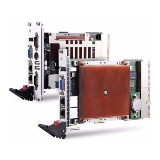
Related Manuals for ADLINK Technology cPCI-3920 Series


Summary of Contents for ADLINK Technology cPCI-3920 Series
- Page 1 Series 3U CompactPCI Single Board Computer with Intel® Core™ 2 Duo, Core™ Duo, Celeron® M Processor User’s Manual 2.00 Manual Rev. May 30, 2008 Revision Date: 50-15064-1000 Part No: Advance Technologies; Automate the World.
-
Page 2: Revision History
Revision History Revision Release Date Description of Change(s) 2.00 2008/05/30 Initial Release... - Page 3 Copyright 2008 ADLINK TECHNOLOGY INC. All Rights Reserved. The information in this document is subject to change without prior notice in order to improve reliability, design, and function and does not represent a commitment on the part of the manufacturer.
- Page 4 Getting Service from ADLINK Customer Satisfaction is top priority for ADLINK Technology Inc. Please contact us should you require any service or assistance. ADLINK TECHNOLOGY INC. Web Site: http://www.adlinktech.com Sales & Service: Service@adlinktech.com TEL: +886-2-82265877 FAX: +886-2-82265717 Address: 9F, No. 166, Jian Yi Road, Chungho City,...
-
Page 5: Table Of Contents
Table of Contents Table of Contents..............i List of Tables................v List of Figures ................ vi 1 Overview ................1 Introduction ................1 Features................2 Block Diagram ..............3 Product List................4 SBC ................4 Rear Transition Module ..........4 Accessories .............. - Page 6 Supported Processors, Maximum Power Dissipation ... 23 Memory ................. 24 Intel® 3100 Chipset Overview ........24 Volari™ Z11 Graphics Controller ........26 Peripherals................. 28 Timer ................28 Watchdog Timer ............28 Battery ................29 Reset ................29 SMBus Devices ............30 Thermal Management/ System Monitoring ....
- Page 7 7 BIOS Setup Utility............. 67 Starting the BIOS............... 67 Setup Menu ..............68 Navigation ..............68 Hotkey Descriptions ............70 Main Setup................. 71 System Time/System Date ........... 71 Advanced BIOS Setup............72 CPU Configuration ............73 IDE Configuration ............74 AHCI Configuration ............
- Page 8 This page intentionally left blank. Table of Contents...
-
Page 9: List Of Tables
List of Tables Table 2-1: I/O Connectivity ............10 Table 2-2: Power consumption of Core™ 2 Duo LV (L7400) .. 11 Table 2-3: Power consumption of Core™ 2 Duo LV (U2500) .. 12 Table 2-4: Power consumption of Celeron M LV(423) ..... 13 Table 3-1: Supported Processors, Power Dissipation ..... - Page 10 List of Figures Figure 1-1: cPCI-3920 Block Diagram ......... 3 Figure 2-1: cPCI-3920 Mechanical Dimensions......14 Figure 2-2: cPCI-R3920 Mechanical Dimensions ...... 15 Figure 2-3: cPCI-3920 Board Layout ......... 16 Figure 2-4: cPCI-3920A Assembly and Front Panel ....17 Figure 2-5: DB-3920L2 Daughter Board Layout ......18 Figure 2-6: cPCI-3920B Assembly and Front Panel ....
-
Page 11: Overview
Overview 1.1 Introduction The cPCI-3920 is a highly integrated 3U CompactPCI SBC in sin- gle slot (4HP) or dual slot (8HP) width form factor. It has been designed to support Intel® lower power Core™ 2 Duo, Core™ Duo and Celeron® M processors in FC-BGA package with a range of 1.0GHz to 1.5GHz at FSB 533MHz to 667MHz. -
Page 12: Features
1.2 Features 3U CompactPCI SBC in 4HP or 8HP width form factor Low power Intel Core 2 Duo 1.5GHz, Core™ Duo 1.2GHz, Celeron® M 1.0GHz processors Intel® 3100 chipset (Memory and I/O Hub integrated chip) Single channel DDR2 registered and ECC memory at 400MHz Two PCI-Express Gigabit Ethernet ports in the front or RTM Support USB 2.0 NAND flash module, up to 8GB... -
Page 13: Block Diagram
1.3 Block Diagram Intel® Core 2 Duo (Merom) GbE 1/2 USB 3 USB x2 GbE 1/2 82571EB PCI-E PCI-E x4 (1x) or x1 (4x) COM 1/2 USB 2 SATA (3x) SMbus USB 1 Intel® 3100 W83792AG Chipset (Whitmore Lake) COM 3/4 F8126 pin header USB 0... -
Page 14: Product List
1.4 Product List Products included in the cPCI-3920 Series include: cPCI-3920A: single-slot (4HP) width 3U CompactPCI fea- turing Intel LV Core 2 Duo 1.5GHz, Core Duo 1.2GHz or ULV Celeron 1.0GHz processors; 512MB, 1GB or 2GB onboard memory; optional USB flash disk module cPCI-3920B: dual-slot(8HP) width 3U CompactPCI featur- ing Intel LV Core 2 Duo 1.5GHz, Core Duo 1.2GHz or ULV... -
Page 15: Package Contents
ADLINK. The packing contents of the cPCI-3600 Series are non-standard configurations and may vary depending on customer requests. CPU module The cPCI-3920 Series CPU Module CPU, RAM, and HDD specifications will differ depending on options selected Thermal module is assembled on the board... - Page 16 This page intentionally left blank. Overview...
-
Page 17: Specifications
Specifications 2.1 CPU, memory, and chipset ™ uFC-BGA Intel® Core 2 Duo LV (L7400) 1.5 GHz, FSB 667MHz, 4 MB L2 cache ™ uFC-BGA Intel Intel® Core Duo ULV (U2500) 1.2 GHz, Processor FSB 533MHz, 2 MB L2 cache uFC-BGA Intel Intel® Celeron® M ULV (423) 1.06 GHz, FSB 533MHz, 1 MB L2 cache Intel®... - Page 18 4x serial ports Two DB-9 ports on the front panel, one RS-232 and one RS-232/422/485/485+ (8HP only) Serial Port Two ports are routed to RTM with one DB-9 port on rear panel and one pin header onboard 4x Serial ATA channels: One SATA connector onboard, 2.5”...
-
Page 19: Software
2.3 Software AMI 16Mbit FWH BIOS Microsoft® Windows® XP Professional Microsoft® Windows® Server 2003 Microsoft® Windows® Vista Enterprise, 32-bit version Supported OS RedHat Fedora Core 8 Contact ADLINK for other OS availability 2.4 Mechanical cPCI-3920: 3U 4HP/8HP CompactPCI Form factor cPCI-R3920(T): 3U 4HP CompactPCI cPCI-3920: 100mmx 160mm (LxW) cPCI-R3920: 100mm x 50mm (LxW) -
Page 20: I/O Connectivity Table
2.6 I/O Connectivity Table cPCI-3920A cPCI-3920B cPCI-R3920(T) Faceplate Board Faceplate Board Faceplate Y x2 Y x2 Y (9-pin) Y x3 Y (9-pin) Y (DB-9) (DB-9) x2 (10-pin) Y x3 SATA (7-pin) PS/2 KB/MS Y x3 Y x3 Reset Button Table 2-1: I/O Connectivity Specifications... -
Page 21: Power Consumption
2.7 Power Consumption This section provides the information on the power consumption of cPCI-3920.Power consumption of Intel® Pentium® M Processor: Intel® Core™ 2 Duo LV (L7400) 1.5GHz, FSB 667MHz, 4MB L2 cache Function Configuration Memory DDR2 400 1GB SATA Hard Drive External 3.5”HDD Backplane ADLINK cBP-3208R Rev.B2 Power Supply... -
Page 22: Table 2-3: Power Consumption Of Core™ 2 Duo Lv (U2500)
Processor: Intel® Core™ Duo (U2500) 1.2GHz, FSB 533MHz, 2MB L2 cache Function Configuration Memory DDR2 400 1GB SATA Hard Drive External 3.5”HDD Backplane ADLINK cBP-3208R Rev.B2 Power Supply ZIPPY HG2-6350P 350W Power requirement +3.3V Total Current (A) 1.51 3.274 Watts (W) 4.983 16.37 21.353... -
Page 23: Table 2-4: Power Consumption Of Celeron M Lv(423)
Processor: Intel® Celeron M LV(423) 1.07GHz, FSB 533MHz, 1MB L2 cache Function Configuration Memory DDR2 400 1GB SATA Hard Drive External 3.5”HDD Backplane ADLINK cBP-3208R Rev.B2 Power Supply ZIPPY HG2-6350P 350W Power requirement +3.3V Total Current (A) 1.51 3.274 Watts (W) 4.983 16.37 21.353... -
Page 24: Mechanical Dimensions
2.8 Mechanical Dimensions cPCI-3920A cPCI-3920B Figure 2-1: cPCI-3920 Mechanical Dimensions Specifications... -
Page 25: Cpci-R3920
cPCI-R3920 cPCI-R3920T Figure 2-2: cPCI-R3920 Mechanical Dimensions Specifications... -
Page 26: Board Layout
2.9 Board Layout cPCI-3920 Board Layout U6 Processor CN2 USB port U7 Chipset CN3 VGA port U5 Transformer CN7 Ethernet port U15 Graphics controller CN8 Ethernet port DB-3920L2 daughter U19 Ethernet controller board connector U25 SDRAM CN5 USB pin header CompactPCI J1 CompactPCI J2 connector... -
Page 27: Figure 2-4: Cpci-3920A Assembly And Front Panel
cPCI-3920A Assembly Outline USB flash Thermal Module disk (optional) Battery cPCI-3920A Front Panel Speed ACT Figure 2-4: cPCI-3920A Assembly and Front Panel Reset Button Temperature LED Hot (red): CPU Overtemperature Status, connected to the CPU signal PROCHOT Status LEDs WDT (yellow): Watchdog Status PWR (green): Power Supply Status Gigabit Ethernet LEDs SPEED ON (green): 1000Mbps... -
Page 28: Figure 2-5: Db-3920L2 Daughter Board Layout
DB-3920L2 Daughter Board Components Layout The DB-3920L2 Daughter Board extends the cPCI-3920 from 4HP (cPCI-3920A) to 8HP (cPCI-3920B) version. This addi- tional capability opens up the broadest range of expansion pos- sibilities. The DB-3920L2 module has been designed to include two COM ports, a PS/2 keyboard and mouse port, two USB 2.0 interfaces and a 2.5”... -
Page 29: Figure 2-6: Cpci-3920B Assembly And Front Panel
cPCI-3920B Assembly Outline 2.5” SATA hard drive cPCI-3920B Front Panel Figure 2-6: cPCI-3920B Assembly and Front Panel Specifications... -
Page 30: Figure 2-7: Cpci-R3920(T) Board Layout And Front Panel
Board Layout The cPCI-3920 Series offer two version rear transition modules with the same functionality but different dimensions. The cPCI- R3920 is designed with a 50mm width and the cPCI-R3920T is designed with a 80mm width CN1-R CN1-R CN2-R... -
Page 31: Functional Description
Functional Description The following sections describe the cPCI-3920 main functions and board interfaces. 3.1 CPU, Memory and Chipset CPU: Intel® Core™ Duo and Intel® Core™2 Duo The cPCI-3920 supports the latest Intel® Core™ Duo and Intel® Core™2 Duo processor family up to speeds of 1.5 GHz with up to 667 MHz FSB. -
Page 32: Intel® Celeron® M
The following list sets out some of the key features of the Intel® Core™ Duo and the Intel® Core™2 Duo processors: Two mobile execution cores in one single processor Support of Intel’s Virtualization Technology (Vanderpool) Support of Intel Architecture with Dynamic Execution Outstanding dual-core performance with low power con- sumption On die, primary 32 KB instruction cache and 32KB write-... -
Page 33: Supported Processors, Maximum Power Dissipation
agement that reduce the number of micro-ops handled by the processor. On-die, primary 32-kB instruction cache and 32-kB, write- back, data cache On-die, 1 MB second level cache with Advanced Transfer Cache architecture Advanced branch prediction and data prefetch logic Streaming SIMD extensions 2 (SSE2) that enables break- through levels of performance in multimedia applications including 3D graphics, video decoding/encoding, and... -
Page 34: Memory
Memory The cPCI-3920 supports a single soldered channel DDR2 memory with Error Checking and Correcting (ECC) running at 400 MHz The available memory module configuration is 1 GB. 2 GB avail- able on request, please contact your ADLINK representative. Memory configuration changes are only permitted to be per- Note: formed at the factory. - Page 35 PCI Express The Intel 3100 Chipset provides one configurable x8 PCI Express interface with a maximum theoretical bandwidth of 4 GByte/s. The x8 PCI Express interface may alternatively be configured as two independent x4 PCI Express interfaces with a maximum theoretical bandwidth of 2 GBytes/s each. The Intel®...
-
Page 36: Volari™ Z11 Graphics Controller
System TCO Reduction Circuits SMBus Watchdog Timers PCI 2.3 Interface Two fully functional serial ports 38 General Purpose I/Os (GPIO) IMCH The Intel® 3100 Chipset provides an integrated memory con- troller for direct-connection to one channel of DDR2-400 (unstacked) registered memory devices with ECC. Peak theo- retical memory data bandwidth using DDR2-400 is 3.2 GByte/s Volari™... - Page 37 Supports DDR-II SDRAM memory 32 MB memory configuration Supports VGA BIOS auto memory size detection High Performance Flat Panel Display Interface Supports graphics mode up to 1600x1200@70Hz 16M colors High Integration Built-in CRT FIFO to support ultra high resolution graph- ics modes and reduce CPU wait-state Built-in programmable 24-bit true-color RAMDAC with 230 MHz pixel clock...
-
Page 38: Peripherals
3.2 Peripherals The following standard peripherals are available on the cPCI-3920 board: Timer The cPCI-3920 is equipped with the following timers: Real-Time Clock The IICH contains real-time clock with 256-byte of battery- backed RAM. The real-time clock performs timekeeping functions and includes 256 bytes of general purpose battery-backed CMOS RAM. -
Page 39: Battery
Battery The cPCI-3920 is provided with a 3.0 V “coin cell” lithium battery for the RTC. To replace the battery, proceed as follows: Turn off power Remove the battery Place the new battery in the socket. Make sure that you insert the battery the right way round. The plus pole must be on the top! The lithium battery must be replaced with an identical battery or a battery type recommended by the manufacturer. -
Page 40: Smbus Devices
A reset will be generated by the following conditions: +5 V supply falls below 4.1 V (typ.) +3.3 V supply falls below 2.93 V (typ.) Pushbutton ´RESET" pressed (only on 8HP) Watchdog overflow CompactPCI backplane PRST# input (CompactPCI con- nector J2, pin C17) SMBus Devices The cPCI-3920 provides a System Management Bus (SMBus) for access to several system monitoring and configuration... -
Page 41: Fwh Flash Memory
temperature is too high, the sensor automatically reduces the CPU clock frequency, depending on the mode chosen in the BIOS set- tings. FWH Flash Memory For simple BIOS updating a standard onboard 16 Mbit Firmware Hub device is used. The FWH stores both the system BIOS and graphics BIOS. -
Page 42: Board Interfaces
3.3 Board Interfaces USB Interfaces The cPCI-3920 supports six USB 2.0 ports: one front I/O two front I/O on DB-3920L2 module one onboard to connect a Flash disk two on the Rear I/O module. On the USB 2.0 front panel port, USB cable with up to 5 meters in length can be used. -
Page 43: Table 3-5: Onboard Usb Connector Pin Definition
Onboard USB Connector (CN5) The onboard USB device (CN5 connector) is used to connect a USB Flash Disk. The following figure and table provide pinout information for the onboard USB connector CN5: Signal Function Uv0- Differential USB- Uv0+ Differential USB+ Not connected Not used Not used... - Page 44 USB Flash Disk Mechanical Layout Maximum space reserved for USB flash disk is 50mm x 30mm (LxW) The distance between the centers of connector and screw hole is 27.3mm~27.9mm Maximum allowable connector height is 9.78mm (under 4HP) Figure 3-2: USB Flash Disk Mechanical Layout Functional Description...
-
Page 45: Graphics Controller
Graphics Controller The Volari™ Z11 graphics controller incorporates a powerful 64-bit graphics engine to enhance the performance of 2D operations. The capabilities of the graphics engine include, but are not limited to BitBlt, Color Expansion, Enhanced Color Expansion, Line Draw- ing, Transparent BitBlt, and Rectangle Fill. -
Page 46: Dual Gigabit Ethernet
interface at 250MHz. It can support up to a 1GB/s bandwidth, with a 16-bit DDRII SDRAM interface. A DRAM capacity of 32MB is currently supported on cPCI- 3920 boards. VGA Analog Interface and Connector (CN3) The 15-pin female connector CN3 is used to connect a VGA analog monitor to the cPCI-3920 board. -
Page 47: Table 3-7: Gigabit Connector Cn7/Cn8 Pin Definitions
Gigabit Connector RJ-45 Pin Definitions (CN7/CN8) The CN7/CN8 connector supplies the 10Base-T, 100Base- TX and 1000Base-T interfaces to the Ethernet controller. 10BASE--T 100BASE--TX 1000BASE--T SIGNAL SIGNAL SIGNAL BI_DA+ BI_DA- BI_DB+ BI_DC+ BI_DC- TX-- RX-- BI_DB- BI_DD+ BI_DD- Table 3-7: Gigabit Connector CN7/CN8 Pin Definitions Ethernet LED Status SPEED (green): When green it indicates a 1000BASE-TX connection. -
Page 48: Board-To-Board Connector
remains off, a valid link has not been established due to a miss- ing or a fault connection. Status SPEED LED ACT LED Network link is not established LINK 10/100 Mbps ACTIVE BLINK LINK 1000 Mbps ACTIVE BLINK Table 3-8: Ethernet LED Status Definitions Board-to-Board Connector The Board-to-Board Connector (CN4) connects the main board to the DB-3920L2 daughter board, allowing I/O expansion and HDD... -
Page 49: Table 3-9: Board-To-Board Connector Pin Definition
CN4 Pin Assignment SIGNAL SIGNAL LPC_FRAME# USB3-D- LPC_AD[3] USB3-D+ LPC_AD[2] LPC_AD[1] USB2_D- LPC_AD[0] USB2_D+ PCIRST[4]# CLK33_SIO SATA0_RX- SATA0_RX+ SATA0_TX+ SATA0_TX- +3.3V USB_OC3# +3.3V USB_OCS# B2B_IN# LPC_LDRQ0# KB_CLK A20GATE KB_DAT SERIRQ# MS_CLK KBD_RST# MS_DAT CPU_PWRGD BPM[0]# XDP_DBRESET# BPM[1]# BPM[2]# BPM[3]# TRST# BPM[4]# BPM[5]# CPU_RST#... -
Page 50: Keyboard/ Mouse Interface
Keyboard/ Mouse Interface The keyboard controller is located on the cPCI-3920B and is 8042 software compatible. The PC/AT standard keyboard/mouse connector is a PS/2-type 6- pin shielded Mini-DIN connector. A Y-cable to connect a mouse device and/or a keyboard to the PS/2 connector is included in the package of cPCI-3920B. -
Page 51: Universal Serial Ports
Universal Serial Ports Two PC-compatible serial RS-232, 9-pin D-Sub ports are avail- able and fully compatible with the 16C550 controller. These port includes a complete set of handshaking and modem control sig- nals. Data transfer rates up to 115.2 kB/s are supported. The COM3 interface is routed to the connector CN1. -
Page 52: Table 3-13: Com4 Mode Switch Settings
COM4 Mode Switch Settings Location RS232 Full Modem RS422 Half Duplex RS485 Half Duplex RS485+ Half Duplex Table 3-13: COM4 Mode Switch Settings Functional Description... -
Page 53: Serial Ata Interfaces
Serial ATA Interfaces The cPCI-3920 provides up to four SATA interfaces. Three SATA ports, SATA1, SATA2 and SATA3, can be used only on the Rear Transition Module I/O interface. All SATA ports can be used simul- taneously. SATA PORT CONNECTOR USAGE Onboard 2.5”... -
Page 54: Table 3-14: Sata0 Connector Pin Definition
SATA0 Connector, CN3-2 SIGNAL FUNCTION Signal Segment Key Ground signal SATA_TX2+ Differential Transmit+ SATA_TX2- Differential Transmit- Ground signal SATA_RX2- Differential Receive- SATA_RX2+ Differential Receive+ Ground signal Signal Segment "L" Central Connector Polarizer Power Segment "L" 3.3V 3.3V power 3.3V 3.3V power 3.3V 3.3V power Ground signal... -
Page 55: Compactpci Bus Interfaces
CompactPCI Bus Interfaces The complete CompactPCI connector configuration comprises two connectors named J1 and J2. Their function is as follows: J1: 32-bit CompactPCI interface with PCI bus signals, arbi- tration, clock and power J2: has optional Rear I/O interface functionality or 64-bit ter- mination The board is capable of driving up to seven CompactPCI slots, with individual arbitration and clock signals. -
Page 56: Table 3-15: Compactpci J1 Pin Assignment
CompactPCI J1 Pin Assignment Note: (1) NC = no connect (2) Onboard pull low to GND (3) Onboard pull high to +5V (4) Onboard pull high to +3.3V REQ64# ENUM# +3.3V AD[1] V(I/O) AD[0] ACK64# GND +3.3V AD[4] AD[3] AD[2] AD[7] +3.3V AD[6]... - Page 57 CompactPCI J2 Pin Assignment The cPCI-3920 board provides Rear I/O connectivity for special compact systems. Some standard PC interfaces are imple- mented and assigned to the front panel and to the rear connec- tor J2. When the Rear I/O module is used, the signals of some of the main board/front panel connectors are routed to the Rear I/O module interface.
-
Page 58: Table 3-16: Compactpci J2 Pin Assignment
Legend for J2 Pin Assignment N.C. GA[4] GA[3] GA[2] GA[1] GA[0] N.C. CLK[6] COM1_RXD COM2_RXD GPIO7 N.C. CLK[5] COM1_TXD COM1_TXD GPIO6 N.C. GND/CLK100+ GND/CLK100+ SMB_SDA SMB_SCL SMB_ALERT GND N.C. SATA3_TX+ SATA3_TX- SATA3_RX+ SATA3_RX- N.C. USB4_D+ USB4_D RST_BP# N.C. GNT[6]#pull N.C. USB4_PWR USB5_PWR DEGXB... -
Page 59: Board Interfaces On Rtm
3.4 Board Interfaces on RTM There are two identical USB interfaces on the CPCI-R3920(T) RTM, each with a maximum transfer rate of 480 Mb!s provided for connecting USB devices. One USB peripheral may be connected to each port. To connect more USB devices than there are avail- able ports, an external hub is required. -
Page 60: Com1 And Com2 Interfaces
Gigabit Connector RJ-45 Pin Definitions (CN6-R) The CN7/CN8 connector supplies the 10Base-T, 100Base- TX and 1000Base-T interfaces to the Ethernet controller. 10BASE--T 100BASE--TX 1000BASE--T SIGNAL SIGNAL SIGNAL BI_DA+ BI_DA- BI_DB+ BI_DC+ BI_DC- TX-- RX-- BI_DB- BI_DD+ BI_DD- Table 3-18: RTM Gigabit Connector Pin Definitions The Ethernet transmission can operate effectively using a Note: CAT5 cable or higher specifications. -
Page 61: Serial Ata Interfaces - Sata1-3
COM1 DB-9 Serial Port Connector (CN3-R) Pin # RS-232 not used RXD, Receive data TXD, Transmit data not used GND, Ground not used not used not used not used Table 3-19: COM1 Serial Port Connector Pin Definition COM2 Onboard Serial Port Connector (CN1-R) Pin # RS-232 not used... -
Page 62: Sata1-3 Connectors Cn2-R, Cn4-R And Cn5-R
SATA1-3 Connectors CN2-R, CN4-R and CN5-R Pin # Signal Pin # Signal Table 3-21: SATA1-3 Connectors Pin Definition When using a Serial ATA cable, it is recommended to use a Note: special right-angled Serial ATA cable due to possible space limitations within the system. - Page 63 CompactPCI Connector rJ2 Functional Description...
-
Page 64: Table 3-22: Compactpci Rj2 Pin Assignment
CompactPCI rJ2 Pin Assignment Legend for rJ2 Pin Assignment N.C. GA[4] GA[3] GA[2] GA[1] GA[0] N.C. CLK[6] COM1_RXD COM2_RXD N.C. N.C. CLK[5] COM1_TXD COM1_TXD N.C. N.C. GND/CLK100 GND/CLK100 SMB_SDA SMB_SCL SMB_ALERT N.C. SATA3_TX+ SATA3_TX- SATA3_RX+ SATA3_RX- N.C. USB4_D+ USB4_D RST_BP# N.C. -
Page 65: Getting Started
Getting Started The cPCI-3920 has been designed for easy installation. However, the following standard precautions, installation procedures, and general information must be observed to ensure proper installation and to preclude damage to the board, other system components, or injury to personnel. 4.1 Safety Requirements The following safety precautions must be observed when installing or operating the cPCI-3920. -
Page 66: Installing The Hard Disk Drive
4.2 Installing the Hard Disk Drive The cPCI-3920 supports a slim-type 2.5” SATA HDD. If the cPCI- 3920 comes with a pre-installed HDD, proceed to the next section. To install the hard disk drive: 1. Place the HDD into the bracket as shown. 2. -
Page 67: Installing The Cpci-3920 To The Chassis
RTMs to the chassis as these are shorter than front boards. Refer to previous sections when connecting or installing peripher- als to the RTM. Make sure that the RTMs you are installing are compatible with the cPCI-3920 Series. You must install the correct RTM to enable some functional- Note: ities (I/O interfaces) on the rear panel. -
Page 68: Hot Swap Procedures
4.5 Hot Swap Procedures The cPCI-3920 is not designed for hot swap operation. Do not attempt to hot swap this board. However, the cPCI-3920 supports the addition or removal of other boards whilst in a powered-up state. Getting Started... -
Page 69: Driver Installation
Driver Installation The cPCI-3920 drivers are available from the ADLINK All-In-One CD at X:\cPCI\cPCI-3920\, or from the ADLINK website (http://www.adlinktech.com). The following describes the driver installation procedures for Windows® 2000, Windows® XP or Windows® Server 2003: 1. Install the Windows operating system before installing any driver. - Page 70 This page intentionally left blank. Driver Installation...
-
Page 71: Watchdog Timer
Watchdog Timer 6.1 WDT Overview This section explains the operation of the cPCI-3920’s Watchdog Timer (WDT). The primary function of the WDT is to monitor the cPCI-3920 operation and to reset the system if a software applica- tion fails to function as programmed. The following WDT functions may be controlled using a software application: enabled and disabled reloading timeout value... -
Page 72: Using The Watchdog Timer In An Application
the internal IO to control the WDT and retrieve its status. The basic functions of the WDT include: Setting the watchdog timeout interval Starting the timer countdown Selecting 1 step or 2 step WDT Enabling or disabling WDT Reloading the timeout value to keep the watchdog from tim- ing out Setting the range of the timeout period from 1 µs to 1 sec- ond, or from 1 ms to 1050 seconds... - Page 73 void write_config_data_byte(unsigned char,unsigned char); unsigned char read_config_data_byte(unsigned char); unsigned int read_wdt_io_base(); /* access wdt I/O registers routines */ void write_preload_val2_reg(unsigned long int); void clear_preload_val1_reg(); void unlocking_reg(); /* Global parameter */ unsigned int wdt_io_base; void main(void) unsigned int wdt_io_base; unsigned long int time_out_val=0; wdt_io_base=read_wdt_io_base();...
- Page 74 outportb(wdt_io_base+0x18,2);//watchdog timer enable!! printf("\nPlease waiting for Watch-Dog Timer time-out!!"); /************************************/ unsigned int read_wdt_io_base() unsigned char_wdt_io_base[2]; *p_wdt_io_base; p_wdt_io_base=&_wdt_io_base; enter_config_mode(); write_config_data_byte(0x07,6);//select logic 6 - WDT _wdt_io_base[1]=read_config_data_byte(0x60) _wdt_io_base[0]=read_config_data_byte(0x61) exit_config_mode(); return (*p_wdt_io_base); /************************************/ void enter_config_mode() outportb(config_port_index,0x80); outportb(0xeb,00); //io delay outportb(config_port_index,0x86); /************************************/ void exit_config_mode() outportb(config_port_index,0x68); Watchdog Timer...
- Page 75 outportb(0xeb,00); //io delay outportb(config_port_index,0x08); /************************************/ unsigned char read_config_data_byte(unsigned char _index) unsigned char r_data; outportb(config_port_index,_index); outportb(0xeb,00); //io delay r_data=inportb(config_port_data); return(r_data); /************************************/ void write_config_data_byte(unsigned char _index,unsigned char _data) outportb(config_port_index,_index); outportb(0xeb,00); //io delay outportb(config_port_data,_data); /************************************/ void write_preload_val2_reg(unsigned long int _time_out_val) unsigned char *p_data; "unsigned char"...
- Page 76 unlocking_reg(); outportb(wdt_io_base+5,*p_data); p_data++; printf("%x\n",*p_data); unlocking_reg(); outportb(wdt_io_base+6,*p_data); /************************************/ void clear_preload_val1_reg() unlocking_reg(); outportb(wdt_io_base,0x00); unlocking_reg(); outportb(wdt_io_base+1,0x00); unlocking_reg(); outportb(wdt_io_base+2,0x00); /************************************/ void unlocking_reg() outportb(wdt_io_base+12,0x80); outportb(0xeb,00); //io delay outportb(wdt_io_base+12,0x86); Watchdog Timer...
-
Page 77: Bios Setup Utility
BIOS Setup Utility The following chapter describes basic navigation for the AMIBIOS®8 BIOS setup utility. 7.1 Starting the BIOS To enter the setup screen, follow these steps: 1. Power on the motherboard 2. Press the < Delete > key on your keyboard when you see the following text prompt: <... -
Page 78: Setup Menu
Setup Menu The main BIOS setup menu is the first screen that you can navi- gate. Each main BIOS setup menu option is described in this user’s guide. The Main BIOS setup menu screen has two main frames. The left frame displays all the options that can be configured. - Page 79 These keys include < F1 >, < F10 >, < Enter >, < ESC >, < Arrow > keys, and so on. . There is a hot key legend located in the right frame on most Note: setup screens. The < F8 > key on your keyboard is the Fail-Safe key. It is not dis- played on the key legend by default.
-
Page 80: Hotkey Descriptions
Hotkey Descriptions The < F1 > key allows you to display the General Help screen. Press the < F1 > key to open the General Help screen. The < F10 > key allows you to save any changes you have made and exit Setup. -
Page 81: Main Setup
the < Enter > key to abort this function and return to the pre- vious screen. The < Enter > key allows you to display or change the setup Enter option listed for a particular setup item. The < Enter > key can also allow you to display the setup sub-screens. -
Page 82: Advanced Bios Setup
keys to move between fields. The date must be entered in MM/ DD/YY format. The time is entered in HH:MM:SS format. The time is in 24-hour format. For example, 5:30 A.M. ap- Note: pears as 05:30:00, and 5:30 P.M. as 17:30:00. 7.3 Advanced BIOS Setup Select the Advanced tab from the setup screen to enter the Advanced BIOS Setup screen. -
Page 83: Cpu Configuration
CPU Configuration You can use this screen to select options for the CPU Configura- tion Settings. Use the up and down < Arrow > keys to select an item. Use the < + > and < - > keys to change the value of the selected option. -
Page 84: Ide Configuration
agement. When Disabled, the IVT extensions will be disabled. However, software virtual machine managers like VMware can still be used if virtualization is required. Intel® SpeedStep™ Techology This allows you to enable or disable Intel® SpeedStep™ Tech- nology. IDE Configuration You can use this screen to select options for the IDE Configuration Settings. - Page 85 ATA/IDE Configuration This item specifies whether the IDE channels should be initial- ized in Compatible or Enhanced mode of operation. The set- tings are Disabled, Compatible and Enhanced. Configure SATA as This item specifies SATA channels transport to what kind of channels.
-
Page 86: Ahci Configuration
AHCI Configuration While entering setup BIOS auto detects the presence of IDE devices. USB Configuration You can use this screen to select options for the USB Configura- tion. Use the up and down < Arrow > keys to select an item. Use the <... - Page 87 USB Function Specifies enabled USB host controller. 4 USB ports – set the value to allow 4 USB ports. 2 USB ports – set the value to allow 2 USB ports. Disabled – set the value to deny USB ports. Legacy USB Support Legacy USB Support refers to the USB mouse and USB key- board support.
- Page 88 Enabled Set this value to allow the use of USB devices during boot and while using DOS. This option auto detects USB Keyboards or Mice Auto and if found, allows them to be utilized during boot and while using DOS. Port 64/60 Emulation It uses USB to receive the IO port 64/60 trap to emulate the legacy keyboard controller.
-
Page 89: Hardware Health Configuration
Hardware Health Configuration This option displays the current status of all of the monitored hard- ware devices / components such as voltages and temperatures. BIOS Setup Utility... -
Page 90: Pci/Pnp Setup
7.4 PCI/PnP Setup Select the PCI/PnP tab from the setup screen to enter the Plug and Play BIOS Setup screen. You can display a Plug and Play BIOS Setup option by highlighting it using the < Arrow > keys. The Plug and Play BIOS Setup screen is shown below. -
Page 91: Boot Setup
7.5 Boot Setup Select the Boot tab from the setup screen to enter the Boot BIOS Setup screen. You can select any of the items in the left frame of the screen, such as Boot Device Priority, to go to the sub menu for that item. - Page 92 <Plus> and <Minus> keys to change the value of the selected option. The settings are described on the following pages. The screen is shown below. Quick Boot Disabled – Set this value to allow the BIOS to perform all POST tests. Enabled – Set this value to allow the BIOS to skip certain POST tests to boot faster.
-
Page 93: Boot Device Priority
Boot Device Priority Boot Devices Priority This specifies the boot sequence from the available devices. The 1st Boot Device is primary device. BIOS Setup Utility... -
Page 94: Removable Drives
Removable Drives Removable Drives This specifies the Boot Device Priority sequence from available Removable Drives. Disabled – Set this menu to allow the BIOS to remove device on Boot Device Priority. Device name – Set this menu to allow the BIOS to stay device on Boot Device Pri- ority BIOS Setup Utility... -
Page 95: Security Setup
7.6 Security Setup Password Support Two Levels of Password Protection Provides both a Supervisor and a User password. If you use both passwords, the Supervisor password must be set first. The system can be configured so that all users must enter a password every time the system boots or when Setup is exe- cuted, using either or either the Supervisor password or User password. -
Page 96: Supervisor Password
the screen when typed. Make sure you write it down. If you for- get it, you must drain NVRAM and re-configure. Remember the Password Keep a record of the new password when the password is changed. If you forget the password, you must erase the sys- tem configuration information in NVRAM. -
Page 97: Change User Password
Type the password and press < Enter >. The screen does not dis- play the characters entered. Retype the password as prompted and press < Enter >. If the password confirmation is incorrect, an error message appears. The password is stored in NVRAM after completes. -
Page 98: Chipset Setup
7.7 Chipset Setup Select the Chipset tab from the setup screen to enter the Chipset BIOS Setup screen. You can select any of the items in the left frame of the screen, such as CPU Configuration, to go to the sub menu for that item. - Page 99 82571EB PCIE connect to Set this onboard LAN connect to J2/GigaLAN. Onboard LAN 82571EB Controller Set this value to Enable/Disable the LAN Controller. BIOS Setup Utility...
-
Page 100: Exit Menu
7.8 Exit Menu Select the Exit tab from the setup screen to enter the Exit BIOS Setup screen. You can display an Exit BIOS Setup option by high- lighting it using the < Arrow > keys. The Exit BIOS Setup screen is shown below. -
Page 101: Discard Changes And Exit
Discard Changes and Exit Select this option to quit Setup without making any permanent changes to the system configuration. Discard Changes and Exit Setup Now? [Ok] [Cancel] appears in the window. Select Ok to discard changes and exit. Discard Changes Select Discard Changes from the Exit menu and press <... - Page 102 This page intentionally left blank. BIOS Setup Utility...
-
Page 103: Important Safety Instructions
Important Safety Instructions Please read and follow all instructions marked on the product and in the documentation before operating the system. Retain all safety and operating instructions for future use. Please read these safety instructions carefully. Please keep this User’s Manual for future reference. The equipment should be operated within the recom- mended operating temperature. - Page 104 Openings in the case are provided for ventilation. Do not block or cover these openings. Make sure there is adequate space around the system for ventilation when setting up the work area. Never insert objects of any kind into the ventila- tion openings.
-
Page 105: Warranty Policy
Warranty Policy Thank you for choosing ADLINK. To understand your rights and enjoy all the after-sales services we offer, please read the follow- ing carefully. 1. Before using ADLINK’s products please read the user man- ual and follow the instructions exactly. When sending in damaged products for repair, please attach an RMA appli- cation form... - Page 106 3. Our repair service is not covered by ADLINK's guarantee in the following situations: Damage caused by not following instructions in the User's Manual. Damage caused by carelessness on the user's part dur- ing product transportation. Damage caused by fire, earthquakes, floods, lightening, pollution, other acts of God, and/or incorrect usage of voltage transformers.
Need help?
Do you have a question about the cPCI-3920 Series and is the answer not in the manual?
Questions and answers