
Subscribe to Our Youtube Channel
Related Manuals for ADLINK Technology cExpress-AL


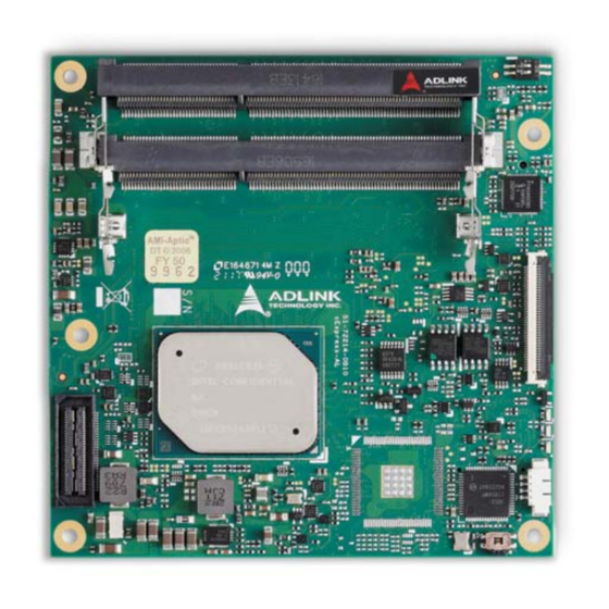
Summary of Contents for ADLINK Technology cExpress-AL
- Page 1 User’s Manual COM Express Compact Size Type 6 Module with Intel® Atom™, Pentium®, Celeron® SoC Manual Rev.: Revision Date: December 4, 2017 Part Number: 50-1J068-1000 Leading EDGE COMPUTING...
- Page 2 Preface Copyright Copyright 2017 ADLINK Technology, Inc. This document contains proprietary information protected by copyright. All rights are reserved. No part of this manual may be reproduced by any mechanical, electronic, or other means in any form without prior written permission of the manufacturer.
-
Page 3: Table Of Contents
Table of Contents Preface ..........................ii List of Figures ........................v List of Tables........................vi Introduction........................1 Specifications ......................3 2.1. Core System .......................3 2.2. Expansion Busses ......................3 2.3. Video........................... 4 2.4. Audio........................... 4 2.5. LAN..........................4 2.6. Multi I/O and Storage....................4 2.7. Serial I/O........................5 2.8. -
Page 4: Preface
4.7. Switch Settings ......................37 Smart Embedded Management Agent (SEMA) .............39 5.1. Board Specific SEMA Functions................40 System Resources ....................43 6.1. System Memory Map....................43 6.2. I/O Map ........................43 6.3. Interrupt Request (IRQ) Lines...................45 6.4. PCI Configuration Space Map ..................47 6.5. PCI Interrupt Routing Map ..................49 6.6. -
Page 5: List Of Figures
List of Figures Figure 1: cExpress-AL Functional Block Diagram..................7 Figure 2: cExpress-AL Mechanical Drawing ....................8 Figure 3: cExpress-AL Connector, Switch and LED Locations ............. 31 Figure 4: cExpress-AL and the DB40 Debug Module ................31 Figure 5: cExpress-AL Switch Locations....................37 Figure 6: COM Express Mounting Methods .................. - Page 6 List of Tables Table 1: cExpress-AL AB/CD Pin Definitions ...................9 Table 2: 40-pin Debug Connector Pin Definition ................... 32 Table 3: cExpress-AL LED Descriptions ....................33 Table 4: MIPI60 Debug Header Pin Definition ..................34 Table 5: Fan Connector Pin Definition ....................35 Table 6: BIOS Select and Mode Configuration Switch Settings............
-
Page 7: Introduction
The cExpress-AL has dual stacked SODIMM sockets for up to 8 GB non-ECC type DDR3L memory. Featured IO include a single Gigabit Ethernet port (IEEE 1588 support), USB 3.0 ports and USB 2.0 ports, SATA 6 Gb/s ports, and up to 5 PCIe x1 lanes. - Page 8 This page intentionally left blank. Introduction...
-
Page 9: Specifications
2. Specifications 2.1. Core System Dual or quad-core Intel® Atom™, Pentium® or Celeron® Processor SoC • Atom E3950 1.6/2.0GHz (Turbo), 400-650MHz (graphics), 12W (4C/1866) • Atom E3940 1.6/1.8GHz (Turbo), 400-600MHz (graphics), 9W (4C/1866) • Atom E3930 1.3/1.8GHz (Turbo), 400-550MHz (graphics), 6W (2C/1866) •... -
Page 10: Video
2.3. Video Intel® 9th generation LP graphics core architecture with up to 18 execution units Integrated on Processor supporting three independent displays • GPU Feature Support 3D graphics hardware acceleration • Support for DirectX12/11.3/10/9.3, OCL 2.0, OGL ES 3.0, OGL 4.3 •... -
Page 11: Serial I/O
Boot Device Support Windows 10 Linux Windows IOT Enterprise (Yocto) Core Storage only eMMC 5.0 OS Installation eMMC 5.0 Note: eMMC and SD functionality as an OS installation device may change dependent on Intel updates. Please contact your local sales representative for more information. -
Page 12: Power Specifications
2.11. Power Specifications AT and ATX mode (AT mode startup controlled by SEMA Board Controller) Power Modes ATX: 12V±5% / 5Vsb ±5% or AT = 12V±5% Standard Voltage Input ATX: 4.75-20 V / 5Vsb ±5% or AT = 4.75-20 V Wide Voltage Input ACPI 5.0 compliant, Smart Battery support Power Management... -
Page 13: Functional Diagram
8/16/32GB UART1 (build option) TPM 2.0 LPC to (build option) UART LPC bus SMBus SPI 0 BIOS GPIO SPI 1 BIOS 4x GPI, 4x GPO (SD) GP I2C SEMA DDC I2C LM73 SPI_CS# Figure 1: cExpress-AL Functional Block Diagram Specifications... -
Page 14: Mechanical Drawing
88.9 Side View All are dimensions shown in millimeters. Tolerances should be ± 0.25mm, unless otherwise noted. The tolerances of the module connector locating peg holes (16.50, 6.00] and [16.50, 18.00]) should be ±0.10mm. Figure 2: cExpress-AL Mechanical Drawing Specifications... -
Page 15: Pinouts And Signal Descriptions
3.1. AB/CD Pin Definitions The cExpress-AL is a Type 6 module supporting USB 3.0 upgrade signals and DDI channels on the CD connector All pins in the COM Express specification are described, including those not supported on the cExpress-AL. Those not supported on the cExpress-AL module are crossed out. - Page 16 Row A Row B Row C Row D Name Name Name Name USB6‐ USB7‐ DDI3_CTRLCLK_AUX+ DDI1_PAIR3+ USB6+ USB7+ DDI1_PAIR3‐ DDI3_CTRLDATA_AUX USB_6_7_OC# USB_4_5_OC# DDI3_DDC_AUX_SEL RSVD USB4‐ USB5‐ DDI3_PAIR0+ DDI2_PAIR0+ USB4+ USB5+ DDI3_PAIR0- DDI2_PAIR0‐ GND (fixed) GND (fixed) GND (fixed) GND (fixed) USB2‐...
- Page 17 Row A Row B Row C Row D Name Name Name Name GND (FIXED) GND (FIXED) GND (FIXED) GND (FIXED) LVDS_A_CK+ LVDS_B_CK+ PEG_RX9+ PEG_TX9+ LVDS_A_CK‐ LVDS_B_CK‐ PEG_RX9‐ PEG_TX9‐ LVDS_I2C_CK LVDS_BKLT_CTRL RSVD RSVD LVDS_I2C_DAT VCC_5V_SBY GPI3 VCC_5V_SBY PEG_RX10+ PEG_TX10+ RSVD VCC_5V_SBY PEG_RX10‐...
-
Page 18: Signal Description Terminology
3.2. Signal Description Terminology The following terms are used in the COM Express AB/CD Signal Descriptions below. Input to the Module Output from the Module Bi-directional input/output signal Open drain output I 3.3V Input 3.3V tolerant I 5V Input 5V tolerant O 3.3V Output 3.3V signal level O 5V... -
Page 19: Ab Signal Descriptions
3.3. AB Signal Descriptions 3.3.1. Audio Signals Signal Description PU/PD Comment HDA_RST# Reset output to CODEC, active low. O 3.3V HDA_SYNC Sample-synchronization signal to the O 3.3V CODEC(s). HDA_BITCLK Serial data clock generated by the I/O 3.3V external CODEC(s). - Page 20 3.3.3. LVDS/eDP LVDS Signal Description PU/PD Comment LVDS_A0+ LVDS Channel A differential pairs O LVDS LVDS is default. LVDS_A0- (through eDP to LVDS LVDS_A1+ bridge) LVDS_A1- LVDS_A2+ Note: eDP support LVDS_A2- available by build LVDS_A3+ option LVDS_A3- LVDS_A_CK+ LVDS Channel A differential clock O LVDS LVDS_A_CK- LVDS_B0+...
- Page 21 3.3.4. Gigabit Ethernet Gigabit Ethernet Description PU/PD Comment GBE0_MDI0+ Gigabit Ethernet Controller 0: Media Dependent Interface Twisted pair GBE0_MDI0- Differential Pairs 0, 1, 2, 3. The MDI can operate in 1000, Analog signals for GBE0_MDI1+ 100, and 10Mbit/sec modes. Some pairs are unused in...
- Page 22 3.3.6. PCI Express Signal Description PU/PD Comment PCIE_TX0+ PCI Express channel 0, Transmit AC coupled on module PCIE_TX0- Output differential pair. PCIE PCIE_RX0+ PCI Express channel 0, Receive Input I PCIE AC coupled off module PCIE_RX0- differential pair. PCIE_TX1+ PCI Express channel 1, Transmit AC coupled on module PCIE_TX1- Output differential pair.
- Page 23 3.3.8. Signal Description PU/PD Comment USB0+ USB differential data pairs for Port 0 I/O 3.3VSB USB 1.1/ 2.0 USB0- compliant USB1+ USB differential data pairs for Port 1 I/O 3.3VSB USB 1.1/ 2.0 USB1- compliant USB2+ USB differential data pairs for Port 1 I/O 3.3VSB...
- Page 24 3.3.9. USB Root Segmentation USB 3.0 Upgrade Port 3 xHCI Engine USB 2.0 USB 3.0 Upgrade Port 2 USB 2.0 USB 2.0 USB 2.0 USB 3.0 Upgrade Port 1 USB 2.0 USB 2.0 USB 3.0 Upgrade Port 0 USB 3.0 USB 3.0 USB 2.0 USB 2.0...
- Page 25 3.3.10. SPI (BIOS only) Signal Description PU/PD Comment SPI_CS# Chip select for Carrier Board SPI BIOS Flash. O 3.3VSB PU 10k Only supports CS0 3.3VSB SPI_MISO Data in to module from carrier board SPI BIOS I 3.3VSB flash. SPI_MOSI Data out from module to carrier board SPI BIOS O 3.3VSB...
- Page 26 Notes: GPO[0:3], PU 10k 3.3V is by build option for programming these pins to be GPI. GPI[0:3], PD 10k is by build option for programming these pins to be GPO. cExpress-AL supports an SD/GPIO muxed design, controlled by BIOS setting. See the table below for pin mapping.
- Page 27 SD/GPIO Pin Mapping GPIO Signal SD Signal Note GPI0 SD_DATA0 Bidirectional signal GPI1 SD_DATA1 Bidirectional signal GPI2 SD_DATA2 Bidirectional signal GPI3 SD_DATA3 Bidirectional signal GPO0 SD_CLK Output from COM Express, input to SD GPO1 SD_CMD Output from COM Express, input to SD...
- Page 28 Signal Description PU/PD Comment SUS_STAT# Indicates imminent suspend operation; used to notify O 3.3VSB LPC devices. Indicates system is in Suspend to RAM state. Active-low SUS_S3# O 3.3VSB output. An inverted copy of SUS_S3# on the carrier board (also known as “PS_ON”) may be used to enable the non-standby power on a typical ATX power supply.
-
Page 29: Cd Signal Descriptions
3.4. CD Signal Descriptions 3.4.1. USB 3.0 extension Signal Description PU/PD Comment USB_SSRX0- Additional Receive signal differential pairs for the I PCIE AC coupled off USB_SSRX0+ SuperSpeed USB data path on USB0 Module USB_SSTX0- Additional Transmit signal differential pairs for the... - Page 30 3.4.3. DDI Channels DDI 1 Signal Description PU/PD Comment DDI1_PAIR0+ Digital Display Interface1 O PCIE Pair 4 to Pair 6 are NOT differential pairs supported DDI1_PAIR0- DDI1_PAIR1+ DDI1_PAIR1- DDI1_PAIR2+ DDI1_PAIR2- DDI1_PAIR3+ DDI1_PAIR3- DDI1_PAIR4+ DDI1_PAIR4- DDI1_PAIR5+ DDI1_PAIR5- DDI1_PAIR6+ DDI1_PAIR6- DDI1_HPD Digital Display Interface Hot-Plug I PCIE Detect 100K...
- Page 31 DDI 2 Signal Description PU/PD Comment DDI2_PAIR0+ Digital Display Interface2 differential pairs DDI2_PAIR0- DDI2_PAIR1+ DDI2_PAIR1- DDI2_PAIR2+ DDI2_PAIR2- DDI2_PAIR3+ DDI2_PAIR3- DDI2_HPD 100K DDI2_CTRLCLK_AUX+ IF DDI2_DDC_AUX_SEL is floating I/O PCIe DP2_AUX+ 100K AC coupled on Module IF DDI2_DDC_AUX_SEL pulled high I/O OD HDMI2_CTRLCLK 3.3V...
- Page 32 Signal Description PU/PD Comment DDI3_DDC_AUX_SEL Selects the function of PD 1M DDI3_CTRLCLK_AUX+ and DDI3_CTRLDATA_AUX-. This pin shall have a 1M pull-down to logic ground on the Module. If this input is floating the AUX pair is used for the DP AUX+/- signals. If pulled-high the AUX pair contains the CRTLCLK and CTRLDATA signals.
- Page 33 Pin Name HDMI \ DVI DDI3_PAIR0+ DP3_LANE0+ TMDS3_DATA2+ DDI3_PAIR0- DP3_LANE0- TMDS3_DATA2- DDI3_PAIR1+ DP3_LANE1+ TMDS3_DATA1+ DDI3_PAIR1- DP3_LANE1- TMDS3_DATA1- DDI3_PAIR2+ DP3_LANE2+ TMDS3_DATA0+ DDI3_PAIR2- DP3_LANE2- TMDS3_DATA0- DDI3_PAIR3+ DP3_LANE3+ TMDS3_CLK+ DDI3_PAIR3- DP3_LANE3- TMDS3_CLK- DDI3_HPD DP3_HPD HDMI3_HPD DDI3_CTRLCLK_AUX+ DP3_AUX+ HDMI3_CTRLCLK DDI3_CTRLDATA_AUX- DP3_AUX- HDMI3_CTRLDATA DDI3_DDC_AUX_SEL 3.4.5.
- Page 34 Signal Description PU/PD Comment PEG_TX3- PEG_TX4+ PEG_TX4- PEG_TX5+ PEG_TX5- PEG_TX6+ PEG_TX6- PEG_TX7+ PEG_TX7- PEG_TX8+ PEG_TX8- PEG_TX9+ PEG_TX9- PEG_TX10+ PEG_TX10- PEG_TX11+ PEG_TX11- PEG_TX12+ PEG_TX12- PEG_TX13+ PEG_TX13- PEG_TX14+ PEG_TX14- PEG_TX15+ D101 PEG_TX15- D102 PEG_LANE_RV# D54 PCI Express Graphics lane reversal input I 1.05V Not supported strap.
- Page 35 Signal Pin # Description PU/PD Comment C1, C2, C5, C8, C11, Ground - DC power and signal and AC signal return C14, C21, C31, C41, path. C51, C60, C70, C73, All available GND connector pins shall be used and C76, C80, C84, C87, tied to carrier board GND plane.
- Page 36 This page intentionally left blank. Pinouts and Signal Descriptions...
-
Page 37: Module Interfaces
LED3 LED2 MIPI60 LED1 60-pin to CPU 4-pin BIOS Defaults RESET Switch Figure 3: cExpress-AL Connector, Switch and LED Locations cExpress-AL and the DB40 Debug Module For illustration purposes only Figure 4: cExpress-AL and the DB40 Debug Module Module Interfaces... -
Page 38: 40-Pin Debug Connector
4.2. 40-pin Debug Connector FPC Connector Type: FCI 59GF Flex 10042867 Pin Orientation 40-pin Debug Connector Pin Definition on the COM Express Module Pin Interface Signal Remark Interface Signal Remark VCC_SPI_IN SPI Power Input from flash TXD6 Program tool to module. HW need add Program interface MOS FET to switch SPI power... -
Page 39: Status Leds
Watchdog RESET WD LED = LED ON Rebooted after WD RESET WD LED = LED ON Rebooted after PWRBTN WD LED = LED OFF Rebooted after RESET BTN WD LED = LED OFF Table 3: cExpress-AL LED Descriptions Module Interfaces... -
Page 40: Mipi60 Debug Header
4.4. MIPI60 Debug Header Not all pins of the Intel MIPI60 connector are connected to the CombiProbe Intel x86/x64 MIPI60-C. ® Signal XDP Signal VREF_DEBUG TCK0 Open Drain Reset Out Reset In No Connect TRST_N PREQ_N PRDY_N VREF_TRACE PTI_0_CLK PTI_1_CLK No Connect PTI_1_DATA[0] PTI_0_DATA[0]... -
Page 41: Fan Connector
4.5. Fan Connector Connector Type: JVE 24W1125A-04M00 Pin Orientation 1 2 3 4 Pin Assignment Name Signal FAN_PWMOUT FAN_TACHIN Ground Table 5: Fan Connector Pin Definition Module Interfaces... -
Page 42: Bios Setup Defaults Reset Button
4.6. BIOS Setup Defaults Reset Button To perform a hardware reset of BIOS default settings, perform the following steps: 1. Shut down the system. 2. Press the BIOS Setup Defaults RESET Button continuously and boot up the system. You can release the button when the BIOS prompt screen appears 3. -
Page 43: Switch Settings
Switch Locations BIOS Select and Mode Configuration Switch Figure 5: cExpress-AL Switch Locations BIOS Select and Mode Configuration Switch The module has two BIOS chips and BIOS operation can be configured to "PICMG" or dual-BIOS "Failsafe" modes using the BIOS Select and Mode Configuration Switch, Pin 2. - Page 44 This page intentionally left blank. Module Interfaces...
-
Page 45: Smart Embedded Management Agent (Sema)
5. Smart Embedded Management Agent (SEMA) The onboard microcontroller (BMC) implements power sequencing and Smart Embedded Management Agent (SEMA) functionality. The microcontroller communicates via the System Management Bus with the CPU/chipset. The following functions are implemented: ‧ Total operating hours counter. Counts the number of hours the module has been run in minutes. -
Page 46: Board Specific Sema Functions
5.1.2. Main Current The BMC of the cExpress-AL implements a current monitor. The current can be read by calling the SEMA function “Get Main Current”. The function returns four 16-bit values divided in high-byte (MSB) and low-byte (LSB). These 4 values represent the last 4 currents drawn by the board. -
Page 47: Table 9: Sema Exception Codes
5.1.4. Exception Codes In case of an error, the BMC drives a blinking code on the blue Status LED (LED1). The same error code is also reported by the BMC Flags register. The Exception Code is not stored in the Flash Storage and is cleared when the power is removed. - Page 48 This page intentionally left blank. Smart Embedded Management Agent (SEMA)
-
Page 49: System Resources
6. System Resources 6.1. System Memory Map Address Range (hex) Description FF00_0000 – IFAW (BIOS) FFFF_FFFF FED0_0000 – HPET FEDF_33FF FEC0_0000 – IOAPIC FECF_FFFF 0K –1MB DOS DRAM 6.2. I/O Map I/O Address IOSF Primary IOSF SB Target Target 000h–01Fh... - Page 50 I/O Address IOSF Primary IOSF SB Target Target 063h P2SB ITSS (CPU I/F) 064h P2SB LPC/eSPI 065h P2SB ITSS (CPU I/F) 066h P2SB LPC/eSPI 067h P2SB ITSS (CPU I/F) 070h P2SB ITSS (CPU I/F), RTC, PMC 071h P2SB RTC, PMC 072h–073h P2SB RTC, PMC...
-
Page 51: Interrupt Request (Irq) Lines
I/O Address IOSF Primary IOSF SB Target Target 0B8h–0B9h P2SB ITSS (interrupt) 0BCh–0BDh P2SB ITSS (interrupt) 0C0h–0DFh P2SB Terminate 0F0h P2SB Terminate 170h–177h P2SB Terminate 2F8h–2FFh P2SB Serial Port 240h–24Fh P2SB Serial Port 2F8h–2FFh P2SB Serial Port 376h P2SB... - Page 52 APIC Mode IRQ# Typical Intterupt Resource Connected to Pin Available Counter 0 Keyboard controller IRQ1 via SERIRQ Cascade interrupt from slave PIC Serial Port 4 (COM3) IRQ3 via SERIRQ Note (1) Serial Port 3 (COM4) IRQ4 via SERIRQ Note (1) Note (1) Note (1) Note (1)
-
Page 53: Pci Configuration Space Map
6.4. PCI Configuration Space Map Logical Function Device Function Host Bridge DPTF (Camarillo) NPK (PSF ghost) Iunit Reserved (CSE) P2SB Shared SRAM Audio CSE-HECI1 CSE-HECI2 CSE-HECI3 CSE-fTPM (PSF ghost) CSE-HOFFL SATA PCIe-A 0 PCIe-A 1 PCIe-A 2 PCIe-A 3... - Page 54 Logical Function Device Function I2C 5 I2C 6 I2C 7 UART 0 UART 1 UART 2 UART 3 SPI 0 SPI 1 SPI 2 SD Card eMMC SDIO SMBUS System Resources...
-
Page 55: Pci Interrupt Routing Map
6.5. PCI Interrupt Routing Map PCIE PCIE PCIE PCIE PCIE PCIE Mobile PUNIT Line port1 port 2 port 3 port 4 Port 5 Port 6 IGFX Device Int0 INTA:22 INTB:23 INTC:22 INTD:23 INTA:20 INTB:21 NTD:19 Int1 INTB:23 INTC:20 INTD:23 INTA:20... -
Page 56: Smbus Address Table
6.6. SMBus Address Table Device Address DIMMA DIMMB Extend GPIO I210 USB2514BI LM73 PEX8605 B7h,C1h NXP(eDP to LVDS transmitter) C0h System Resources... -
Page 57: Bios Setup
7. BIOS Setup 7.1. Menu Structure This section presents the six primary menus of the BIOS Setup Utility. Use the following table as a quick reference for the contents of the BIOS Setup Utility. The subsections in this section describe the submenus and setting options for each menu item. -
Page 58: Main
7.2. Main 7.2.1. Main > BIOS Information Feature Options Description BIOS Vender Info only American Megatrends BIOS Version Info only ADLINK BIOS version Build Date Info only ADLINK BIOS Build Date MRC Version Info only Display MRC Version GOP Version Info only Display GOP Version TXE FW Version... - Page 59 Feature Options Description Info only Boot Cycles The Boot counter is increased after a HW- or SW- Reset or after a successful power-up. Info only The boot reason is the event which causes the reboot Boot Reason of the system.
-
Page 60: Advanced
7.3. Advanced This menu contains the settings for most of the user interfaces in the system. 7.3.1. Advanced > CPU Configuration Feature Options Description CPU Configuration Info only Socket 0 CPU Information Submenu Socket Specific CPU Information. Stocket 0 CPU information Info only CPU Signature Info only... - Page 61 Feature Options Description Core C9 Core C8 Core C7 Core C6 Core C1 Unlimited C-State Auto Demotion Disabled Configure C-State Auto Demotion C-State Un-demotion Disabled Configure C-State Auto Un-demotion Power Limit 1 Enable Disabled Enable / Disable Power Limit 1...
- Page 62 Feature Options Description Active Processor Cores Number of cores to enable in each processor Disabled Enabled package. Intel Virtualization Technology Disabled When enabled, a VMM can utilize the additional hardware capabilities provided by Vanderpool Enabled Technology. VT-d Disabled Enable / Disable CPU VT-d Enabled Bi-directional PROCHOT Disabled...
- Page 63 7.3.3. Advanced > Power Management Feature Options Description Power Management Info only Enable ACPI Auto Configuration Enables or Disables BIOS ACPI Auto Configuration. Disabled Enabled Enable Hibernation Disabled Enable or Disable System ability to Hibernate (OS/S4 Sleep State). Enabled This option maybe not effective with some OS.
- Page 64 Feature Options Description SEMA Firmware Info Only Display SEMA Firmware Version. Build Date Info Only Display SEMA Firmware Build Date. SEMA Bootloader Info Only Display SEMA Bootloader Version. Build Date Info Only Display SEMA Bootloader Build Date. SEMA Features Submenu Display SEMA Supported Features SEMA Supported Features Info only...
- Page 65 7.3.5.2. Advanced > Thermal Management > Smart Fan Feature Options Description Smart Fan Info Only CPU Smart Fan Temperature CPU Sensor CPU Smart Fan Temperature Source Source Board Sensor CPU Fan Mode AUTO (Smart Fan) CPU Fan Mode Fan Off...
- Page 66 Feature Options Description Device Settings Info Only Display IO / IRQ information of COM Port. Change Settings Select an optimal setting for Super IO Device. Auto IO=240h; IRQ=10; IO=240h; IRQ=3,4,5,6,7,10,11,12 IO=248h; IRQ=3,4,5,6,7,10,11,12 IO=250h; IRQ=3,4,5,6,7,10,11,12 IO=258h; IRQ=3,4,5,6,7,10,11,12 7.3.8.2. Advanced > Super IO Configuration > Serial Port 2 Configuration (NCT5104D) Feature Options Description...
- Page 67 7.3.8.4. Advanced > Super IO Configuration > Serial Port 2 Configuration (W83627DHG) Feature Options Description Serial Port 2 Configuration Submenu Set Parameters of Serial Port 2 (COMB). Serial Port 2 Configuration Info only Serial Port Disableed Enable or Disable Serial Port (COM).
- Page 68 Feature Options Description COM4 Info only Console Redirection Enabled Console Redirection Enable or Disable. Disabled Console Redirection Settings Submenu The settings specify how the host computer and the remote computer (which the user is using) will exchange data. Both computers should have the same or compatible settings.
- Page 69 Feature Options Description Recorder Mode With this mode enabled only text will be sent. Disabled Enabled This is to capture Terminal data. Resolution 100x31 Enabled On Legacy OS, the Number of Rows and Columns supported redirection Disabled Legacy OS Redirection Resolution...
- Page 70 Feature Options Description VT-UTF8 Combo Key Support Enable VT-UTF8 Combination Key Support for Enabled Disabled ANSI/VT100 terminals Recorder Mode With this mode enabled only text will be sent. Disabled Enabled This is to capture Terminal data. Resolution 100x31 Enabled On Legacy OS, the Number of Rows and Columns supported redirection Disabled Legacy OS Redirection Resolution...
- Page 71 Feature Options Description flow. Once the buffers are empty, a 'start' signal can be sent to re-start the flow. Hardware flow control uses two wires to send start/stop signals. VT-UTF8 Combo Key Support Enable VT-UTF8 Combination Key Support for...
- Page 72 Feature Options Description Flow control can prevent data loss from buffer Flow Control None overflow. When sending data, if the receiving buffers Hardware RTS/CTS are full, a 'stop' signal can be sent to stop the data flow. Once the buffers are empty, a 'start' signal can be sent to re-start the flow.
- Page 73 Feature Options Description USB hardware delays and time-outs: Info Only USB transfer rime-out 1 sec The time-out value for Control, Bulk, and Interrupt 5sec transfers. 10sec 20 sec Device reset time-out 10 sec USB mass storage device Start Unit command time- out.
- Page 74 Feature Options Description Platform hierarchy Disable Enable or Disable Platform Hierarchy Enable Disable Storage Hierarchy Enable or Disable Storage Hierarchy Enable Endorsement Hierarchy Disable Enable or Disable Endorsement Hierarchy Enable TPM2.0 UEFI Spec Version TCG_1_2 Select the TCG2 Spec Version Support, TCG_1_2: the Compatible mode for Win8/Win10, TCG_2 TCG_2: Support new TCG2 protocol and event format...
-
Page 75: Chipset
7.4. Chipset 7.4.1. Chipset > North Bridge Feature Options Description Memory Information Info only Total Memory Info only Display Total Memory Size. Display Memory Vlotage. Memory Vlotage Info only Display Installed Memory Slot0 Information. Memory Slot0 Info only Display Installed Memory Slot1 Information. - Page 76 Feature Options Description Select LFP panel used by Internal Graphics Device by LFP Panel Type Auto selecting the appropriate setup item. 640x480 800x600 1024x768 1280x1024 1400x1050 1600x1200 1366x768 1680x1050 1920x1200 1440x900 1600x900 1280x800 1920x1080 2048x1536 Set GOP Brightness Level. GOP Brightness Level IGD Configuration Info only Enable: Enable Integrated Graphics Device (IGD)
- Page 77 7.4.4. Chipset > South Cluster Configuration Feature Options Description HD-Audio Configuration Submenu HD-Audio Configuration Setting. PCI Express Configuration Setting. PCI Express Configuration Submenu Press <Enter> to select the SATA Device SATA Drives Submenu Configuration Setup option. SSC Configuration Settings.
- Page 78 Chipset > South Cluster Configuration > PCI Express Configuration > PCI Express Root Port 1 Feature Options Description Control the PCI Express Root Port. PCI Express Root Port 1 Disable AUTO: To disable unused root port automatically for Enable the most optimum power savings. Auto Enable: Enable PCIe root port.
- Page 79 Feature Options Description PCH PCIE Latency Reporting Enable/Disable PCH PCIE LTR Disable Enable Snoop Latency Override for PCH PCIE. Disabled Snoop Latency Override Disabled: Disable override. Manual Manual: Manually enter override values. Auto Auto (default): Maintain default BIOS flow.
- Page 80 Feature Options Description PCI Express PME SCI Enable/Disable PME SCI Disable Enable PCI Express Hot Plug Enable/Disable Hot Plug Disable Enable Configure PCIe Speed PCIe Speed Auto Gen1 Gen2 Transmitter Half Swing Enable/Disable. Transmitter Half Swing Disable Enable Extra Bus Reserved (0-7) for bridges behind this Root Extra Bus Reserved Bridge Reserved Memory and Prefetchable Memory (1-...
- Page 81 Feature Options Description PCI Express Device Non-Fatal Error Reporting NFER Disable Enable/Disable Enable PCI Express Device Correctable Error Reporting Disable Enable/Disable Enable PCI Express Completion Timer TO Enable/Disable. Default Setting 16-15 ms 65-210 ms 260-900 ms 1-3.5 s Disable...
- Page 82 Chipset > South Cluster Configuration > PCI Express Configuration > PCI Express Root Port 4 Feature Options Description Control the PCI Express Root Port. PCI Express Root Port 4 Disable AUTO: To disable unused root port automatically for Enable the most optimum power savings. Auto Enable: Enable PCIe root port.
- Page 83 Feature Options Description PCH PCIE Latency Reporting Enable/Disable PCH PCIE LTR Disable Enable Snoop Latency Override for PCH PCIE. Disabled Snoop Latency Override Disabled: Disable override. Manual Manual: Manually enter override values. Auto Auto (default): Maintain default BIOS flow.
- Page 84 Feature Options Description Enable/Disable SATA Port 0 DevSlp. Board rework for SATA Port 0 DevSlp Disabled LP needed before enable. Enabled Enable/Disable DITO Configuration DITO Configuration Disabled Enabled DITO Value. DITO Value Note. DITO Value can be accessed if DITO Configuration item must enable.
- Page 85 Feature Options Description Select SD Card or GPIO function. SD Card/GPIO Mode GPIO SD Card 7.4.4.5. Chipset > South Cluster Configuration > USB Configuration Feature Options Description Enable / Disable XHCI Pre-Boot Driver support. XHCI Pre-Boot Driver Disabled Enabled...
-
Page 86: Security Menu
7.5. Security Menu 7.5.1. Security > Password Description Feature Options Description Password Description Info only Setup Administrator Password Enter Password Set Setup Administrator Password User Password Enter Password Set User Password Secure Boot Submenu Customizable Secure Boot settings. System Mode Info only Secure Boot Info only... -
Page 87: Save & Exit Menu
Feature Options Description Boot Option #6 USB Floppy Set the system boot order. Boot Option #7 USB Lan Set the system boot order. Boot Option #8 Network Set the system boot order. 7.7. Save & Exit Menu 7.7.1. Save and Exit... - Page 88 This page intentionally left blank. BIOS Setup...
-
Page 89: Bios Checkpoints, Beep Codes
8. BIOS Checkpoints, Beep Codes This section of this document lists checkpoints and beep codes generated by AMI Aptio BIOS. The checkpoints defined in this document are inherent to the AMIBIOS generic core, and do not include any chipset or board specific checkpoint definitions. -
Page 90: Status Code Ranges
8.1. Status Code Ranges Status Code Description Range 0x01 – 0x0B SEC execution 0x0C – 0x0F SEC errors 0x10 – 0x2F PEI execution up to and including memory detection 0x30 – 0x4F PEI execution after memory detection 0x50 – 0x5F PEI errors 0x60 –... - Page 91 SEC Error Codes 0x0C – 0x0D Reserved for future AMI SEC error codes 0x0E Microcode not found 0x0F Microcode not loaded 8.2.2. SEC Beep Codes None 8.2.3. PEI Phase Status Code Description Progress Codes 0x10 PEI Core is started...
- Page 92 Status Code Description 0x35 CPU post-memory initialization. Boot Strap Processor (BSP) selection 0x36 CPU post-memory initialization. System Management Mode (SMM) initialization 0x37 Post-Memory North Bridge initialization is started 0x38 Post-Memory North Bridge initialization (North Bridge module specific) 0x39 Post-Memory North Bridge initialization (North Bridge module specific) 0x3A Post-Memory North Bridge initialization (North Bridge module specific) 0x3B...
- Page 93 Status Code Description S3 Resume Error Codes 0xE8 S3 Resume Failed 0xE9 S3 Resume PPI not Found 0xEA S3 Resume Boot Script Error 0xEB S3 OS Wake Error 0xEC-0xEF Reserved for future AMI error codes Recovery Progress Codes 0xF0...
- Page 94 8.2.5. DXE Status Codes Status Code Description 0x60 DXE Core is started 0x61 NVRAM initialization 0x62 Installation of the South Bridge Runtime Services 0x63 CPU DXE initialization is started 0x64 CPU DXE initialization (CPU module specific) 0x65 CPU DXE initialization (CPU module specific) 0x66 CPU DXE initialization (CPU module specific) 0x67...
- Page 95 Status Code Description 0x95 PCI Bus Request Resources 0x96 PCI Bus Assign Resources 0x97 Console Output devices connect 0x98 Console input devices connect 0x99 Super IO Initialization 0x9A USB initialization is started 0x9B USB Reset 0x9C USB Detect 0x9D USB Enable 0x9E –...
- Page 96 Status Code Description 0xB8 – 0xBF Reserved for future AMI codes 0xC0 – 0xCF OEM BDS initialization codes DXE Error Codes 0xD0 CPU initialization error 0xD1 North Bridge initialization error 0xD2 South Bridge initialization error 0xD3 Some of the Architectural Protocols are not available 0xD4 PCI resource allocation error.
-
Page 97: Oem-Reserved Checkpoint Ranges
Status Code Description 0x10 System is waking up from the S1 sleep state 0x20 System is waking up from the S2 sleep state 0x30 System is waking up from the S3 sleep state 0x40 System is waking up from the S4 sleep state 0xAC System has transitioned into ACPI mode. - Page 98 This page intentionally left blank. BIOS Checkpoints, Beep Codes...
-
Page 99: Mechanical Information
9. Mechanical Information 9.1. Board-to-Board Connectors To allow for different stacking heights, the receptacles for COM Express carrier boards are available in two heights: 5 mm and 8 mm. When 5 mm receptacles are chosen, the carrier board should be free of components. -
Page 100: Thermal Solution
9.2. Thermal Solution 9.2.1. Heat Spreaders The function of the heat spreader is to ensure an identical mechanical profile for all COM Express modules. By using a heat spreader, the thermal solution that is built on top of the module is compatible with all COM Express modules. - Page 101 Step 3: Assemble the heatsink onto the COM Express module. Use the four M2.5, L=6mm screws provided to fasten the heatsink to the module. Step 4: Place the COM Express module and heatsink assembly onto the connectors on the carrier board as shown.
- Page 102 Step 6: If you are installing a heatsink with a fan, plug the fan connector into the carrier board as shown. Mechanical Information...
-
Page 103: Mounting Methods
9.3. Mounting Methods There are several standard ways to mount the COM Express module with a thermal solution onto a carrier board. In addition to the choice of 5 mm or 8mm board-to-board connectors, there is the choice of Top and Bottom mounting. -
Page 104: Standoff Types
9.4. Standoff Types The standoffs available for Top and Bottom mounting methods are shown below. Note that threaded standoffs are DIP type and through-hole standoffs are SMT type. Other types not listed are available upon request. 5mm through-hole standoff (SMT type) 5mm threaded standoff (DIP type) P/N: 33-72000-0050 P/N: 33-72016-0050... -
Page 105: Safety Instructions
Safety Instructions Read and follow all instructions marked on the product and in the documentation before you operate your system. Retain all safety and operating instructions for future use. • Please read these safety instructions carefully. • Please keep this User‘s Manual for later reference. -
Page 106: Getting Service
5215 Hellyer Avenue, #110, San Jose, CA 95138, USA Tel: +1-408-360-0200 Toll Free: +1-800-966-5200 (USA only) Fax: +1-408-360-0222 Email: info@adlinktech.com ADLINK Technology (China) Co., Ltd. Address: 300 Fang Chun Rd., Zhangjiang Hi-Tech Park, Pudong New Area Shanghai, 201203 China Tel: +86-21-5132-8988 Fax: +86-21-5132-3588 Email: market@adlinktech.com...
Need help?
Do you have a question about the cExpress-AL and is the answer not in the manual?
Questions and answers