Xilinx VC707 User Manual
Evaluation board for the virtex-7 fpga
Hide thumbs
Also See for VC707:
- User manual (116 pages) ,
- Manual (82 pages) ,
- Getting started (24 pages)

Related Manuals for Xilinx VC707


Summary of Contents for Xilinx VC707
- Page 1 VC707 Evaluation Board for the Virtex-7 FPGA User Guide UG885 (v1.2) February 1, 2013...
-
Page 2: Revision History
Limited Warranties which can be viewed at http://www.xilinx.com/warranty.htm; IP cores may be subject to warranty and support terms contained in a license issued to you by Xilinx. Xilinx products are not designed or intended to be fail-safe or for use in any application requiring fail-safe performance;... -
Page 3: Table Of Contents
VC707 Board Features ........ - Page 4 Appendix D: Board Setup Installing VC707 Board in a PC Chassis ........93...
-
Page 5: Chapter 1: Vc707 Evaluation Board Features
Chapter 1 VC707 Evaluation Board Features Overview The VC707 evaluation board for the Virtex®-7 FPGA provides a hardware environment for developing and evaluating designs targeting the Virtex-7 XC7VX485T-2FFG1761C FPGA. The VC707 board provides features common to many embedded processing systems, including a DDR3 SODIMM memory, an 8-lane PCI Express®... - Page 6 Chapter 1: VC707 Evaluation Board Features • Ethernet PHY SGMII interface (RJ-45 connector) • PCI Express endpoint connectivity • Gen1 8-lane (x8) • Gen2 8-lane (x8) • SFP+ Connector • 10/100/1000 tri-speed Ethernet PHY • USB-to-UART bridge • HDMI codec •...
-
Page 7: Feature Descriptions
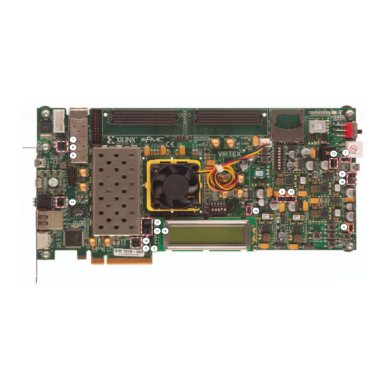
Figure 1-1. The VC707 board schematics are available for download from: www.xilinx.com/products/boards-and-kits/EK-V7-VC707-G.htm The VC707 board can be damaged by electrostatic discharge (ESD). Follow standard ESD prevention measures when handling the board X-Ref Target - Figure 1-1 1 GB DDR3 Memory... - Page 8 Chapter 1: VC707 Evaluation Board Features X-Ref Target - Figure 1-2 Round callout references a component Square callout references a component on the front side of the board on the back side of the board User rotary switch located under LCD...
-
Page 9: Virtex-7 Xc7Vx485T-2Ffg1761C Fpga
The VC707 board supports two of the five 7 series FPGA configuration modes: • Master BPI using the onboard Linear BPI Flash memory • JTAG using a type-A to micro-B USB cable for connecting the host PC to the VC707 board configuration port VC707 Evaluation Board www.xilinx.com... - Page 10 There are 17 I/O banks available on the Virtex-7 device. Sixteen I/O banks are available on the VC707 board, bank 31 is not used. The voltages applied to the FPGA I/O banks used by the VC707 board are listed in Table 1-3.
-
Page 11: Ddr3 Memory
The connections between the DDR3 memory and the FPGA are listed in Table 1-4. Table 1-4: DDR3 Memory Connections to the FPGA J1 DDR3 Memory FPGA (U1) Net Name Pin Number Pin Name DDR3_A0 DDR3_A1 DDR3_A2 DDR3_A3 DDR3_A4 DDR3_A5 DDR3_A6 DDR3_A7 DDR3_A8 VC707 Evaluation Board www.xilinx.com UG885 (v1.2) February 1, 2013... - Page 12 Chapter 1: VC707 Evaluation Board Features Table 1-4: DDR3 Memory Connections to the FPGA (Cont’d) J1 DDR3 Memory FPGA (U1) Net Name Pin Number Pin Name DDR3_A9 DDR3_A10 A10/AP DDR3_A11 DDR3_A12 A12_BC_N DDR3_A13 DDR3_A14 DDR3_A15 DDR3_BA0 DDR3_BA1 DDR3_BA2 DDR3_D0 DDR3_D1...
- Page 13 DQ38 DDR3_D39 DQ39 DDR3_D40 DQ40 DDR3_D41 DQ41 DDR3_D42 DQ42 DDR3_D43 DQ43 DDR3_D44 DQ44 DDR3_D45 DQ45 DDR3_D46 DQ46 DDR3_D47 DQ47 DDR3_D48 DQ48 DDR3_D49 DQ49 DDR3_D50 DQ50 DDR3_D51 DQ51 DDR3_D52 DQ52 DDR3_D53 DQ53 VC707 Evaluation Board www.xilinx.com UG885 (v1.2) February 1, 2013...
- Page 14 Chapter 1: VC707 Evaluation Board Features Table 1-4: DDR3 Memory Connections to the FPGA (Cont’d) J1 DDR3 Memory FPGA (U1) Net Name Pin Number Pin Name DDR3_D54 DQ54 DDR3_D55 DQ55 DDR3_D56 DQ56 DDR3_D57 DQ57 DDR3_D58 DQ58 DDR3_D59 DQ59 DDR3_D60 DQ60...
-
Page 15: Linear Bpi Flash Memory
DDR3_CLK1_P CK1_P The VC707 DDR3 SODIMM interface adheres to the constraints guidelines in the DDR3 Design Guidelines section of UG586, 7 Series FPGAs Memory Interface Solutions User Guide. The VC707 DDR3 SODIMM interface is a 40Ω impedance implementation. Other memory interface details are available in UG586 and UG473, 7 Series FPGAs Memory Resources User Guide. - Page 16 Chapter 1: VC707 Evaluation Board Features 80 MHz oscillator connected to the FPGA's EMCCLK pin with a bitstream that has been built to divide the configuration clock by two. The division is necessary to remain within the synchronous read timing specifications of the flash memory.
- Page 17 The configuration section of UG470, 7 Series FPGAs Configuration User Guide provides details on the Master BPI configuration mode. Figure 1-4 shows the connections of the linear BPI Flash memory on the VC707 board. For more details, see the Numonyx PC28F00AG18FE data sheet [Ref VC707 Evaluation Board www.xilinx.com...
-
Page 18: Usb 2.0 Ulpi Transceiver
[Figure 1-2, callout 4] The VC707 board uses a Standard Microsystems Corporation USB3320 USB 2.0 ULPI Transceiver (U8) to support a USB connection to the host computer. A USB cable is supplied in the VC707 Evaluation Kit (type-A connector to host computer, mini-B connector to VC707 board connector J2). - Page 19 1-7. Table 1-7: USB 2.0 ULPI Transceiver Connections to the FPGA FPGA (U1) Pin Net Name USB3320 (U8) Pin AV36 USB_SMSC_DATA0 AW36 USB_SMSC_DATA1 BA34 USB_SMSC_DATA2 BB34 USB_SMSC_DATA3 BA36 USB_SMSC_DATA4 AT34 USB_SMSC_DATA5 VC707 Evaluation Board www.xilinx.com UG885 (v1.2) February 1, 2013...
-
Page 20: Sd Card Interface
[Figure 1-2, callout 5] The VC707 board includes a secure digital input/output (SDIO) interface to provide user-logic access to general purpose nonvolatile SDIO memory cards and peripherals. The SD card slot is designed to support 50 MHz high speed SD cards. - Page 21 Schematic Net Name Pin Number Pin Name Pin Number Pin Name AR32 SDIO_SDWP SDWP AP32 SDIO_SDDET SDDET AP30 SDIO_CMD_LS AN30 SDIO_CLK_LS AV31 SDIO_DAT2_LS DAT2 AU31 SDIO_DAT1_LS DAT1 AR30 SDIO_DAT0_LS DAT0 AT30 SDIO_CD_DAT3_LS CD_DAT3 VC707 Evaluation Board www.xilinx.com UG885 (v1.2) February 1, 2013...
-
Page 22: Usb Jtag
UG885_c1_07_021412 Figure 1-7: JTAG Chain Block Diagram When an FMC mezzanine card is attached to the VC707 board it is automatically added to the JTAG chain through electronically controlled single-pole single-throw (SPST) switches U27 and U28. The SPST switches are in a normally closed state and transition to an open state when an FMC mezzanine card is attached. - Page 23 Translator FMC2_PRSNT_M2C_B_LS AG32 FMC1_PRSNT_M2C_B_LS AM31 VCC3V3 VCC1V8 VCC3V3 VCC1V8 SN74AVC1T45 Voltage Bank 0 SN74AVC2T45 Translator FPGA_TDI_BUF Voltage Translator FPGA_TMS_BUF FPGA_TCK_BUF VCC3V3 VCC1V8 JTAG_TDO SN74AVC1T45 Voltage Translator UG855_c1_08_021412 Figure 1-8: JTAG Circuit VC707 Evaluation Board www.xilinx.com UG885 (v1.2) February 1, 2013...
-
Page 24: Clock Generation
Chapter 1: VC707 Evaluation Board Features Clock Generation The VC707 board provides five clock sources for the FPGA. Table 1-9 lists the source devices for each clock. Table 1-9: VC707 Board Clock Sources Clock Clock Name Description Source System Clock SiT9102 2.5V LVDS 200 MHz Fixed Frequency Oscillator (SiTime). - Page 25 [Figure 1-2, callout 7] The VC707 board has a LVDS 200 MHz oscillator (U51) soldered onto the back side of the board and wired to an FPGA MRCC clock input on bank 38. This 200 MHz signal pair is named SYSCLK_P and SYSCLK_N, which are connected to FPGA U1 pins E19 and E18 respectively.
- Page 26 Chapter 1: VC707 Evaluation Board Features X-Ref Target - Figure 1-10 VCC3V3 VCC3V3 C192 0.01 μF 25V 4.7KΩ 5% Si570 Programmable Oscillator USER CLOCK SDA To I 2 C USER CLOCK N CLK- 10 MHz - 810 MHz Bus Switch...
- Page 27 [Figure 1-2, callout The VC707 board includes a pair of SMA connectors for a GTX clock wired to GTX Quad bank 113. This differential clock has signal names SMA_MGT_REFCLK_P and SMA_REFCLK_N, which are connected to FPGA U1 pins AK8 and AK7 respectively.
-
Page 28: Gtx Transceivers
The GTX transceivers in 7 series FPGAs are grouped into four channels described as Quads. The reference clock for a Quad can be sourced from the Quad above or Quad below the GTX Quad of interest. There are four GTX Quads on the VC707 board with connectivity as shown here: www.xilinx.com... - Page 29 GTX Interface Connections for FPGA U1 Transceiver Bank Net Name Connections MGT_BANK_113 GTXE2_CHANNEL_X1Y0 GTXE2_CHANNEL_X1Y1 SGMII GTXE2_CHANNEL_X1Y2 SFP+ GTXE2_CHANNEL_X1Y3 MGTREFCLK0 SGMII_CLK MGTREFCLK1 SMA_MGT_REFCLK MGT_BANK_114 GTXE2_CHANNEL_X1Y4 PCIe7 GTXE2_CHANNEL_X1Y5 PCIe6 GTXE2_CHANNEL_X1Y6 PCIe5 GTXE2_CHANNEL_X1Y7 PCIe4 MGTREFCLK0 Si5324 MGTREFCLK1 VC707 Evaluation Board www.xilinx.com UG885 (v1.2) February 1, 2013...
- Page 30 Chapter 1: VC707 Evaluation Board Features Table 1-11: GTX Interface Connections for FPGA U1 (Cont’d) Transceiver Bank Net Name Connections MGT_BANK_115 GTXE2_CHANNEL_X1Y8 PCIe3 GTXE2_CHANNEL_X1Y9 PCIe2 GTXE2_CHANNEL_X1Y10 PCIe1 GTXE2_CHANNEL_X1Y11 PCIe0 MGTREFCLK0 MGTREFCLK1 PCIe_CLK MGT_BANK_116 GTXE2_CHANNEL_X1Y12 FMC2 HPC DP4 GTXE2_CHANNEL_X1Y13 FMC2 HPC DP5...
-
Page 31: Pci Express Endpoint Connectivity
85Ω ±10%. The PCIe clock is routed as a 100Ω differential pair. The 7 series FPGAs GTX transceivers are used for multi-gigabit per second serial interfaces. The XC7VX485T-2FFG1761C FPGA (-2 speed grade) included with the VC707 board supports up to Gen2 x8. - Page 32 Chapter 1: VC707 Evaluation Board Features Table 1-12: PCIe Edge Connector Connections (Cont’d) PCIe Edge Connector (P1) FPGA (U1) FHG1761 Net Name Function Placement Name PCIE_RX3_N PETn3 Integrated Endpoint block receive pair GTXE2_CHANNEL_X0Y16 PCIE_RX4_P PETp4 Integrated Endpoint block receive pair...
- Page 33 Placement Pin Name MGTXTXP0_114_AK4 PCIE_TX7_P PERp7 GTXE2_CHANNEL_X0Y12 MGTXTXN0_114_AK3 PCIE_TX7_N PERn7 GTXE2_CHANNEL_X0Y12 MGTXRXP0_114_AG6 PCIE_RX7_P PETp7 GTXE2_CHANNEL_X0Y12 MGTXRXN0_114_AG5 PCIE_RX7_N PETn7 GTXE2_CHANNEL_X0Y12 PCIE_TX6_P PERp6 GTXE2_CHANNEL_X0Y13 MGTXTXP1_114_AJ2 PCIE_TX6_N PERn6 GTXE2_CHANNEL_X0Y13 MGTXTXN1_114_AJ1 PCIE_RX6_P PETp6 GTXE2_CHANNEL_X0Y13 MGTXRXP1_114_AF4 VC707 Evaluation Board www.xilinx.com UG885 (v1.2) February 1, 2013...
- Page 34 7 Series FPGAs Integrated Block for PCI Express User Guide (AXI). SFP/SFP+ Module Connector [Figure 1-2, callout 14] The VC707 board contains a small form-factor pluggable (SFP+) connector and cage assembly P3 that accepts SFP or SFP+ modules. Figure 1-16 shows the SFP+ module connector circuitry.
-
Page 35: Sfp/Sfp+ Module Connector
SFP_RS1 VCC3V3 VCC3V3 R392 R391 HDR_1X3 4.7KΩ 4.7KΩ SFP_RS0 1-2: FULL BW RX 1-2: FULL BW TX 2-3: LOW BW RX 2-3: LOW BW TX UG885_c1_16_011813 Figure 1-16: SFP+ Module Connector VC707 Evaluation Board www.xilinx.com UG885 (v1.2) February 1, 2013... -
Page 36: 10/100/1000 Tri-Speed Ethernet Phy
[Figure 1-2, callout 15] The VC707 board utilizes the Marvell Alaska PHY device (88E1111) U50 for Ethernet communications at 10, 100, or 1000 Mb/s. The board supports SGMII mode only. The PHY connection to a user-provided Ethernet cable is through a Halo HFJ11-1G01E RJ-45 connector (P4) with built-in magnetics. -
Page 37: Sgmii Gtx Transceiver Clock Generation
GTX transceiver (clock pins AH8 (P) and AH7 (N)) driving the SGMII interface. Series AC coupling capacitors are present to allow the clock input of the FPGA to set the common mode voltage. Figure 1-17 shows the Ethernet SGMII clock source. VC707 Evaluation Board www.xilinx.com UG885 (v1.2) February 1, 2013... -
Page 38: Usb-To-Uart Bridge
USB port. The USB cable is supplied in the VC707 Evaluation Kit (Type-A end to host computer, Type mini-B end to VC707 board connector J17). The CP2103GM is powered by the USB 5V provided by the host PC when the USB cable is plugged into the USB port on the VC707 board. -
Page 39: Hdmi Video Output
HDMI Video Output [Figure 1-2, callout 18] The VC707 board provides a High-Definition Multimedia Interface (HDMI™) video output using the Analog Devices ADV7511KSTZ-P HDMI transmitter (U48). The HDMI output is provided on a Molex 500254-1927 HDMI type-A connector (P2). The ADV7511 is wired to support 1080P 60 Hz YCbCr and RGB video modes through 36-bit input data mapping. - Page 40 Chapter 1: VC707 Evaluation Board Features Figure 1-18 shows the HDMI codec circuit. X-Ref Target - Figure 1-18 VCC3V3 VADJ VCC2V5 R104 R106 2.43K 2.43K SIT8102 R105 1/10W 1/10W 12.00000 MHZ 2.43K 50PPM 1/10W ADV7511 HDMI_INT IIC_SCL_HDMI CEC_CLK IIC_SDA_HDMI HDMI_SPDIF_OUT...
- Page 41 HDMI_D15 AM23 HDMI_D16 AN24 HDMI_D17 AY24 HDMI_D18 BB22 HDMI_D19 BA22 HDMI_D20 BA25 HDMI_D21 AY25 HDMI_D22 AY22 HDMI_D23 AY23 HDMI_D24 AV24 HDMI_D25 AU24 HDMI_D26 AW21 HDMI_D27 AV21 HDMI_D28 AT24 HDMI_D29 AR24 HDMI_D30 VC707 Evaluation Board www.xilinx.com UG885 (v1.2) February 1, 2013...
- Page 42 Chapter 1: VC707 Evaluation Board Features Table 1-21: FPGA to HDMI Codec Connections (ADV7511) (Cont’d) ADV7511 (U48) FPGA (U1) Pin Schematic Net Name Pin Number Pin Name AU21 HDMI_D31 AT21 HDMI_D32 AW22 HDMI_D33 AW23 HDMI_D34 AV23 HDMI_D35 AP21 HDMI_DE AR23...
-
Page 43: Lcd Character Display (16 X 2)
UG885_c1_20_020612 Figure 1-20: LCD Interface Circuit The VC707 board base board uses a male Samtec MTLW-107-07-G-D-265 2x7 header (J23) with 0.025-inch square posts on 0.100-inch centers for connecting to a Samtec SLW-107-01-L-D female socket on the LCD display panel assembly. The LCD header... -
Page 44: I 2 C Bus
8]. Choose the S162D model full spec download arrow. C Bus [Figure 1-2, callout 20] The VC707 board implements a single I C port on the FPGA (IIC_SDA_MAIN, IIC_SDA_SCL), which is routed through a 1-to-8 channel I C bus switch (U52). The bus switch can operate at speeds up to 400 kHz. - Page 45 Feature Descriptions The VC707 board I C bus topology is shown in Figure 1-22. X-Ref Target - Figure 1-22 PCA9548 1 2 C 1-to-8 Bus Switch CH0 - USER_CLK_SDL/SCL CH1 - FMC1_HPC_IIC_SDA/SCL FPGA Bank 15 CH2 - FMC2_HPC_IIC_SDA/SCL (2.5V) CH3 - EEPROM_IIC_SDA/SCL...
-
Page 46: Status Leds
TPS51200 Power Good (U23) User I/O [Figure 1-2, callout - 26] The VC707 board provides the following user and general purpose I/O capabilities: • Eight user LEDs (callout 22) • GPIO_LED_[7-0]: DS9, DS8, DS7, DS6, DS5, DS4, DS3, DS2 •... - Page 47 UG855_c1_23_020612 Figure 1-23: User LEDs CPU Reset Pushbutton Figure 1-24 shows the CPU reset pushbutton switch circuit. X-Ref Target - Figure 1-24 CPU_RESET 4.7kΩ 0.1W UG885_c1_123_012513 Figure 1-24: CPU Reset Pushbutton VC707 Evaluation Board www.xilinx.com UG885 (v1.2) February 1, 2013...
- Page 48 Chapter 1: VC707 Evaluation Board Features User Pushbuttons Figure 1-25 shows the user pushbutton switch circuits. X-Ref Target - Figure 1-25 VCC1V8 GPIO SW N 4.7kΩ 0.1 W VCC1V8 VADJ VCC1V8 GPIO SW W GPIO SW C GPIO SW E 4.7kΩ...
- Page 49 X-Ref Target - Figure 1-27 Edge Drive Jog Encoder EVQ-WK4001 ROTARY INCB ROTARY PUSH SW1B SW1A ROTARY INCA SW10 4.7K 4.7K 4.7K 1/10W 1/10W 1/10W UG885_c1_125_012413 Figure 1-27: User Rotary Switch VC707 Evaluation Board www.xilinx.com UG885 (v1.2) February 1, 2013...
- Page 50 Chapter 1: VC707 Evaluation Board Features User SMA Figure 1-28 shows the user SMA circuit. X-Ref Target - Figure 1-28 USER SMA GPIO P Connector USER SMA GPIO N Connector UG885_c1_126_012413 Figure 1-28: User SMA Table 1-26 lists the GPIO Connections to FPGA U1.
-
Page 51: Switches
[Figure 1-2, callout 27] The VC707 board power switch is SW12. Sliding the switch actuator from the Off to On position applies 12V power from J18, a 6-pin mini-fit connector. Green LED DS16 illuminates when the VC707 board power is on. See... - Page 52 The VC707 Evaluation Kit provides the adapter cable shown in Figure 1-29 for powering the VC707 board from the ATX power supply 4-pin peripheral connector. The Xilinx part number for this cable is 2600304, and is equivalent to Sourcegate Technologies part number AZCBL-WH-1109-RA4.
- Page 53 FLASH_A25 and FLASH_A24. The mode signals FPGA_M2, _M1 and _M0 are connected to FPGA U1 pins AJ10, AK10 and AL10 respectively. Configuration mode is used at power-up or when the PROG pushbutton is pressed. VC707 Evaluation Board www.xilinx.com UG885 (v1.2) February 1, 2013...
-
Page 54: Vita 57.1 Fmc1 Hpc Connector (Partially Populated)
2 GTX clocks • 4 differential clocks • 159 ground and 15 power connections The VC707 board FMC1 HPC connector J35 implements a subset of the maximum signal and clock connectivity capabilities: • 80 differential user-defined pairs • 34 LA pairs (LA00-LA33) •... - Page 55 The FMC1 HPC signals are distributed across GTX Quads 118 and 119. Each Quad has the VCCO voltage connected to VADJ. Note: The VC707 board VADJ voltage for the FMC1 HPC (J35) connector is determined by the FMC VADJ power sequencing logic described in FMC_VADJ Voltage Control, page VITA 57.1 FMC2 HPC Connector (Partially Populated)
- Page 56 Chapter 1: VC707 Evaluation Board Features • High Density Vertical: 7 GHz (15 Gb/s) Mechanical specifications: • Samtec SEAM/SEAF Series • 1.27 mm x 1.27 mm (0.050" x 0.050") pitch The Samtec connector system is rated for signaling speeds up to 9 GHz (18 Gb/s) based on a -3 dB insertion loss point within a two-level signaling environment.
- Page 57 FMC1_HPC_LA13_P FMC1_HPC_LA18_CC_P FMC1_HPC_LA13_N FMC1_HPC_LA18_CC_N FMC1_HPC_LA17_CC_P FMC1_HPC_LA27_P FMC1_HPC_LA17_CC_N FMC1_HPC_LA27_N FMC1_HPC_LA23_P FMC1_HPC_IIC_SCL U52.4 FMC1_HPC_LA23_N FMC1_HPC_IIC_SDA U52.3 FMC1_HPC_LA26_P FMC1_HPC_LA26_N VCC12_P FMC1_HPC_TCK_BUF U19.14 VCC12_P FMC_TDI_BUF U19.18 VCC3V3 FMC1_TDO_FMC2_TDI U27.2 VCC3V3 FMC1_HPC_TMS_BUF U19.17 VCC3V3 VCC3V3 VCC3V3 VC707 Evaluation Board www.xilinx.com UG885 (v1.2) February 1, 2013...
- Page 58 Chapter 1: VC707 Evaluation Board Features Table 1-27: J35 VITA 57.1 FMC 1 HPC Connections (Cont’d) U1 FPGA U1 FPGA FMC 1 Schematic Net Name FMC 1 Schematic Net Name HPC Pin HPC Pin FMC1_HPC_HA01_CC_P FMC1_HPC_PG_M2C AN34 FMC1_HPC_HA01_CC_N FMC1_HPC_HA00_CC_P FMC1_HPC_HA05_P...
- Page 59 FMC1_HPC_LA11_P FMC1_HPC_LA16_N FMC1_HPC_LA11_N FMC1_HPC_LA20_P FMC1_HPC_LA15_P FMC1_HPC_LA20_N FMC1_HPC_LA15_N FMC1_HPC_LA22_P FMC1_HPC_LA19_P FMC1_HPC_LA22_N FMC1_HPC_LA19_N FMC1_HPC_LA25_P FMC1_HPC_LA21_P FMC1_HPC_LA25_N FMC1_HPC_LA21_N FMC1_HPC_LA29_P FMC1_HPC_LA24_P FMC1_HPC_LA29_N FMC1_HPC_LA24_N FMC1_HPC_LA31_P FMC1_HPC_LA28_P FMC1_HPC_LA31_N FMC1_HPC_LA28_N FMC1_HPC_LA33_P FMC1_HPC_LA30_P FMC1_HPC_LA33_N FMC1_HPC_LA30_N VADJ FMC1_HPC_LA32_P FMC1_HPC_LA32_N VADJ VC707 Evaluation Board www.xilinx.com UG885 (v1.2) February 1, 2013...
- Page 60 FMC2 HPC J37 connector and the FPGA U1. Note: The FMC2 HPC HB00-HB21 pair connections are not available with the XC7VX485T-2FFG1761C FPGA installed on the VC707. Refer to the Virtex-7 FPGA VC707 Evaluation Kit Master Answer Record in Appendix Further Resources for more information.
- Page 61 FMC2_HPC_GBTCLK0_M2C_P FMC2_HPC_DP0_M2C_P FMC2_HPC_GBTCLK0_M2C_N FMC2_HPC_DP0_M2C_N FMC2_HPC_LA01_CC_P AF41 FMC2_HPC_LA06_P AD38 FMC2_HPC_LA01_CC_N AG41 FMC2_HPC_LA06_N AE38 FMC2_HPC_LA05_P AF42 FMC2_HPC_LA10_P AB41 FMC2_HPC_LA05_N AG42 FMC2_HPC_LA10_N AB42 FMC2_HPC_LA09_P AJ38 FMC2_HPC_LA14_P AB38 FMC2_HPC_LA09_N AK38 FMC2_HPC_LA14_N AB39 FMC2_HPC_LA13_P FMC2_HPC_LA18_CC_P FMC2_HPC_LA13_N VC707 Evaluation Board www.xilinx.com UG885 (v1.2) February 1, 2013...
- Page 62 Chapter 1: VC707 Evaluation Board Features Table 1-28: J37 VITA 57.1 FMC 2 HPC Connections (Cont’d) J37 FMC 2 U1 FPGA J37 FMC 2 Schematic Net Name Schematic Net Name U1 FPGA Pin HPC Pin HPC Pin FMC2_HPC_LA18_CC_N FMC2_HPC_LA17_CC_P FMC2_HPC_LA27_P...
- Page 63 FMC2_HPC_LA07_N AC41 FMC2_HPC_LA16_P AJ40 FMC2_HPC_LA11_P FMC2_HPC_LA16_N AJ41 FMC2_HPC_LA11_N AA42 FMC2_HPC_LA20_P FMC2_HPC_LA15_P AC38 FMC2_HPC_LA20_N FMC2_HPC_LA15_N AC39 FMC2_HPC_LA22_P FMC2_HPC_LA19_P FMC2_HPC_LA22_N FMC2_HPC_LA19_N FMC2_HPC_LA25_P FMC2_HPC_LA21_P FMC2_HPC_LA25_N FMC2_HPC_LA21_N FMC2_HPC_LA29_P FMC2_HPC_LA24_P FMC2_HPC_LA29_N FMC2_HPC_LA24_N FMC2_HPC_LA31_P FMC2_HPC_LA28_P FMC2_HPC_LA31_N FMC2_HPC_LA28_N VC707 Evaluation Board www.xilinx.com UG885 (v1.2) February 1, 2013...
- Page 64 Chapter 1: VC707 Evaluation Board Features Table 1-28: J37 VITA 57.1 FMC 2 HPC Connections (Cont’d) J37 FMC 2 U1 FPGA J37 FMC 2 Schematic Net Name Schematic Net Name U1 FPGA Pin HPC Pin HPC Pin FMC2_HPC_LA33_P FMC2_HPC_LA30_P FMC2_HPC_LA33_N...
-
Page 65: Power Management
Feature Descriptions Power Management The VC707 board power distribution diagram is shown in Figure 1-33. The PCB layout and power system meet the recommended criteria described in UG483, 7 Series FPGAs PCB Design and Pin Planning Guide. X-Ref Target - Figure 1-33... - Page 66 Chapter 1: VC707 Evaluation Board Features The VC707 board uses power regulators and PMBus compliant digital PWM system controllers from Texas Instruments to supply the core and auxiliary voltages listed in Table 1-29. Table 1-29: Onboard Power System Devices Reference...
- Page 67 1-34. FMC_VADJ Voltage Control The FMC_VADJ rail is set to 1.8V. When the VC707 board is powered on, the state of the FMC_VADJ_ON_B signal wired to header J51 is sampled by the TI UCD9248 controller U42. If a jumper is installed on J51 signal FMC_VADJ_ON_B is held low, and the TI controller U42 energizes the FMC_VADJ rail at power on.
- Page 68 Chapter 1: VC707 Evaluation Board Features Table 1-30 defines the voltage and current values for each power rail controlled by the UCD9248 PMBus controller at address 52 (U42). Table 1-30: Power Rail Specifications for UCD9248 PMBus Controller at Address 52...
- Page 69 [Ref PCIe Form Factor Board TI Power System Cooling If the power modules on the VC707 board are operating at moderate to high current levels (due to a customer design), the modules can generate substantial heat, which can cause them to shut down without warning. The power module shutdown then turns off the FPGA on the development board.
-
Page 70: Xadc Analog-To-Digital Converter
UG885_c1_31_030512 Figure 1-34: XADC Block Diagram The VC707 board supports both the internal FPGA sensor measurements and the external measurement capabilities of the XADC. Internal measurements of the die temperature, VCCINT, VCCAUX, and VCCBRAM are available. The VC707 board VCCINT and VCCBRAM are provided by a common 1.0 V supply. -
Page 71: Configuration Options
19, 20, 17, 18 not be shared with other functions because they are required to support 3-state operation. Configuration Options The FPGA on the VC707 board can be configured by the following methods: • Master BPI (uses the Linear BPI Flash). •... - Page 72 Chapter 1: VC707 Evaluation Board Features Table 1-34: Mode Switch SW11 Settings Mode Pins Configuration Mode (M2, M1, M0) Master BPI JTAG Figure 1-36 shows mode switch SW13. X-Ref Target - Figure 1-36 VCC2V5 R401 R402 220Ω 220Ω 0.1 W 0.1 W...
- Page 73 (VCCO = 1.8V) A[26:25] FLASH_A[25:0] A[26:01] A[23:16] A[15:00] D[15:00] D[15:00] Bank 14 (VCCO = 1.8V) CE_B FCS_B RDWR_B WAIT (VCC, VCCQ, 1.8V) Oscillator EMCCLK 80 MHz UG885_c1_34_030512 Figure 1-37: VC707 Board Configuration Circuit VC707 Evaluation Board www.xilinx.com UG885 (v1.2) February 1, 2013...
- Page 74 Chapter 1: VC707 Evaluation Board Features www.xilinx.com VC707 Evaluation Board UG885 (v1.2) February 1, 2013...
-
Page 75: Gpio Dip Switch Sw2
2 3 4 5 6 7 8 OFF Position = 0 UG885_aB_01_020612 Figure A-1: SW2 Default Settings Table A-1: SW2 Default Switch Settings Position Function Default GPIO_DIP_SW0 GPIO_DIP_SW1 GPIO_DIP_SW2 GPIO_DIP_SW3 GPIO_DIP_SW4 GPIO_DIP_SW5 GPIO_DIP_SW6 GPIO_DIP_SW7 VC707 Evaluation Board www.xilinx.com UG885 (v1.2) February 1, 2013... -
Page 76: Configuration Dip Switch Sw11
SFP RX Rate: 1-2 = Full BW Rate, 2-3 = Low BW Rate 1–2 SFP TX Rate: 1-2 = Full BW Rate, 2-3 = Low BW Rate 1–2 XADC external 1.2V or internal VREFP selector 1–2 www.xilinx.com VC707 Evaluation Board UG885 (v1.2) February 1, 2013... - Page 77 PCIe Bus Width Select Header TI Controller U64 Addr 54 Reset jumper None FMC_VADJ_ON_B jumper 1–2 FPGA U1 INIT_B-to-PROG_B jumper None XADC VCC5V0-to-XADC_VCC5V0 jumper 1–2 XADC REF3012 U35 V Select 1–2 VC707 Evaluation Board www.xilinx.com UG885 (v1.2) February 1, 2013...
- Page 78 Appendix A: Default Switch and Jumper Settings www.xilinx.com VC707 Evaluation Board UG885 (v1.2) February 1, 2013...
-
Page 79: Appendix B: Vita 57.1 Fmc Connector Pinouts
DP6_C2M_P HB17_P_CC HB18_N LA32_P LA33_N HB20_P HB21_N 12P0V DP6_C2M_N HB17_N_CC LA32_N HB20_N 3P3V DP5_C2M_P VIO_B_M2C VADJ VADJ 3P3V DP5_C2M_N VIO_B_M2C VADJ VADJ 3P3V RES0 UG885_aC_01_020612 Figure B-1: FMC1 HPC Connector Pinout VC707 Evaluation Board www.xilinx.com UG885 (v1.2) February 1, 2013... - Page 80 DP6_C2M_P HB17_P_CC HB18_N LA32_P LA33_N HB20_P HB21_N 12P0V DP6_C2M_N HB17_N_CC LA32_N HB20_N 3P3V DP5_C2M_P VIO_B_M2C VADJ VADJ 3P3V DP5_C2M_N VIO_B_M2C VADJ VADJ 3P3V RES0 UG885_aC_02_020612 Figure B-2: FMC2 HPC Connector Pinout www.xilinx.com VC707 Evaluation Board UG885 (v1.2) February 1, 2013...
-
Page 81: Appendix C: Master Ucf Listing
The VC707 board master user constraints file (UCF) template provides for designs targeting the VC707 board. Net names in the constraints listed in this appendix correlate with net names on the latest VC707 board schematic. Users must identify the appropriate pins and replace the net names listed here with net names in the user RTL. - Page 82 15 VCCO - VCC1V8_FPGA - IO_L6N_T0_VREF_15 GPIO_SW_S LOC = AP40 | IOSTANDARD=LVCMOS18; # Bank 15 VCCO - VCC1V8_FPGA - IO_L7P_T1_AD2P_15 GPIO_SW_N LOC = AR40 | IOSTANDARD=LVCMOS18; # Bank 15 VCCO - VCC1V8_FPGA - IO_L7N_T1_AD2N_15 www.xilinx.com VC707 Evaluation Board UG885 (v1.2) February 1, 2013...
- Page 83 VC707 Board UCF Listing GPIO_LED_5_LS LOC = AP41 | IOSTANDARD=LVCMOS18; # Bank 15 VCCO - VCC1V8_FPGA - IO_L8P_T1_AD10P_15 GPIO_LED_6_LS LOC = AP42 | IOSTANDARD=LVCMOS18; # Bank 15 VCCO - VCC1V8_FPGA - IO_L8N_T1_AD10N_15 #NET 4N920 LOC = AT39 | IOSTANDARD=LVCMOS18; # Bank...
- Page 84 18 VCCO - VADJ_FPGA - IO_L12N_T1_MRCC_18 FMC2_HPC_LA18_CC_P LOC = U36 | IOSTANDARD=LVCMOS18; # Bank 18 VCCO - VADJ_FPGA - IO_L13P_T2_MRCC_18 FMC2_HPC_LA18_CC_N LOC = T37 | IOSTANDARD=LVCMOS18; # Bank 18 VCCO - VADJ_FPGA - IO_L13N_T2_MRCC_18 www.xilinx.com VC707 Evaluation Board UG885 (v1.2) February 1, 2013...
- Page 85 VC707 Board UCF Listing FMC2_HPC_LA28_P LOC = V35 | IOSTANDARD=LVCMOS18; # Bank 18 VCCO - VADJ_FPGA - IO_L14P_T2_SRCC_18 FMC2_HPC_LA28_N LOC = V36 | IOSTANDARD=LVCMOS18; # Bank 18 VCCO - VADJ_FPGA - IO_L14N_T2_SRCC_18 FMC2_HPC_LA20_P LOC = V33 | IOSTANDARD=LVCMOS18; # Bank...
- Page 86 34 VCCO - VADJ_FPGA - IO_L18N_T2_34 FMC1_HPC_LA33_P LOC = U31 | IOSTANDARD=LVCMOS18; # Bank 34 VCCO - VADJ_FPGA - IO_L19P_T3_34 FMC1_HPC_LA33_N LOC = T31 | IOSTANDARD=LVCMOS18; # Bank 34 VCCO - VADJ_FPGA - IO_L19N_T3_VREF_34 www.xilinx.com VC707 Evaluation Board UG885 (v1.2) February 1, 2013...
- Page 87 VC707 Board UCF Listing FMC1_HPC_LA30_P LOC = V30 | IOSTANDARD=LVCMOS18; # Bank 34 VCCO - VADJ_FPGA - IO_L20P_T3_34 FMC1_HPC_LA30_N LOC = V31 | IOSTANDARD=LVCMOS18; # Bank 34 VCCO - VADJ_FPGA - IO_L20N_T3_34 FMC1_HPC_LA29_P LOC = T29 | IOSTANDARD=LVCMOS18; # Bank...
- Page 88 37 VCCO - VCC1V5_FPGA - IO_L24N_T3_37 #NET VRP_37 LOC = F24 | IOSTANDARD=SSTL15; # Bank 37 VCCO - VCC1V5_FPGA - IO_25_VRP_37 #NET VRN_38 LOC = K18 | IOSTANDARD=SSTL15; # Bank 38 VCCO - VCC1V5_FPGA - IO_0_VRN_38 www.xilinx.com VC707 Evaluation Board UG885 (v1.2) February 1, 2013...
- Page 89 VC707 Board UCF Listing DDR3_A9 LOC = C19 | IOSTANDARD=SSTL15; # Bank 38 VCCO - VCC1V5_FPGA - IO_L1P_T0_38 DDR3_A1 LOC = B19 | IOSTANDARD=SSTL15; # Bank 38 VCCO - VCC1V5_FPGA - IO_L1N_T0_38 DDR3_A5 LOC = A16 | IOSTANDARD=SSTL15; # Bank...
- Page 90 - MGTXTXN0_113 SMA_MGT_RX_N LOC = AN5 ; # Bank 113 - MGTXRXN0_113 PCIE_TX4_P LOC = AG2 ; # Bank 114 - MGTXTXP3_114 PCIE_RX4_P LOC = AD4 ; # Bank 114 - MGTXRXP3_114 www.xilinx.com VC707 Evaluation Board UG885 (v1.2) February 1, 2013...
- Page 91 VC707 Board UCF Listing PCIE_TX4_N LOC = AG1 ; # Bank 114 - MGTXTXN3_114 PCIE_RX4_N LOC = AD3 ; # Bank 114 - MGTXRXN3_114 PCIE_TX5_P LOC = AH4 ; # Bank 114 - MGTXTXP2_114 PCIE_RX5_P LOC = AE6 ; # Bank 114...
- Page 92 - MGTXTXP0_119 FMC1_HPC_DP0_M2C_P LOC = D8 ; # Bank 119 - MGTXRXP0_119 FMC1_HPC_DP0_C2M_N LOC = E1 ; # Bank 119 - MGTXTXN0_119 FMC1_HPC_DP0_M2C_N LOC = D7 ; # Bank 119 - MGTXRXN0_119 www.xilinx.com VC707 Evaluation Board UG885 (v1.2) February 1, 2013...
-
Page 93: Appendix D: Board Setup
Installation of the VC707 board inside a computer chassis is required when developing or testing PCI Express functionality. When the VC707 board is used inside a computer chassis (that is, plugged in to the PCIe® slot), power is provided from the ATX power supply 4-pin peripheral connector through... - Page 94 Appendix D: Board Setup www.xilinx.com VC707 Evaluation Board UG885 (v1.2) February 1, 2013...
-
Page 95: Appendix E: Board Specifications
Board Specifications Dimensions Height 5.5 inch (14.0 cm) Length 10.5 inch (26.7 cm) Note: The VC707 board height exceeds the standard 4.376 inch (11.15 cm) height of a PCI Express card. Environmental Temperature Operating: 0°C to +45°C Storage: –25°C to +60°C... - Page 96 Appendix E: Board Specifications www.xilinx.com VC707 Evaluation Board UG885 (v1.2) February 1, 2013...
-
Page 97: Appendix F: Additional Resources
Topics include design assistance, advisories, and troubleshooting tips. Further Resources The most up to date information related to the VC707 board and its documentation is available on the following websites. • The Virtex-7 FPGA VC707 Evaluation Kit Product Page: www.xilinx.com/vc707... -
Page 98: References
Marvell Semiconductor: www.marvell.com www.marvell.com/transceivers/alaska-gbe/ (88E1111) Integrated Device Technology: www.idt.com (ICS844021I) Analog Devices: www.analog.com/en/index.html (ADV7511KSTZ-P) DisplayTech: www.displaytech-us.com/products/charactermodules.php (S162DBABC LCD) www.ti.com/fusiondocs, Texas Instruments: www.ti.com, www.ti.com/ww/en/analog/digital-power/index.html (UCD9248PFC, PTD08A010W, PTD08A020W, PTD08D021W, LMZ12002, TL1962ADC, ADP123, TPS51200DR) www.xilinx.com VC707 Evaluation Board UG885 (v1.2) February 1, 2013... -
Page 99: Appendix G: Regulatory And Compliance Information
Information This product is designed and tested to conform to the European Union directives and standards described in this section. Refer to the Virtex-7 FPGA VC707 Evaluation Kit Master Answer Record at http://www.xilinx.com/support/answers/45382.htm for information on the CE requirements for the PC test environment. -
Page 100: Markings
This product complies with Directive 2002/95/EC on the restriction of hazardous substances (RoHS) in electrical and electronic equipment. This product complies with CE Directives 2006/95/EC, Low Voltage Directive (LVD) and 2004/108/EC, Electromagnetic Compatibility (EMC) Directive. www.xilinx.com VC707 Evaluation Board UG885 (v1.2) February 1, 2013...
Need help?
Do you have a question about the VC707 and is the answer not in the manual?
Questions and answers