Table of Contents
Advertisement
Quick Links
Advertisement
Table of Contents

Related Manuals for Xilinx EK-U1-VCU128-G-J


Summary of Contents for Xilinx EK-U1-VCU128-G-J
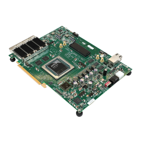
- Page 1 VCU128 Evaluation Board User Guide UG1302 (v1.1) April 21, 2021...
-
Page 2: Table Of Contents
Chapter 3: Board Component Descriptions ........... 18 Overview.............................18 Component Descriptions......................18 Appendix A: VITA 57.4 FMCP Connector Pinouts ......... 93 Overview.............................93 Appendix B: Xilinx Constraints File ..............94 Overview.............................94 Appendix C: Regulatory and Compliance Information ......95 Overview.............................95 CE Directives..........................95 CE Standards.......................... - Page 3 Xilinx Resources.........................97 Documentation Navigator and Design Hubs.................97 References..........................98 Please Read: Important Legal Notices................. 100 UG1302 (v1.1) April 21, 2021 www.xilinx.com Send Feedback VCU128 Board User Guide...
-
Page 4: Revision History
Revision Summary 04/21/2021 Version 1.1 Board Power System Revised the Renesas smart power stage module part number in the power system block diagram. 12/21/2018 Version 1.0 Initial release. UG1302 (v1.1) April 21, 2021 www.xilinx.com Send Feedback VCU128 Board User Guide... -
Page 5: Chapter 1: Introduction
(SSI) technology to add HBM die next to the FPGA die on the ® ® package substrate. The VCU128 evaluation board for the Xilinx Virtex UltraScale+™ FPGA provides a hardware environment for developing and evaluating designs targeting the UltraScale+ XCVU37P-2FSVH2892E device. -
Page 6: Block Diagram
• Virtex ® UltraScale+™ XCVU37P-2FSVH2892E device • Zynq ® -7000 SoC XC7Z010 based system controller • 4.5 GB DDR4 72-bit component memory interface (4.5 x [512 Mb x 16]) UG1302 (v1.1) April 21, 2021 www.xilinx.com Send Feedback VCU128 Board User Guide... - Page 7 Gen3 (x1, x2, x4, x8, x16) ○ Dual Gen4 (x1, x2, x4, x8) ○ • Ethernet PHY SGMII interface with RJ-45 connector • Dual USB-to-UART bridge with micro-B USB connector (shared FTDI FT4232HL) UG1302 (v1.1) April 21, 2021 www.xilinx.com Send Feedback VCU128 Board User Guide...
-
Page 8: Board Specifications
IMPORTANT! The VCU128 board height exceeds the standard 4.376-inch (11.15 cm) height of a PCI Express ® card. Environmental Temperature Operating: 0°C to +45°C, Storage: -25°C to +60°C Humidity 10% to 90% non-condensing Operating Voltage +12 VDC UG1302 (v1.1) April 21, 2021 www.xilinx.com Send Feedback VCU128 Board User Guide... -
Page 9: Chapter 2: Board Setup And Configuration
Before you pick it up again, touch the antistatic bag and the metal frame of the system at the same time. • Handle the devices carefully to prevent permanent damage. UG1302 (v1.1) April 21, 2021 www.xilinx.com Send Feedback VCU128 Board User Guide... -
Page 10: Board Component Location
Round callout references a component Square callout references a component on the front side of the board on the back side of the board 34 34 20 20 X22144-121718 UG1302 (v1.1) April 21, 2021 www.xilinx.com Send Feedback VCU128 Board User Guide... - Page 11 Four 28 Gb/s zQSFP+ Module Connectors, 4 x TE 1551920-2 connectors with TE 2170745-2 38, 39 QSFP1-4 (J42), (J39), (J35), (J32) + 1x4 cage with heatsink ganged cage UG1302 (v1.1) April 21, 2021 www.xilinx.com Send Feedback VCU128 Board User Guide...
- Page 12 1x3 0.1-inch male header Sullins PBC36SAAN Jumpers, SYS CTLR RE-PROG header, (J43) 1x2 0.1-inch male header Sullins PBC36SAAN The VCU128 board schematics are available for download from the VCU128 Evaluation Kit website. UG1302 (v1.1) April 21, 2021 www.xilinx.com Send Feedback VCU128 Board User Guide...
-
Page 13: Default Switch And Jumper Settings
1-2: 0.85V; 2-3: 0.72V PCIe ® lane size select 16-lane configuration SYSCTLR RE-PROG U42 XCZU7010 MIO5 pin Notes: VCCINT select header J25 should always have a jumper block installed. UG1302 (v1.1) April 21, 2021 www.xilinx.com Send Feedback VCU128 Board User Guide... -
Page 14: Installing The Board In A Pc Chassis
(use one cable or the other). • The ATX power supply 4-pin (1x4) peripheral connector, which requires using the ATX adapter cable (see the following figure) to connect to J16 on the VCU128 board. The Xilinx part number for this cable is 2600304. See ATX Power Supply Adapter Cable. - Page 15 J16 damages the VCU128 evaluation board and voids the board warranty. c. Slide the VCU128 board power switch SW5 to the ON position. The PC can now be powered on. UG1302 (v1.1) April 21, 2021 www.xilinx.com Send Feedback VCU128 Board User Guide...
-
Page 16: Fpga Configuration
• JTAG using: USB JTAG configuration port (U8 FT4232HL + USB J2 micro-AB) ○ Xilinx Platform Cable USB II, 2 mm, keyed flat cable header (J4) ○ Each configuration interface corresponds to one or more configuration modes and bus widths, as listed in the following table. - Page 17 ® The Vivado , Xilinx SDK, or third-party tools can establish a JTAG connection to the XCVU37P FPGA through the FTDI FT4232 USB-to-JTAG/USB UART device (U8) connected to the micro- USB connector (J2). Alternatively, a JTAG cable can be connected to the keyed flat cable header (J4).
-
Page 18: Chapter 3: Board Component Descriptions
Encryption Key Battery Backup Circuit The XCVU37P device U1 implements bitstream encryption key technology. The VCU128 board provides the encryption key backup battery circuit shown in the following figure. UG1302 (v1.1) April 21, 2021 www.xilinx.com Send Feedback VCU128 Board User Guide... - Page 19 HP bank 66 DDR4_VDDQ_1V2 1.2V HP bank 67 VCC1V8 1.8V HP bank 68 QDR4_VDDQ_1V2 1.2V HP bank 69 QDR4_VDDQ_1V2 1.2V HP bank 70 QDR4_VDDQ_1V2 1.2V HP bank 71 VADJ 1.8V UG1302 (v1.1) April 21, 2021 www.xilinx.com Send Feedback VCU128 Board User Guide...
- Page 20 XDC set_property INTERNAL VREF constraint, invoke the INTERNAL VREF mode. The connections between the 72-bit interface DDR4 component memories and XCVU37P banks 64, 65, and 66 are listed in the following table. UG1302 (v1.1) April 21, 2021 www.xilinx.com Send Feedback VCU128 Board User Guide...
- Page 21 POD12_DCI BH46 PL_DDR4_DQS2_T DIFF_POD12_DCI LDQS_T BJ46 PL_DDR4_DQS2_C DIFF_POD12_DCI LDQS_C BH42 PL_DDR4_DM2_B POD12_DCI NF/LDM_B/LDBI_B BE43 PL_DDR4_DQ24 POD12_DCI BF42 PL_DDR4_DQ25 POD12_DCI BC42 PL_DDR4_DQ26 POD12_DCI BF43 PL_DDR4_DQ27 POD12_DCI BD42 PL_DDR4_DQ28 POD12_DCI UG1302 (v1.1) April 21, 2021 www.xilinx.com Send Feedback VCU128 Board User Guide...
- Page 22 BH35 PL_DDR4_DQ51 POD12_DCI DQ11 BJ33 PL_DDR4_DQ52 POD12_DCI DQ12 BF35 PL_DDR4_DQ53 POD12_DCI DQ13 BG34 PL_DDR4_DQ54 POD12_DCI DQ14 BF36 PL_DDR4_DQ55 POD12_DCI DQ15 BK34 PL_DDR4_DQS6_T DIFF_POD12_DCI UDQS_T BK35 PL_DDR4_DQS6_C DIFF_POD12_DCI UDQS_C UG1302 (v1.1) April 21, 2021 www.xilinx.com Send Feedback VCU128 Board User Guide...
- Page 23 U17-U19 U73-U74 BG47 PL_DDR4_A9 SSTL12_DCI U17-U19 U73-U74 BF47 PL_DDR4_A10 SSTL12_DCI A10/AP U17-U19 U73-U74 BG49 PL_DDR4_A11 SSTL12_DCI U17-U19 U73-U74 BF48 PL_DDR4_A12 SSTL12_DCI A12/BC_B U17-U19 U73-U74 BF52 PL_DDR4_A13 SSTL12_DCI U17-U19 U73-U74 UG1302 (v1.1) April 21, 2021 www.xilinx.com Send Feedback VCU128 Board User Guide...
- Page 24 The 288 MB RLD3 72-bit wide component memory system is comprised of two 36-bit 1.125 Gb RLDRAM3 devices located at U39 and U37. • Manufacturer: Micron • Part Number: MT44K32M36RB-107E • Description: 1.125 Gb (32 Mb x 36) ○ UG1302 (v1.1) April 21, 2021 www.xilinx.com Send Feedback VCU128 Board User Guide...
- Page 25 DQ16 RLD3_72B_DQ17 SSTL12 DQ17 RLD3_72B_DQ18 SSTL12 DQ18 RLD3_72B_DQ19 SSTL12 DQ19 RLD3_72B_DQ20 SSTL12 DQ20 RLD3_72B_DQ21 SSTL12 DQ21 RLD3_72B_DQ22 SSTL12 DQ22 RLD3_72B_DQ23 SSTL12 DQ23 RLD3_72B_DQ24 SSTL12 DQ24 RLD3_72B_DQ25 SSTL12 DQ25 UG1302 (v1.1) April 21, 2021 www.xilinx.com Send Feedback VCU128 Board User Guide...
- Page 26 DQ18 RLD3_72B_DQ55 SSTL12 DQ19 RLD3_72B_DQ56 SSTL12 DQ20 RLD3_72B_DQ57 SSTL12 DQ21 RLD3_72B_DQ58 SSTL12 DQ22 RLD3_72B_DQ59 SSTL12 DQ23 RLD3_72B_DQ60 SSTL12 DQ24 RLD3_72B_DQ61 SSTL12 DQ25 RLD3_72B_DQ62 SSTL12 DQ26 RLD3_72B_DQ63 SSTL12 DQ27 UG1302 (v1.1) April 21, 2021 www.xilinx.com Send Feedback VCU128 Board User Guide...
- Page 27 U37, U39 RLD3_72B_A20 SSTL12 NF_A20 U37, U39 RLD3_72B_BA0 SSTL12 U37, U39 RLD3_72B_BA1 SSTL12 U37, U39 RLD3_72B_BA2 SSTL12 U37, U39 RLD3_72B_BA3 SSTL12 U37, U39 RLD3_72B_WE_B SSTL12 WE_B U37, U39 UG1302 (v1.1) April 21, 2021 www.xilinx.com Send Feedback VCU128 Board User Guide...
- Page 28 "RLD3 Design Guidelines" section of the UltraScale Architecture-Based FPGAs Memory IP LogiCORE IP Product Guide (PG150). The VCU128 RLD3 memory component interface is a 40Ω impedance implementation. UG1302 (v1.1) April 21, 2021 www.xilinx.com Send Feedback VCU128 Board User Guide...
- Page 29 INTERNAL VREF constraint, invoke the INTERNAL VREF mode. The connections between the 72-bit interface QDR4 component memories and XCVU37P banks 68, 69, and 70 are listed in the following table. UG1302 (v1.1) April 21, 2021 www.xilinx.com Send Feedback VCU128 Board User Guide...
- Page 30 BJ13 QDR4_DQA26 DQA26 QDR4_DQA27 DQA27 BE10 QDR4_DQA28 DQA28 BG13 QDR4_DQA29 DQA29 BE11 QDR4_DQA30 DQA30 BF10 QDR4_DQA31 DQA31 BG12 QDR4_DQA32 DQA32 QDR4_DQA33 DQA33 BG10 QDR4_DQA34 DQA34 BF12 QDR4_DQA35 DQA35 UG1302 (v1.1) April 21, 2021 www.xilinx.com Send Feedback VCU128 Board User Guide...
- Page 31 QDR4_DQB8 DQB8 QDR4_DQB9 DQB9 QDR4_DQB10 DQB10 QDR4_DQB11 DQB11 QDR4_DQB12 DQB12 QDR4_DQB13 DQB13 QDR4_DQB14 DQB14 QDR4_DQB15 DQB15 QDR4_DQB16 DQB16 QDR4_DQB17 DQB17 QDR4_DQB18 DQB18 QDR4_DQB19 DQB19 QDR4_DQB20 DQB20 QDR4_DQB21 DQB21 UG1302 (v1.1) April 21, 2021 www.xilinx.com Send Feedback VCU128 Board User Guide...
- Page 32 QKB0_N QDR4_QKB1_P QKB1_P QDR4_QKB1_N QKB1_N QDR4_QVLDB0 QVLDB0 QDR4_QVLDB1 QVLDB1 QDR4_LDB_N LDB_N QDR4_RWB_N RWB_N R606(GND) QDR4_DINVB0 DINVB0 R602(GND) QDR4_DINVB1 DINVB1 Common QDR4_A0 QDR4_A1 QDR4_A2 QDR4_A3 QDR4_A4 QDR4_A5 QDR4_A6 QDR4_A7 UG1302 (v1.1) April 21, 2021 www.xilinx.com Send Feedback VCU128 Board User Guide...
- Page 33 “VREF”, and “Internal VREF” sections in the UltraScale Architecture SelectIO Resources User Guide (UG571). For more details about the Cypress QDR-IV component memory, see the Cypress CY7C4142KV13_106FCXC Data Sheet at the Cypress Semiconductor website. UG1302 (v1.1) April 21, 2021 www.xilinx.com Send Feedback VCU128 Board User Guide...
- Page 34 The Quad SPI circuitry is shown in the following figure. Figure 7: Quad SPI (2 Gbit) Flash Memory X21957-121918 The connections between the Quad SPI flash memory and the XCVU37P FPGA are listed in the following table. UG1302 (v1.1) April 21, 2021 www.xilinx.com Send Feedback VCU128 Board User Guide...
- Page 35 (U8) where a host computer accesses the VCU128 board JTAG chain through a type-A (PC host side) to micro-AB (VCU128 board side J2) USB cable. A 2 mm JTAG header (J4) is also provided in parallel for access by Xilinx ®...
- Page 36 JTAG chain connects to the FPGA U1. The JTAG connectivity on the VCU128 board allows a host computer to download bitstreams to the FPGA using the Xilinx tools. In addition, the JTAG connector allows debug tools such as the Vivado ®...
- Page 37 The USB UART interface circuit is shown in the following figure. The FTDI FT4232HL data sheet is available on the Future Technology Devices International Ltd. website. Figure 9: FTDI USB JTAG/UART Circuit X21958-121918 UG1302 (v1.1) April 21, 2021 www.xilinx.com Send Feedback VCU128 Board User Guide...
- Page 38 Table 11: Clock Sources to XCVU37P FPGA U1 Connections Clock Source Device/ Schematic Net Name I/O Standard FPGA (U1) Pin U#.Pin# Memory Interface Clocks SIT9120AI/U76.4 DDR4_CLK_100MHZ_P LVDS BH51 SIT9120AI/U76.5 DDR4_CLK_100MHZ_N LVDS BJ51 SIT9120AI/U96.4 QDR4_CLK_100MHZ_P LVDS UG1302 (v1.1) April 21, 2021 www.xilinx.com Send Feedback VCU128 Board User Guide...
- Page 39 SI5328B/U87.34 SI5328_CLOCK2_P Notes: Series capacitor coupled, MGT connections I/O standard is not applicable. Signal amplitude not to exceed FPGA U1 bank 67 VCCO = VCC1V8 rail = 1.8V. UG1302 (v1.1) April 21, 2021 www.xilinx.com Send Feedback VCU128 Board User Guide...
- Page 40 • 0.6 ps RMS phase jitter (random) over 12 kHz to 20 MHz bandwidth • 3.3V LVDS differential output The DDR4 interface fixed frequency clock circuit is shown in the following figure. Figure 10: DDR4 Interface Clock X21959-121918 UG1302 (v1.1) April 21, 2021 www.xilinx.com Send Feedback VCU128 Board User Guide...
- Page 41 • 0.6 ps RMS phase jitter (random) over 12 kHz to 20 MHz bandwidth • 3.3V LVDS differential output The QDR4 interface fixed frequency clock circuit is shown in the following figure. Figure 11: QDR4 Interface Clock X21961-111918 UG1302 (v1.1) April 21, 2021 www.xilinx.com Send Feedback VCU128 Board User Guide...
- Page 42 The RLD3 interface fixed frequency clock circuit is shown in the following figure. The SiTime SiT9120AI data sheet is available on the SiTime Corp. website. Figure 12: RLD3 Interface Clock X21962-111918 UG1302 (v1.1) April 21, 2021 www.xilinx.com Send Feedback VCU128 Board User Guide...
- Page 43 • Programmable oscillator: Silicon Labs Si570BAB0000544DG (10 MHz-810 MHz) • Frequency tolerance: 50 ppm • 3.3V LVDS differential output The programmable QSFP1 clock circuit is shown in the following figure. Figure 13: QSFP1 Clock X21963-121918 UG1302 (v1.1) April 21, 2021 www.xilinx.com Send Feedback VCU128 Board User Guide...
- Page 44 • Programmable oscillator: Silicon Labs Si570BAB0000544DG (10 MHz-810 MHz) • Frequency tolerance: 50 ppm • 3.3V LVDS differential output The programmable QSFP2 clock circuit is shown in the following figure. Figure 14: QSFP2 Clock X21964-121918 UG1302 (v1.1) April 21, 2021 www.xilinx.com Send Feedback VCU128 Board User Guide...
- Page 45 • Programmable oscillator: Silicon Labs Si570BAB0000544DG (10 MHz-810 MHz) • Frequency tolerance: 50 ppm • 3.3V LVDS differential output The programmable QSFP3 clock circuit is shown in the following figure. Figure 15: QSFP3 Clock X21965-111918 UG1302 (v1.1) April 21, 2021 www.xilinx.com Send Feedback VCU128 Board User Guide...
- Page 46 • Programmable oscillator: Silicon Labs Si570BAB0000544DG (10 MHz-810 MHz) • Frequency tolerance: 50 ppm • 3.3V LVDS differential output The programmable QSFP4 clock circuit is shown in the following figure. Figure 16: QSFP4 Clock X21966-121918 UG1302 (v1.1) April 21, 2021 www.xilinx.com Send Feedback VCU128 Board User Guide...
- Page 47 –0.5V min. to 1.3V max. The user SMA MGT clock circuit is shown in the following figure. Figure 17: QSFP SMA Clock X21967-121918 UG1302 (v1.1) April 21, 2021 www.xilinx.com Send Feedback VCU128 Board User Guide...
- Page 48 SMA_CLK_OUTPUT SMA connectors in input mode must be equal to or less than the VCCO for bank 67. This value must be confirmed prior to applying signals to the SMA_CLK_OUTPUT connectors. Figure 18: User SMA Clock X22055-121918 UG1302 (v1.1) April 21, 2021 www.xilinx.com Send Feedback VCU128 Board User Guide...
- Page 49 GTY transceiver. The jitter attenuated clock circuit is shown in the following figure. Figure 19: QSFP Recovery Clock X21968-121918 UG1302 (v1.1) April 21, 2021 www.xilinx.com Send Feedback VCU128 Board User Guide...
- Page 50 • Four GTY transceivers allocated to QSFP1_TX/RX[1:4]_P/N Quad 134 • MGTREFCLK0 – QSFP2_SI570_CLOCK_P/N • MGTREFCLK1 – SI5328_CLOCK1_C_P/N • Four GTY transceivers allocated to QSFP2_TX/RX[1:4]_P/N Quad 132 • MGTREFCLK0 – QSFP3_SI570_CLOCK_P/N UG1302 (v1.1) April 21, 2021 www.xilinx.com Send Feedback VCU128 Board User Guide...
- Page 51 • Four GTY transceivers allocated to FMCP_HSPC_DP[8:11] Quad 125 • MGTREFCLK0 – FMCP_HSPC_GBTCLK1_M2C_P/N • NC • Four GTY transceivers allocated to FMCP_HSPC_DP[4:7] Quad 124 • MGTREFCLK0 – FMCP_HSPC_GBTCLK0_M2C_P/N • NC UG1302 (v1.1) April 21, 2021 www.xilinx.com Send Feedback VCU128 Board User Guide...
- Page 52 FMCP_HSPC_DP23 FMCP_HSPC_DP3 MGTY_129_REFCLK0 MGTY_124_REFCLK0 FMCP_HSPC_GBTCLK5_M2C FMCP_HSPC_GBTCLK0_M2C MGTY_129_REFCLK1 MGTY_124_REFCLK1 X21650-092618 Right-side GTY Transceiver Connectivity The following tables list the connectivity of the ten XCVU37P FPGA U1 right-side GTY transceivers. UG1302 (v1.1) April 21, 2021 www.xilinx.com Send Feedback VCU128 Board User Guide...
- Page 53 TX4P MGTYTXN3_135 QSFP1_TX4_N TX4N MGTYRXP3_135 QSFP1_RX4_P RX4P MGTYRXN3_135 QSFP1_RX4_N RX4N MGTREFCLK0P_135 QSFP_SI570_CLOCK_P U95 SI570 I2C prog. osc. MGTREFCLK0N_135 QSFP_SI570_CLOCK_N OUT_B MGTREFCLK1P_135 MGTREFCLK1N_135 Notes: Series 0.01 µF capacitor coupled. UG1302 (v1.1) April 21, 2021 www.xilinx.com Send Feedback VCU128 Board User Guide...
- Page 54 QSFP2_RX4_N RX4N MGTREFCLK0P_134 QSFP2_SI570_CLOCK_P U90 SI570 I2C prog. osc. MGTREFCLK0N_134 QSFP2_SI570_CLOCK_N OUT_B MGTREFCLK1P_134 SI5328_CLOCK1_C_P CKOUT1_P U87 SI5328B jitter atten. MGTREFCLK1N_134 SI5328_CLOCK1_C_N CKOUT1_N Notes: Series 0.01 µF capacitor coupled. UG1302 (v1.1) April 21, 2021 www.xilinx.com Send Feedback VCU128 Board User Guide...
- Page 55 QSFP3_RX4_N RX4N MGTREFCLK0P_132 QSFP3_SI570_CLOCK_P U82 SI570 I2C prog. osc. MGTREFCLK0N_132 QSFP3_SI570_CLOCK_N OUT_B MGTREFCLK1P_132 SI5328_CLOCK2_C_P CKOUT2_P U87 SI5328B jitter atten. MGTREFCLK1N_132 SI5328_CLOCK2_C_N CKOUT2_N Notes: Series 0.01 µF capacitor coupled. UG1302 (v1.1) April 21, 2021 www.xilinx.com Send Feedback VCU128 Board User Guide...
- Page 56 QSFP4_SI570_CLOCK_P U80 SI570 I2C prog. osc. AB43 MGTREFCLK0N_131 QSFP4_SI570_CLOCK_N OUT_B AA40 MGTREFCLK1P_131 SMA_REFCLK_INPUT_P SMA J24 (P) SMA J26 (N) AA41 MGTREFCLK1N_131 SMA_REFCLK_INPUT_N Notes: Series 0.01 µF capacitor coupled. UG1302 (v1.1) April 21, 2021 www.xilinx.com Send Feedback VCU128 Board User Guide...
- Page 57 FMCP_HSPC_DP23_C2M_N DP23_C2M_N AE49 MGTYRXP3_129 FMCP_HSPC_DP23_M2C_P DP23_M2C_P AE50 MGTYRXN3_129 FMCP_HSPC_DP23_M2C_N DP23_M2C_N AG40 MGTREFCLK0P_129 FMCP_HSPC_GBTCLK5_M2C_P GBTCLK5_M2C_P AG41 MGTREFCLK0N_129 FMCP_HSPC_GBTCLK5_M2C_N GBTCLK5_M2C_N AF42 MGTREFCLK1P_129 AF43 MGTREFCLK1N_129 Notes: Series 0.01 µF capacitor coupled. UG1302 (v1.1) April 21, 2021 www.xilinx.com Send Feedback VCU128 Board User Guide...
- Page 58 FMCP_HSPC_DP19_C2M_N DP19_C2M_N AH51 MGTYRXP3_128 FMCP_HSPC_DP19_M2C_P DP19_M2C_P AH52 MGTYRXN3_128 FMCP_HSPC_DP19_M2C_N DP19_M2C_N AJ40 MGTREFCLK0P_128 FMCP_HSPC_GBTCLK4_M2C_P GBTCLK4_M2C_P AJ41 MGTREFCLK0N_128 FMCP_HSPC_GBTCLK4_M2C_N GBTCLK4_M2C_N AH42 MGTREFCLK1P_128 AH43 MGTREFCLK1N_128 Notes: Series 0.01 µF capacitor coupled. UG1302 (v1.1) April 21, 2021 www.xilinx.com Send Feedback VCU128 Board User Guide...
- Page 59 FMCP_HSPC_DP15_C2M_N DP15_C2M_N AL53 MGTYRXP3_127 FMCP_HSPC_DP15_M2C_P DP15_M2C_P AL54 MGTYRXN3_127 FMCP_HSPC_DP15_M2C_N DP15_M2C_N AL40 MGTREFCLK0P_127 FMCP_HSPC_GBTCLK3_M2C_P GBTCLK3_M2C_P AL41 MGTREFCLK0N_127 FMCP_HSPC_GBTCLK3_M2C_N GBTCLK3_M2C_N AK42 MGTREFCLK1P_127 AK43 MGTREFCLK1N_127 Notes: Series 0.01 µF capacitor coupled. UG1302 (v1.1) April 21, 2021 www.xilinx.com Send Feedback VCU128 Board User Guide...
- Page 60 FMCP_HSPC_DP11_C2M_N DP11_C2M_N AP51 MGTYRXP3_126 FMCP_HSPC_DP11_M2C_P DP11_M2C_P AP52 MGTYRXN3_126 FMCP_HSPC_DP11_M2C_N DP11_M2C_N AN40 MGTREFCLK0P_126 FMCP_HSPC_GBTCLK2_M2C_P GBTCLK2_M2C_P AN41 MGTREFCLK0N_126 FMCP_HSPC_GBTCLK2_M2C_N1 GBTCLK2_M2C_N AM42 MGTREFCLK1P_126 AM43 MGTREFCLK1N_126 Notes: Series 0.01 µF capacitor coupled. UG1302 (v1.1) April 21, 2021 www.xilinx.com Send Feedback VCU128 Board User Guide...
- Page 61 FMCP_HSPC_DP7_C2M_N DP7_C2M_N AV51 MGTYRXP3_125 FMCP_HSPC_DP7_M2C_P DP7_M2C_P AV52 MGTYRXN3_125 FMCP_HSPC_DP7_M2C_N DP7_M2C_N AR40 MGTREFCLK0P_125 FMCP_HSPC_GBTCLK1_M2C_P GBTCLK1_M2C_P AR41 MGTREFCLK0N_125 FMCP_HSPC_GBTCLK1_M2C_N GBTCLK1_M2C_N AP42 MGTREFCLK1P_125 AP43 MGTREFCLK1N_125 Notes: Series 0.01 µF capacitor coupled. UG1302 (v1.1) April 21, 2021 www.xilinx.com Send Feedback VCU128 Board User Guide...
- Page 62 MGTREFCLK1 - not connected ○ Four GTY transceivers allocated to PCIe lanes 3:0 PCIE_EP_TX/RX[3:0] ○ • Quad 226 MGTREFCLK0 - not connected ○ MGTREFCLK1 - not connected ○ UG1302 (v1.1) April 21, 2021 www.xilinx.com Send Feedback VCU128 Board User Guide...
- Page 63 (PG182). For additional information about the quad small form factor pluggable (28 Gb/s QSFP28) module, see the SFF-8663 and SFF-8679 specifications for the 28 Gb/s QSFP+ at the SNIA Technology Affiliates website. UG1302 (v1.1) April 21, 2021 www.xilinx.com Send Feedback VCU128 Board User Guide...
- Page 64 PCIE_EP_TX0_N PERN0 MGTYRXP3_227 PCIE_EP_RX0_P PETP0 MGTYRXN3_227 PCIE_EP_RX0_N PETN0 AL15 MGTREFCLK0P_227 PCIE_CLK2_P ICS85411A U94 clock AL14 MGTREFCLK0N_227 PCIE_CLK2_N buffer AK13 MGTREFCLK1P_227 AK12 MGTREFCLK1N_227 Notes: Series 0.01 µF capacitor coupled. UG1302 (v1.1) April 21, 2021 www.xilinx.com Send Feedback VCU128 Board User Guide...
- Page 65 AR11 MGTYTXP3_226 PCIE_EP_TX4_P PERP4 AR10 MGTYTXN3_226 PCIE_EP_TX4_N PERN4 MGTYRXP3_226 PCIE_EP_RX4_P PETP4 MGTYRXN3_226 PCIE_EP_RX4_N PETN4 AN15 MGTREFCLK0P_226 AN14 MGTREFCLK0N_226 AM13 MGTREFCLK1P_226 AM12 MGTREFCLK1N_226 Notes: Series 0.01 µF capacitor coupled. UG1302 (v1.1) April 21, 2021 www.xilinx.com Send Feedback VCU128 Board User Guide...
- Page 66 PCIE_EP_TX8_N PERN8 MGTYRXP3_225 PCIE_EP_RX8_P PETP8 MGTYRXN3_225 PCIE_EP_RX8_N PETN8 AR15 MGTREFCLK0P_225 PCIE_CLK1_P ICS85411A U94 clock AR14 MGTREFCLK0N_225 PCIE_CLK1_N buffer AP13 MGTREFCLK1P_225 AP12 MGTREFCLK1N_225 Notes: Series 0.01 µF capacitor coupled. UG1302 (v1.1) April 21, 2021 www.xilinx.com Send Feedback VCU128 Board User Guide...
- Page 67 Gen4 applications. The PCIe ® transmit and receive signal data paths have a characteristic impedance of 85Ω ±10%. The PCIe clock is routed as a 100Ω differential pair. UG1302 (v1.1) April 21, 2021 www.xilinx.com Send Feedback VCU128 Board User Guide...
- Page 68 For additional information about UltraScale™ PCIe functionality, see the UltraScale Devices Gen3 Integrated Block for PCI Express LogiCORE IP Product Guide (PG156). Additional information about the PCI Express standard is available on the PCI Express standard website. UG1302 (v1.1) April 21, 2021 www.xilinx.com Send Feedback VCU128 Board User Guide...
- Page 69 QSFP28 connections to the XCVU37P FPGA U1 MGTY transceiver banks 135 (QSFP1), 134 (QSFP2), 132 (QSFP3), and 131 (QSFP4). Figure 23: 28 Gb/s QSFP28 Module Connector X21970-112818 UG1302 (v1.1) April 21, 2021 www.xilinx.com Send Feedback VCU128 Board User Guide...
- Page 70 QSFP4 J32 (U1 bank 67) BK23 QSFP4_MODSKLL_LS Output MODSELL BK24 QSFP4_RESETL_LS Output RESETL BL22 QSFP4_MODPRSL_LS Output MODPRSL BH21 QSFP4_INTL_LS Input INTL BH21 QSFP4_LPMODE_LS Output LPMODE U54.19 QSFP4_I2C_SDA BiDir UG1302 (v1.1) April 21, 2021 www.xilinx.com Send Feedback VCU128 Board User Guide...
- Page 71 TX_D0_SGMII_SIN BJ21 ENET_SGMII_OUT_N LVCMOS18 RX_D3_SGMII_SON BH21 ENET_SGMII_OUT_P LVCMOS18 RX_D2_SGMII_SOP BK22 ENET_SGMII_CLK_N LVCMOS18 RX_D1_SGMII_CON BK23 ENET_SGMII_CLK_P LVCMOS18 RX_D0_SGMII_COP U65.10 GEM3_ENET_RESET_B RESET_B BP27 ENET_COL_GPIO LVCMOS18 GPIO_2 BJ23 ENET_CLKOUT LVCMOS18 CLK_OUT UG1302 (v1.1) April 21, 2021 www.xilinx.com Send Feedback VCU128 Board User Guide...
- Page 72 1-to-8 channel TI TCA9548A bus switches U53 (address 0x74) and U54 (address 0x76). The bus switches can operate at speeds up to 400 kHz. The VCU128 evaluation board I2C0 I2C bus topology is shown in the following figures. UG1302 (v1.1) April 21, 2021 www.xilinx.com Send Feedback VCU128 Board User Guide...
- Page 73 I2C0 U55 PCA9544A, address 0x75 (0b111101); U53 TCA9548A, address 0x74 (0b1110100), or U54 TCA9548A, address 0x76 (0b111110), respectively. The following table lists the address for each bus. UG1302 (v1.1) April 21, 2021 www.xilinx.com Send Feedback VCU128 Board User Guide...
- Page 74 0b1010000 0x50 QSFP4 module J32 28 Gb/s QSFP+ 0b1010000 0x50 Notes: Onboard Power System Devices. Information about the PCA9544A, TCA9548, and TCA6416A is available on the Semiconductor website. UG1302 (v1.1) April 21, 2021 www.xilinx.com Send Feedback VCU128 Board User Guide...
- Page 75 SYSTEM CTLR error (red) DS17 SYSTEM CTLR status DS18 SYSTEM CTLR done DS19 ENET PHY link DS20 12V On EPHY P2 RT ENET LINK1000 EPHY P2 LFT ENET link activity UG1302 (v1.1) April 21, 2021 www.xilinx.com Send Feedback VCU128 Board User Guide...
- Page 76 ○ The following figure shows the GPIO circuits. Figure 26: User GPIO X21972-112918 GPIO Connections to FPGA U1 The following table lists the GPIO connections to FPGA U1. UG1302 (v1.1) April 21, 2021 www.xilinx.com Send Feedback VCU128 Board User Guide...
- Page 77 VCU128 board power switch is on. See Board Power System for details on the onboard power system. The following figure shows the power connector J16, power switch SW5, and indicator LED DS20. UG1302 (v1.1) April 21, 2021 www.xilinx.com Send Feedback VCU128 Board User Guide...
- Page 78 FPGA configuration. The FPGA_PROG_B signal is connected to XCVU37P FPGA U1 pin BB15. See the UltraScale Architecture Configuration User Guide (UG570) for further configuration details. The following figure shows SW2. UG1302 (v1.1) April 21, 2021 www.xilinx.com Send Feedback VCU128 Board User Guide...
- Page 79 • The 560-pin FMC+ connector defined by the FMC specification (see Appendix A: VITA 57.4 FMCP Connector Pinouts) provides connectivity for up to: 160 single-ended or 80 differential user-defined signals ○ UG1302 (v1.1) April 21, 2021 www.xilinx.com Send Feedback VCU128 Board User Guide...
- Page 80 • 68 single-ended or 34 differential user-defined pairs (full LA-bus: LA[00:33]) • 24 transceiver differential pairs • 6 transceiver differential clocks • 2 differential clocks • 239 ground and 14 power connections UG1302 (v1.1) April 21, 2021 www.xilinx.com Send Feedback VCU128 Board User Guide...
- Page 81 AU49 FMCP_HSPC_DP3_C2M_N LVDS BA45 FMCP_HSPC_DP7_C2M_P LVDS AU44 FMCP_HSPC_DP4_C2M_P LVDS AY46 FMCP_HSPC_DP7_C2M_N LVDS AU45 FMCP_HSPC_DP4_C2M_N LVDS AY47 FMCP_HSPC_DP6_C2M_P LVDS AV46 FMCP_HSPC_DP5_C2M_P LVDS AW44 FMCP_HSPC_DP6_C2M_N LVDS AV47 FMCP_HSPC_DP5_C2M_N LVDS AW45 UG1302 (v1.1) April 21, 2021 www.xilinx.com Send Feedback VCU128 Board User Guide...
- Page 82 FMCP_HSPC_LA23_N LVDS FMCP_HSPC_IIC_SDA FMCP_HSPC_LA26_P LVDS GA0 = 0 = GND FMCP_HSPC_LA26_N LVDS VCC12_SW FMCP_HSPC_TCK_BUF VCC12_SW FPGA_TDO_FMC_TDI_BUF UTIL_3V3 FMCP_HSPC_TDO_HPC1_TDI UTIL_3V3 FMCP_HSPC_TMS_BUF GA1 = 0 = GND UTIL_3V3 UTIL_3V3 UTIL_3V3 UG1302 (v1.1) April 21, 2021 www.xilinx.com Send Feedback VCU128 Board User Guide...
- Page 83 FMCP_HSPC_LA24_P LVDS FMCP_HSPC_LA29_N LVDS FMCP_HSPC_LA24_N LVDS FMCP_HSPC_LA31_P LVDS FMCP_HSPC_LA28_P LVDS FMCP_HSPC_LA31_N LVDS FMCP_HSPC_LA28_N LVDS FMCP_HSPC_LA33_P LVDS FMCP_HSPC_LA30_P LVDS FMCP_HSPC_LA33_N LVDS FMCP_HSPC_LA30_N LVDS VADJ_1V8_FPGA FMCP_HSPC_LA32_P LVDS FMCP_HSPC_LA32_N LVDS VADJ UG1302 (v1.1) April 21, 2021 www.xilinx.com Send Feedback VCU128 Board User Guide...
- Page 84 FMCP_HSPC_SYNC_M2C_P LVDS FMCP_HSPC_DP16_C2M_N LVDS AK47 FMCP_HSPC_SYNC_M2C_N LVDS FMCP_HSPC_DP17_C2M_P LVDS AJ48 FMCP_HSPC_DP17_C2M_N LVDS AJ49 FMCP_HSPC_DP18_C2M_P LVDS AJ44 VCC12_SW FMCP_HSPC_DP18_C2M_N LVDS AJ45 VCC12_SW FMCP_HSPC_DP19_C2M_P LVDS AH46 VCC12_SW FMCP_HSPC_DP19_C2M_N LVDS AH47 UG1302 (v1.1) April 21, 2021 www.xilinx.com Send Feedback VCU128 Board User Guide...
- Page 85 Marketing Alliance website. Board Power System [Figure 2, callout 34] The VCU128 board has an Intersil power system. The following figure shows the VCU128 board power system block diagram. UG1302 (v1.1) April 21, 2021 www.xilinx.com Send Feedback VCU128 Board User Guide...
- Page 86 1.2V @ 20A ISL68301 + ISL99227B 103W Current Shunt VCCINT 0.85V @ 125A ISL68127 + ISL919227 (5) Current Shunt VCCBRAM 0.85V @ 30A ISL68127 + ISL919227 (1) X21654-040821 UG1302 (v1.1) April 21, 2021 www.xilinx.com Send Feedback VCU128 Board User Guide...
- Page 87 Documentation describing the programming of the Intersil power controllers is available on the Intersil website (see References). The PCB layout and power system design meet the recommended criteria described in the UltraScale Architecture PCB Design User Guide (UG583). UG1302 (v1.1) April 21, 2021 www.xilinx.com Send Feedback VCU128 Board User Guide...
- Page 88 Programmable Regulators and INA226 Map Programmable Regulators VCCINT (PWM[2:6]) ISL68127IRAZ-TR5823 0.72 - 0X65 0x40 0.85 VCCBRAM (PWM[0]) ISL68127IRAZ-TR5823 0.72 - 0X65 0x41 0.85 VCC1V8 (PH_A/B) ISL91302BIKZ-TR5814 4 - 6 0x63 0X42 UG1302 (v1.1) April 21, 2021 www.xilinx.com Send Feedback VCU128 Board User Guide...
- Page 89 DXP and DXN. The fan circuit is set up to increase fan speed as the FPGA temperature increases. Note: At initial power on, it is normal for the fan controller to energize at full speed for a few seconds. UG1302 (v1.1) April 21, 2021 www.xilinx.com Send Feedback VCU128 Board User Guide...
- Page 90 3. Connect the micro-B USB cable between the VCU128 board USB-UART connector (J2) and the host PC. 4. Power-cycle the VCU128 board. 5. Launch the SCUI as shown in the following example. UG1302 (v1.1) April 21, 2021 www.xilinx.com Send Feedback VCU128 Board User Guide...
- Page 91 • Master SPI using the onboard 2 Gbit Quad SPI flash memory • JTAG using: USB JTAG configuration port J2 (FTDI FT4232H bridge U8) ○ Xilinx ® platform cable 2 mm, keyed flat cable header (J4) ○ Each configuration interface corresponds to one or more configuration modes and bus widths as listed in the following table.
- Page 92 FPGA. DIP switch SW1 also includes a system controller enable switch in position 1. See the UltraScale Architecture Configuration User Guide (UG570) for further details on configuration modes. UG1302 (v1.1) April 21, 2021 www.xilinx.com Send Feedback VCU128 Board User Guide...
-
Page 93: Appendix A: Vita 57.4 Fmcp Connector Pinouts
VITA 57.4 FMC specification. For a description of how the VCU128 evaluation board implements the FMCP specification, see FPGA Mezzanine Card Interface. Figure 32: FMCP Connector Pinouts X21978-112818 UG1302 (v1.1) April 21, 2021 www.xilinx.com Send Feedback VCU128 Board User Guide... -
Page 94: Appendix B: Xilinx Constraints File
Appendix B: Xilinx Constraints File Appendix B Xilinx Constraints File Overview The Xilinx ® design constraints (XDC) file template for the VCU128 board provides for designs targeting the VCU128 evaluation board. Net names in the constraints listed correlate with net names on the latest VCU128 evaluation board schematic. -
Page 95: Appendix C: Regulatory And Compliance Information
Electromagnetic Compatibility EN 55022:2010, Information Technology Equipment Radio Disturbance Characteristics – Limits and Methods of Measurement EN 55024:2010, Information Technology Equipment Immunity Characteristics – Limits and Methods of Measurement UG1302 (v1.1) April 21, 2021 www.xilinx.com Send Feedback VCU128 Board User Guide... -
Page 96: Compliance Markings
Xilinx has met its national obligations to the EU WEEE Directive by registering in those countries to which Xilinx is an importer. Xilinx has also elected to join WEEE Compliance Schemes in some countries to help manage customer returns at end-of-life. -
Page 97: Appendix D: Additional Resources And Legal Notices
• On Windows, select Start → All Programs → Xilinx Design Tools → DocNav. • At the Linux command prompt, enter docnav. Xilinx Design Hubs provide links to documentation organized by design tasks and other topics, which you can use to learn key concepts and address frequently asked questions. To access the Design Hubs: •... - Page 98 14. VCU128 System Controller Tutorial (XTP534) 15. VCU128 Software Install and Board Setup Tutorial (XTP535) 16. VCU128 Restoring Flash Tutorial (XTP533) 17. For additional documents associated with Xilinx devices, design tools, intellectual property, boards, and kits see the Xilinx documentation website.
- Page 99 ATX Power Supply Adapter Cable The Xilinx ATX cable part number 2600304 is manufactured by Sourcegate Technologies and is equivalent to the Sourcegate Technologies part number AZCBL-WH-11009. Sourcegate only manufactures the latest revision, which is currently A4. To order, contact Aries Ang, aries.ang@sourcegate.net, +65 6483 2878 for price and availability.
- Page 100 IP cores may be subject to warranty and support terms contained in a license issued to you by Xilinx. Xilinx products are not designed or intended to be fail-safe or for use in any application requiring fail-safe performance; you assume sole risk and liability for...
- Page 101 Mouser Electronics Authorized Distributor Click to View Pricing, Inventory, Delivery & Lifecycle Information: Xilinx EK-U1-VCU128-G EK-U1-VCU128-G-J EK-U1-VCU128-ES1-G-J EK-U1-VCU128-ES1-G...
Need help?
Do you have a question about the EK-U1-VCU128-G-J and is the answer not in the manual?
Questions and answers