
Related Manuals for Xilinx VC709


Summary of Contents for Xilinx VC709
- Page 1 VC709 Evaluation Board for the Virtex-7 FPGA User Guide UG887 (v1.0) February 4, 2013...
-
Page 2: Revision History
Limited Warranties which can be viewed at http://www.xilinx.com/warranty.htm; IP cores may be subject to warranty and support terms contained in a license issued to you by Xilinx. Xilinx products are not designed or intended to be fail-safe or for use in any application requiring fail-safe performance;... -
Page 3: Table Of Contents
VC709 Board Features ........ - Page 4 ..............96 www.xilinx.com VC709 Evaluation Board UG887 (v1.0) February 4, 2013...
-
Page 5: Chapter 1: Vc709 Evaluation Board Features
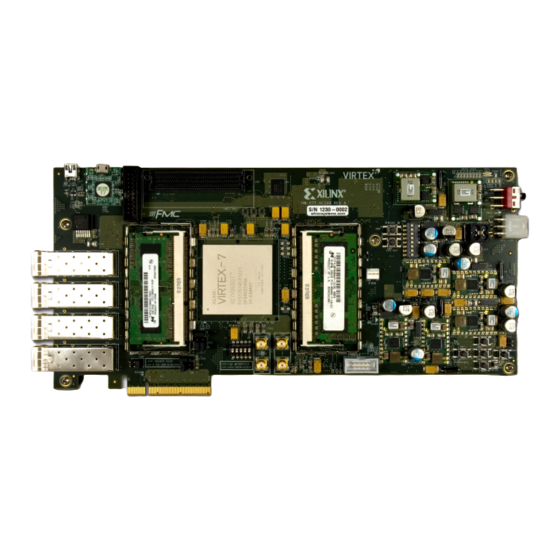
Chapter 1 VC709 Evaluation Board Features Overview The VC709 evaluation board for the Virtex®-7 FPGA provides a hardware environment for developing and evaluating designs targeting the Virtex-7 XC7VX690T-2FFG1761CES FPGA. The VC709 board provides features common to many embedded processing systems, including dual DDR3 small outline dual-inline memory module (SODIMM) memories, an 8-lane PCI Express®... - Page 6 USB JTAG (Digilent) configuration port The VC709 board block diagram is shown in Figure 1-1. Caution! The VC709 board can be damaged by electrostatic discharge (ESD). Follow standard ESD prevention measures when handling the board. www.xilinx.com VC709 Evaluation Board UG887 (v1.0) February 4, 2013...
-
Page 7: Feature Descriptions
C Bus Switch Flash Addr Connector UG887_c1_01_012113 Figure 1-1: VC709 Board Block Diagram Feature Descriptions Figure 1-2 shows the VC709 board. Each numbered feature that is referenced in Figure 1-2 is described in Table 1-1 and following sections. Note: The image in... - Page 8 Chapter 1: VC709 Evaluation Board Features X-Ref Target - Figure 1-2 Round callout references a component Square callout references a component on the front side of the board. on the back side of the board. UG887_c1_02_082612 Figure 1-2: VC709 Board Component Locations...
-
Page 9: Virtex-7 Xc7Vx690T-2Ffg1761Ces Fpga
Master BPI using the onboard linear BPI flash memory • JTAG using a type-A to micro-B USB cable for connecting the host PC to the VC709 board configuration port Each configuration interface corresponds to one or more configuration modes and bus... - Page 10 There are 17 I/O banks available on the Virtex-7 device. Fourteen I/O banks are available on the VC709 board, and banks 12, 16, and 18 are not used. The voltages applied to the FPGA I/O banks used by the VC709 board are listed in Table 1-3.
-
Page 11: Dual Ddr3 Memory Sodimms
Table 1-4: DDR3 SODIMM Socket J1 Connections to the FPGA SODIMM Memory J3 XCVX690T (U1) Pin Net Name Pin Number Pin Number DDR3_A_A0 DDR3_A_A1 DDR3_A_A2 DDR3_A_A3 DDR3_A_A4 DDR3_A_A5 DDR3_A_A6 DDR3_A_A7 DDR3_A_A8 DDR3_A_A9 DDR3_A_A10 A10/AP DDR3_A_A11 VC709 Evaluation Board www.xilinx.com UG887 (v1.0) February 4, 2013... - Page 12 Chapter 1: VC709 Evaluation Board Features Table 1-4: DDR3 SODIMM Socket J1 Connections to the FPGA (Cont’d) SODIMM Memory J3 XCVX690T (U1) Pin Net Name Pin Number Pin Number DDR3_A_A12 A12_BC_N DDR3_A_A13 DDR3_A_A14 DDR3_A_A15 DDR3_A_BA0 DDR3_A_BA1 DDR3_A_BA2 DDR3_A_D0 DDR3_A_D1 DDR3_A_D2...
- Page 13 DQ41 DDR3_A_D42 DQ42 DDR3_A_D43 DQ43 DDR3_A_D44 DQ44 DDR3_A_D45 DQ45 DDR3_A_D46 DQ46 DDR3_A_D47 DQ47 DDR3_A_D48 DQ48 DDR3_A_D49 DQ49 DDR3_A_D50 DQ50 DDR3_A_D51 DQ51 DDR3_A_D52 DQ52 DDR3_A_D53 DQ53 DDR3_A_D54 DQ54 DDR3_A_D55 DQ55 DDR3_A_D56 DQ56 VC709 Evaluation Board www.xilinx.com UG887 (v1.0) February 4, 2013...
- Page 14 Chapter 1: VC709 Evaluation Board Features Table 1-4: DDR3 SODIMM Socket J1 Connections to the FPGA (Cont’d) SODIMM Memory J3 XCVX690T (U1) Pin Net Name Pin Number Pin Number DDR3_A_D57 DQ57 DDR3_A_D58 DQ58 DDR3_A_D59 DQ59 DDR3_A_D60 DQ60 DDR3_A_D61 DQ61 DDR3_A_D62...
- Page 15 Pin Name AN19 DDR3_B_A0 AR19 DDR3_B_A1 AP20 DDR3_B_A2 AP17 DDR3_B_A3 AP18 DDR3_B_A4 AJ18 DDR3_B_A5 AN16 DDR3_B_A6 AM16 DDR3_B_A7 AK18 DDR3_B_A8 AK19 DDR3_B_A9 AM17 DDR3_B_A10 A10/AP AM18 DDR3_B_A11 AL17 DDR3_B_A12 A12_BC_N AK17 DDR3_B_A13 VC709 Evaluation Board www.xilinx.com UG887 (v1.0) February 4, 2013...
- Page 16 Chapter 1: VC709 Evaluation Board Features Table 1-5: DDR3 SODIMM Socket J3 Connections to the FPGA (Cont’d) SODIMM Memory J3 XCVX690T (U1) Pin Net Name Pin Number Pin Name AM19 DDR3_B_A14 AL19 DDR3_B_A15 AR17 DDR3_B_BA0 AR18 DDR3_B_BA1 AN18 DDR3_B_BA2 AN24...
- Page 17 DQ48 AJ15 DDR3_B_D49 DQ49 AK14 DDR3_B_D50 DQ50 AJ12 DDR3_B_D51 DQ51 AJ16 DDR3_B_D52 DQ52 AL16 DDR3_B_D53 DQ53 AJ13 DDR3_B_D54 DQ54 AK13 DDR3_B_D55 DQ55 AR14 DDR3_B_D56 DQ56 AT14 DDR3_B_D57 DQ57 AM12 DDR3_B_D58 DQ58 VC709 Evaluation Board www.xilinx.com UG887 (v1.0) February 4, 2013...
- Page 18 Chapter 1: VC709 Evaluation Board Features Table 1-5: DDR3 SODIMM Socket J3 Connections to the FPGA (Cont’d) SODIMM Memory J3 XCVX690T (U1) Pin Net Name Pin Number Pin Name AP11 DDR3_B_D59 DQ59 AM13 DDR3_B_D60 DQ60 AN13 DDR3_B_D61 DQ61 AM11 DDR3_B_D62...
-
Page 19: Linear Bpi Flash Memory
AU16 DDR3_B_TEMP_EVENT_B EVENT_B The VC709 DDR3 SODIMM interfaces adhere to the constraints guidelines documented in the DDR3 Design Guidelines section of 7 Series FPGAs Memory Interface Solutions User Guide (UG586). The VC709 DDR3 SODIMM interfaces are 40Ω impedance implementations. Other memory interface details are available in UG586 7 Series FPGAs Memory Resources User Guide (UG473). - Page 20 Chapter 1: VC709 Evaluation Board Features be selected to configure the FPGA by appropriately setting the DIP switch SW11. The connections between the BPI flash memory and the FPGA are listed in Table 1-6. Table 1-6: BPI Flash Memory Connections to the FPGA...
- Page 21 UG470 provides details on the Master BPI configuration mode. Figure 1-4 shows the linear BPI flash memory on the VC709 board. For more details, see the Numonyx PC28F00AG18FE data sheet (www.micron.com). VC709 Evaluation Board www.xilinx.com UG887 (v1.0) February 4, 2013...
- Page 22 Chapter 1: VC709 Evaluation Board Features X-Ref Target - Figure 1-4 PC28F00AG18FE 64-Pin BGA (8 x 10 mm) FLASH_D0_R FLASH_A0 FLASH_D1_R FLASH_A1 FLASH_D2_R FLASH_A2 FLASH_D3_R FLASH_A3 FLASH_D4_R FLASH_A4 FLASH_D5_R FLASH_A5 FLASH_D6_R FLASH_A6 FLASH_D7_R FLASH_A7 FLASH_D8_R FLASH_A8 FLASH_A9 FLASH_D9_R FLASH_D10_R FLASH_A10...
-
Page 23: Usb Jtag
UG887_c1_05_100912 Figure 1-5: JTAG Chain Block Diagram When an FMC mezzanine card is attached to the VC709 HPC connector J35, it is automatically added to the JTAG chain through electronically controlled single-pole single-throw (SPST) switch U27. The SPST switch is in a normally closed state and transitions to an open state when an FMC mezzanine card is attached. -
Page 24: Clock Generation
Figure 1-6. X-Ref Target - Figure 1-6 UG855_c1_06_011013 Figure 1-6: JTAG Circuit Clock Generation The VC709 board provides six clock sources for the FPGA. Table 1-7 lists the source devices for each clock. www.xilinx.com VC709 Evaluation Board UG887 (v1.0) February 4, 2013... - Page 25 Feature Descriptions Table 1-7: VC709 Board Clock Sources Clock Clock Name Description Source SiT9102 2.5V LVDS 200 MHz fixed frequency oscillator (Si Time) System clock System Clock (SYSCLK_P and SYSCLK_N), page 26 Si570 3.3V LVDS I C Programmable Oscillator, ( C address 0x5D), 156.250 MHz...
- Page 26 [Figure 1-2, callout 5] The VC709 board has an LVDS 200 MHz oscillator (U51) soldered onto the back side of the board and wired to an FPGA MRCC clock input on bank 38. This 200 MHz signal pair is named SYSCLK_P and SYSCLK_N, which are connected to FPGA U1 pins H19 and G18 respectively.
- Page 27 USER_SMA_CLOCK_N, which are connected to FPGA U1 pins AJ32 and AK32 respectively. The user-provided 1.8V differential clock circuit is shown in Figure 1-9. X-Ref Target - Figure 1-9 USER_SMA_CLOCK_P Connector USER_SMA_CLOCK_N Connector UG887_c1_09_090612 Figure 1-9: User SMA Clock Source VC709 Evaluation Board www.xilinx.com UG887 (v1.0) February 4, 2013...
- Page 28 [Figure 1-2, callout 8] The VC709 board includes a pair of SMA connectors for a GTH clock wired to GTH Quad bank 113. This differential clock has signal names SMA_MGT_REFCLK_P and SMA_REFCLK_N, which are connected to FPGA U1 pins AK8 and AK7 respectively.
-
Page 29: Memory Clock (Sysclk_233_P And Sysclk_233_N)
[Figure 1-2, callout 27] The VC709 board has a LVDS 233.3333 MHz oscillator (U13) soldered onto the back side of the board and wired to an FPGA MRCC clock input on bank 32. This 233.3333 MHz signal pair is named SYSCLK_233_P and SYSCLK_233_N. The P and N signals are connected to FPGA U1 pins AY18 and AY17 respectively. -
Page 30: Gth Transceivers
The GTH transceivers in 7 series FPGAs are grouped into four channels described as Quads. The reference clock for a Quad can be sourced from the Quad above or Quad below the GTH Quad of interest. There are six GTH Quads on the VC709 board with connectivity as shown here: •... - Page 31 SFP/SFP+ 2 GTHE2_CHANNEL_X1Y12 SFP/SFP+ 1 MGTREFCLK0 Si5324 jitter attenuator MGTREFCLK1 SMA_MGT_REFCLK MGT_BANK_114 GTHE2_CHANNEL_X1Y19 PCIe4 GTHE2_CHANNEL_X1Y18 PCIe5 GTHE2_CHANNEL_X1Y17 PCIe6 GTHE2_CHANNEL_X1Y16 PCIe7 MGTREFCLK0 MGTREFCLK1 MGT_BANK_115 GTHE2_CHANNEL_X1Y23 PCIe0 GTHE2_CHANNEL_X1Y22 PCIe1 GTHE2_CHANNEL_X1Y21 PCIe2 GTHE2_CHANNEL_X1Y20 PCIe3 MGTREFCLK0 VC709 Evaluation Board www.xilinx.com UG887 (v1.0) February 4, 2013...
- Page 32 Chapter 1: VC709 Evaluation Board Features Table 1-9: GTH Interface Connections to the FPGA (U1) (Cont’d) Transceiver Bank Net Name Connections MGTREFCLK1 PCIe_CLK MGT_BANK_117 GTHE2_CHANNEL_X1Y31 GTHE2_CHANNEL_X1Y30 GTHE2_CHANNEL_X1Y29 FMC2 HPC DP8 GTHE2_CHANNEL_X1Y28 FMC2 HPC DP9 MGTREFCLK0 MGTREFCLK1 MGT_BANK_118 GTHE2_CHANNEL_X1Y35 FMC1 HPC DP7...
-
Page 33: Pci Express Endpoint Connectivity
85Ω ±10%. The PCIe clock is routed as a 100Ω differential pair. The 7 series FPGAs GTH transceivers are used for multi-gigabit per second serial interfaces. The XC7VX690T-2FFG1761CES FPGA (-2 speed grade) included with the VC709 board supports up to Gen3 x8. - Page 34 Chapter 1: VC709 Evaluation Board Features Table 1-10: PCIe Edge Connector Connections (Cont’d) PCIe Edge Connector (P1) Net Name FPGA (U1) Pin Function FFG1761 Placement Name Integrated Endpoint block GTHE2_CHANNEL_X1Y22 PCIE_RX1_N PETn1 receive pair Integrated Endpoint block GTHE2_CHANNEL_X1Y21 PCIE_RX2_P PETp2...
- Page 35 J49 2, 4, 6 PRSNT#1 jumper Integrated Endpoint block U1 FPGA Bank13 Pin AV33 PCIE_WAKE_B AV33 WAKE# wake signal Integrated Endpoint block U1 FPGA Bank13 Pin AV35 PCIE_PERST_B AV35 PERST reset signal VC709 Evaluation Board www.xilinx.com UG887 (v1.0) February 4, 2013...
- Page 36 Chapter 1: VC709 Evaluation Board Features Table 1-11 lists the PCIe edge connector connections for Quad 115. Table 1-11: GTH Quad 115 PCIe Edge Connector Connections PCIe Edge Connector FPGA (P1) Quad 115 Pin Name Net Name FFG1761 Placement (U1) Pin...
- Page 37 MGTREFCLK0N_114_AD7 MGT_BANK_114 MGTREFCLK1P_114_AF8 MGT_BANK_114 MGTREFCLK1N_114_AF7 MGT_BANK_114 For more information refer to 7 Series FPGAs GTX/GTH Transceivers User Guide (UG476) and 7 Series FPGAs Integrated Block for PCI Express User Guide (UG477). VC709 Evaluation Board www.xilinx.com UG887 (v1.0) February 4, 2013...
-
Page 38: Sfp/Sfp+ Module Connectors
Chapter 1: VC709 Evaluation Board Features SFP/SFP+ Module Connectors [Figure 1-2, callout 12] The VC709 board supports four small form-factor pluggable (SFP+) connector and cage assemblies P2–P5 that accept SFP or SFP+ modules. Figure 1-15 shows an example of the SFP+ module connector circuitry replicated for each module. - Page 39 SFP+ module control and status connections to the FPGA. Table 1-14: SFP+ Module Control and Status SFP+ Module XCVX690T (U1) Pin Net Name Pin Number Pin Name SFP+ Module 1 (P3) SFP1_TX_FAULT TX_FAULT AB42 SFP1_MOD_DETECT MOD_ABS SFP1_RS0 SFP1_RS1 SFP1_LOS VC709 Evaluation Board www.xilinx.com UG887 (v1.0) February 4, 2013...
-
Page 40: Usb-To-Uart Bridge
USB port. The USB cable is supplied in the VC709 evaluation kit (type-A end to host computer, type mini-B end to VC709 board connector J17). The CP2103GM is powered by the USB 5V provided by the host PC when the USB cable is plugged into the USB port on the VC709 board. -
Page 41: I 2 C Bus
The four SFP+ connectors SFP1 (P3), SFP2 (P2), SFP3 (P4), and SFP4 (P5) are addressed through a secondary PCA9546A 1-to-4 channel I C bus switch (U14). The VC709 board I bus topology is shown in Figure 1-16. - Page 42 Chapter 1: VC709 Evaluation Board Features X-Ref Target - Figure 1-16 PCA9548 1 2 C 1-to-8 Bus Switch CH0 - USER_CLK_SDL/SCL CH1 - FMC1_HPC_IIC_SDA/SCL FPGA Bank 15 CH2 - Not used (2.5V) CH3 - EEPROM_IIC_SDA/SCL IIC_SDA/SCL_MAIN CH4 - SFP_IIC_SDA/SCL CH5 - Not used...
-
Page 43: Status Leds
DDR3 SODIMMs VTT power good User I/O [Figure 1-2, callout 16, 18] The VC709 board provides the following user and general purpose I/O capabilities: • Eight user LEDs (callout 16) • GPIO_LED_[7-0]: DS9, DS8, DS7, DS6, DS5, DS4, DS3, DS2 •... - Page 44 Chapter 1: VC709 Evaluation Board Features User LEDs Figure 1-17 shows the user LED circuits. X-Ref Target - Figure 1-17 GPIO_LED_0 GPIO_LED_1 GPIO_LED_2 GPIO_LED_3 GPIO_LED_4 GPIO_LED_5 GPIO_LED_6 GPIO_LED_7 R154 R153 R152 R151 R150 R149 R148 R147 49.9 49.9 49.9 49.9 49.9...
- Page 45 Pushbutton Pushbutton TL3301EF100QG TL3301EF100QG TL3301EF100QG GPIO_SW_W GPIO_SW_C GPIO_SW_E 4.7K 4.7K 4.7K 1/10W 1/10W 1/10W VCC1V8 VCC1V8 Pushbutton Pushbutton TL3301EF100QG TL3301EF100QG CPU_RESET GPIO_SW_S 4.7K 4.7K 1/10W 1/10W UG887_c1_18_090612 Figure 1-18: User Pushbuttons VC709 Evaluation Board www.xilinx.com UG887 (v1.0) February 4, 2013...
- Page 46 Chapter 1: VC709 Evaluation Board Features Figure 1-19 shows the GPIO DIP switch circuit. X-Ref Target - Figure 1-19 VCC1V8 SDA08H1SBD GPIO_DIP_SW0 GPIO_DIP_SW1 GPIO_DIP_SW2 GPIO_DIP_SW3 GPIO_DIP_SW4 GPIO_DIP_SW5 GPIO_DIP_SW6 GPIO_DIP_SW7 4.7K 4.7K 4.7K 4.7K 1/10W 1/10W 1/10W 1/10W 4.7K 4.7K 4.7K 4.7K...
-
Page 47: Switches
[Figure 1-2, callout 21] The VC709 board power switch is SW12. Sliding the switch actuator from the Off to On position applies 12V power from J18, a 6-pin mini-fit connector. Green LED DS16 illuminates when the VC709 board 12V power is on. See Power Management, page 54 details on the onboard power system. - Page 48 Chapter 1: VC709 Evaluation Board Features Figure 1-21 shows the power connector J18, power switch SW12, and indicator LED DS16. X-Ref Target - Figure 1-21 VCC12_P SW12 VCC12_P_IN C320 R279 330μF 1kΩ C471 INPUT_GND 1μF DS16 PCIe Power INPUT_GND UG887_c1_21_090612...
-
Page 49: Vita 57.1 Fmc1 Hpc Connector (Partially Populated)
2 GTH clocks • 4 differential clocks • 159 ground and 15 power connections The VC709 board FMC1 HPC connector J35 implements a subset of the maximum signal and clock connectivity capabilities: • 80 differential user-defined pairs: • 34 LA pairs (LA00-LA33) •... - Page 50 Chapter 1: VC709 Evaluation Board Features The VC709 board VADJ voltage for the FMC1 HPC (J35) connector is fixed at 1.8V. Signaling speed ratings: • Single-ended: 9 GHz (18 Gb/s) • Differential • Optimal vertical: 9 GHz (18 Gb/s) •...
- Page 51 FMC1_HPC_LA17_CC_N FMC1_HPC_LA27_N FMC1_HPC_LA23_P FMC1_HPC_IIC_SCL U52.4 FMC1_HPC_LA23_N FMC1_HPC_IIC_SDA U52.3 FMC1_HPC_LA26_P FMC1_HPC_LA26_N VCC12_P FMC1_HPC_TCK_BUF U19.14 VCC12_P FMC1_TDI_BUF U19.18 VCC3V3 FMC1_TDO_FPGA_TDI VCC3V3 FMC1_HPC_TMS_BUF U19.17 VCC3V3 VCC3V3 VCC3V3 FMC1_HPC_HA01_CC_P FMC1_HPC_PG_M2C AN34 FMC1_HPC_HA01_CC_N FMC1_HPC_HA00_CC_P FMC1_HPC_HA05_P FMC1_HPC_HA00_CC_N VC709 Evaluation Board www.xilinx.com UG887 (v1.0) February 4, 2013...
- Page 52 Chapter 1: VC709 Evaluation Board Features Table 1-20: VITA 57.1 FMC HPC J35 Connections to FPGA U1 (Cont’d) J35 FMC J64 FMC U1 FPGA Schematic Net Name U1 FPGA Pin Schematic Net Name HPC Pin HPC Pin FMC1_HPC_HA05_N FMC1_HPC_HA04_P FMC1_HPC_HA09_P...
- Page 53 FMC1_HPC_LA31_P FMC1_HPC_LA28_P FMC1_HPC_LA31_N FMC1_HPC_LA28_N FMC1_HPC_LA33_P FMC1_HPC_LA30_P FMC1_HPC_LA33_N FMC1_HPC_LA30_N VCC1V8 FMC1_HPC_LA32_P FMC1_HPC_LA32_N VCC1V8 FMC1_HPC_HA03_P FMC1_HPC_HA03_N FMC1_HPC_HA02_P FMC1_HPC_HA07_P FMC1_HPC_HA02_N FMC1_HPC_HA07_N FMC1_HPC_HA06_P FMC1_HPC_HA11_P FMC1_HPC_HA06_N FMC1_HPC_HA11_N FMC1_HPC_HA10_P FMC1_HPC_HA14_P FMC1_HPC_HA10_N FMC1_HPC_HA14_N FMC1_HPC_HA17_CC_P FMC1_HPC_HA18_P FMC1_HPC_HA17_CC_N FMC1_HPC_HA18_N FMC1_HPC_HA21_P VC709 Evaluation Board www.xilinx.com UG887 (v1.0) February 4, 2013...
-
Page 54: Power Management
2. FMC1_VIO_B_M2C is a variable voltage but it cannot exceed the fixed VADJ 1.8V value. Power Management [Figure 1-2, callout 26] The VC709 board power distribution diagram is shown in Figure 1-24. The PCB layout and power system have been designed to meet the recommended criteria described in 7 Series FPGAs PCB Design and Pin Planning Guide (UG483). - Page 55 Switching Regulator 5.0V at 1.5A Max LMZ12002 U36 Linear Regulator XADC_VCC 1.7V–2V at 300mA REF3012 U35 Switching Regulator VCC3V3 0.75V at 3A Max TPS51200 U23 UG887_c1_24_012113 Figure 1-24: Onboard Power Regulators VC709 Evaluation Board www.xilinx.com UG887 (v1.0) February 4, 2013...
- Page 56 Chapter 1: VC709 Evaluation Board Features The VC709 board uses power regulators and PMBus compliant digital PWM system controllers from Texas Instruments to supply the core and auxiliary voltages listed in Table 1-21. Table 1-21: Onboard Power System Devices Reference...
-
Page 57: Fmc_Vadj Voltage
VCC3V3 2.97 2.805 3.795 Notes: 1. The values defined in these columns are the voltage, current, and temperature thresholds that cause the regulator to shut down if the value is exceeded. VC709 Evaluation Board www.xilinx.com UG887 (v1.0) February 4, 2013... - Page 58 Chapter 1: VC709 Evaluation Board Features Table 1-23 defines the voltage and current values for each power rail controlled by the UCD9248 PMBus controller at address 53 (U43). Table 1-23: Power Rail Specifications for UCD9248 PMBus Controller at Address 53...
-
Page 59: Xadc Analog-To-Digital Converter
Note: It has been noted that power modules on the VC709 evaluation board that operate at moderate to high current levels (due to a customer design) might generate substantial heat that can result in unexpected power module shutdowns from over-temperature conditions. This then turns off the FPGA on the development board. - Page 60 100Ω UG887_c1_25_011013 Figure 1-25: XADC Block Diagram The VC709 board supports both the internal FPGA sensor measurements and the external measurement capabilities of the XADC. Internal measurements of the die temperature, , and V are available. The VC709 board V...
-
Page 61: Configuration Options
19, 20, 17, 18 shared with other functions because they are required to support 3-state operation. Configuration Options The FPGA on the VC709 board can be configured by the following methods: • Master BPI (uses the linear BPI flash). •... - Page 62 Chapter 1: VC709 Evaluation Board Features Table 1-26: Mode Switch SW11 Settings Mode Pins Configuration Mode (M2, M1, M0) Master BPI JTAG Figure 1-27 shows mode switch SW13. X-Ref Target - Figure 1-27 VCC2V5 R401 R402 220Ω 220Ω 0.1 W 0.1 W...
- Page 63 (VCCO = 1.8V) A[26:25] FLASH_A[25:0] A[26:01] A[23:16] A[15:00] D[15:00] D[15:00] Bank 14 (VCCO = 1.8V) CE_B FCS_B WAIT RDWR_B (VCC, VCCQ, 1.8V) Oscillator EMCCLK 80 MHz UG887_c1_28_090612 Figure 1-28: VC709 Board Configuration Circuit VC709 Evaluation Board www.xilinx.com UG887 (v1.0) February 4, 2013...
- Page 64 Chapter 1: VC709 Evaluation Board Features www.xilinx.com VC709 Evaluation Board UG887 (v1.0) February 4, 2013...
-
Page 65: Appendix A: Default Switch And Jumper Settings
2 3 4 5 6 7 8 OFF Position = 0 UG887_aA_01_083012 Figure A-1: SW2 Default Settings Table A-1: SW2 Default Switch Settings Position Function Default GPIO_DIP_SW0 GPIO_DIP_SW1 GPIO_DIP_SW2 GPIO_DIP_SW3 GPIO_DIP_SW4 GPIO_DIP_SW5 GPIO_DIP_SW6 GPIO_DIP_SW7 VC709 Evaluation Board www.xilinx.com UG887 (v1.0) February 4, 2013... -
Page 66: Configuration Dip Switch Sw11
XADC REF3012 U35 VIN select PCIe bus width select header TI controller U42 Addr 52 Reset jumper None TI controller U43 Addr 53 Reset jumper None TI controller U64 Addr 54 Reset jumper None www.xilinx.com VC709 Evaluation Board UG887 (v1.0) February 4, 2013... -
Page 67: Appendix B: Vita 57.1 Fmc Connector Pinouts
DP6_C2M_P HB17_P_CC HB18_N LA32_P LA33_N HB20_P HB21_N 12P0V DP6_C2M_N HB17_N_CC LA32_N HB20_N 3P3V DP5_C2M_P VIO_B_M2C VADJ VADJ 3P3V DP5_C2M_N VIO_B_M2C VADJ VADJ 3P3V RES0 UG887_aB_01_083012 Figure B-1: FMC1 HPC Connector Pinout VC709 Evaluation Board www.xilinx.com UG887 (v1.0) February 4, 2013... - Page 68 Appendix B: VITA 57.1 FMC Connector Pinouts www.xilinx.com VC709 Evaluation Board UG887 (v1.0) February 4, 2013...
-
Page 69: Appendix C: Master Ucf Listing
The VC709 board master user constraints file (UCF) template provides for designs targeting the VC709 board. Net names in the constraints listed in this appendix correlate with net names on the latest VC709 board schematic. Users must identify the appropriate pins and replace the net names listed here with net names in the user RTL. - Page 70 Multi-region clock capable I/O Fixed frequency 200MHz and 233.33333 MHz AC coupled clock inputs IO Standard DIFF_SSTL15 or DIFF_SSTL15_DCI Banks 32 & 38 FPGA VCCO = 1.5V 233.33333MHz for 1866MT/s SODIMM (VC709) 200MHz for 1600MT/s SODIMM (VC707) ############################################# SYSCLK_P LOC = H19 ;...
- Page 71 VC709 Board UCF Listing I2C Peripheral Interface Bank 13 VCCO = 1.8V 1.8V to 3.3V level shifters on PCB PCA9548 primary to secondary bus switch PCA9548 @ I2C address 0x74 ############################################# IIC_SCL_MAIN_LS LOC = AT35 ; # I2C clock IIC_SDA_MAIN_LS LOC = AU32 ;...
- Page 72 LOC = AM42 ; # J19-7 XADC_GPIO_0 LOC = AR38 ; # J19-18 XADC_GPIO_1 LOC = AR39 ; # J19-17 XADC_GPIO_2 LOC = AN40 ; # J19-20 XADC_GPIO_3 LOC = AN41 ; # J19-19 ############################################# www.xilinx.com VC709 Evaluation Board UG887 (v1.0) February 4, 2013...
- Page 73 VC709 Board UCF Listing ## GPIO LEDS ## Bank 15 VCCO = 1.8V ## Active high to illuminate ############################################# GPIO_LED_0_LS LOC = AM39 ; # DS2 GPIO_LED_1_LS LOC = AN39 ; # DS3 GPIO_LED_2_LS LOC = AR37 ; # DS4 GPIO_LED_3_LS LOC = AT37 ;...
- Page 74 LOC = A15 ; # IO_L2N_T0_38 DDR3_A_A[13] LOC = A21 ; # IO_L5N_T0_38 DDR3_A_A[14] LOC = F17 ; # IO_L8P_T1_38 DDR3_A_A[15] LOC = E17 ; # IO_L8N_T1_38 ## DDR3 SODIMM A bank addresses: www.xilinx.com VC709 Evaluation Board UG887 (v1.0) February 4, 2013...
- Page 75 VC709 Board UCF Listing DDR3_A_BA[0] LOC = D21 ; # IO_L9P_T1_DQS_38 DDR3_A_BA[1] LOC = C21 ; # IO_L9N_T1_DQS_38 DDR3_A_BA[2] LOC = D18 ; # IO_L10P_T1_38 ## DDR3 SODIMM A data byte group 0: DDR3_A_DQQS[0]_P LOC = N16 ; # IO_L21P_T3_DQS_39...
- Page 76 ; # IO_L23N_T3_37 DDR3_A_DQ[60] LOC = C30 ; # IO_L20N_T3_37 DDR3_A_DQ[61] LOC = E29 ; # IO_L22N_T3_37 DDR3_A_DQ[62] LOC = F26 ; # IO_L23P_T3_37 DDR3_A_DQ[63] LOC = D30 ; # IO_L20P_T3_37 ############################################ www.xilinx.com VC709 Evaluation Board UG887 (v1.0) February 4, 2013...
- Page 77 VC709 Board UCF Listing DDR3 SODIMM Interface "B" Board Socket J3 (right side of FPGA) Part Number: MT8KTF51264HZ-1G9E1 (single rank) 1866 MT/s performance Must use 233.33333MHz clock for MIG design DDR3 FPGA VCCO = 1.5V Bank 31 = Data groups 7:4 Bank 32 = Address &...
- Page 78 LOC = BB24 ; # IO_L24P_T3_33 DDR3_B_DQ[25] LOC = BA24 ; # IO_L22N_T3_33 DDR3_B_DQ[26] LOC = AY23 ; # IO_L19P_T3_33 DDR3_B_DQ[27] LOC = AY24 ; # IO_L22P_T3_33 DDR3_B_DQ[28] LOC = AY25 ; # IO_L20P_T3_33 www.xilinx.com VC709 Evaluation Board UG887 (v1.0) February 4, 2013...
- Page 79 VC709 Board UCF Listing DDR3_B_DQ[29] LOC = BA25 ; # IO_L20N_T3_33 DDR3_B_DQ[30] LOC = BB21 ; # IO_L23N_T3_33 DDR3_B_DQ[31] LOC = BA21 ; # IO_L23P_T3_33 ## DDR3 SODIMM B data group 4: DDR3_B_DQS[4]_P LOC = BA15 ; # IO_L21P_T3_DQS_31 DDR3_B_DQS[4]_N LOC = BA14 ;...
- Page 80 ; # IO_L8N_T1_19 FMC1_HPC_LA14_P LOC = N39 ; # IO_L24P_T3_19 FMC1_HPC_LA14_N LOC = N40 ; # IO_L24N_T3_19 FMC1_HPC_LA15_P LOC = M36 ; # IO_L18P_T2_19 FMC1_HPC_LA15_N LOC = L37 ; # IO_L18N_T2_19 www.xilinx.com VC709 Evaluation Board UG887 (v1.0) February 4, 2013...
- Page 81 VC709 Board UCF Listing FMC1_HPC_LA16_P LOC = K37 ; # IO_L17P_T2_19 FMC1_HPC_LA16_N LOC = K38 ; # IO_L17N_T2_19 ############################################# FMC J35 LA[33:17] and CLK1 Bank 34 VCCO = 1.8V ############################################# FMC1_HPC_CLK1_M2C_P LOC = N30 ; # IO_L13P_T2_MRCC_34 FMC1_HPC_CLK1_M2C_N LOC = M31 ;...
- Page 82 ; # IO_L4P_T0_35 FMC1_HPC_HA23_N LOC = A36 ; # IO_L4N_T0_35 ############################################# FMC J35 HB[21:00] Bank 36 VCCO = FMC1_VIO_B_M2C Bank voltage sourced by FMC adapter ############################################# FMC1_HPC_HB00_CC_P LOC = J25 ; # IO_L12P_T1_MRCC_36 www.xilinx.com VC709 Evaluation Board UG887 (v1.0) February 4, 2013...
- Page 83 VC709 Board UCF Listing FMC1_HPC_HB00_CC_N LOC = J26 ; # IO_L12N_T1_MRCC_36 FMC1_HPC_HB01_P LOC = H28 ; # IO_L9P_T1_DQS_36 FMC1_HPC_HB01_N LOC = H29 ; # IO_L9N_T1_DQS_36 FMC1_HPC_HB02_P LOC = K28 ; # IO_L8P_T1_36 FMC1_HPC_HB02_N LOC = J28 ; # IO_L8N_T1_36 FMC1_HPC_HB03_P LOC = G28 ;...
- Page 84 8 lanes GTH QUADS 114 & 115 ########################################### ## PCIE Add-In-Card Transmitter Lanes PCIE_TX[7]_P LOC = AK4 ;# MGTXTXP0_114 PCIE_TX[7]_N LOC = AK3 ;# MGTXTXN0_114 PCIE_TX[6]_P LOC = AJ2 ;# MGTXTXP1_114 www.xilinx.com VC709 Evaluation Board UG887 (v1.0) February 4, 2013...
- Page 85 VC709 Board UCF Listing PCIE_TX[6]_N LOC = AJ1 ;# MGTXTXN1_114 PCIE_TX[5]_P LOC = AH4 ;# MGTXTXP2_114 PCIE_TX[5]_N LOC = AH3 ;# MGTXTXN2_114 PCIE_TX[4]_P LOC = AG2 ;# MGTXTXP3_114 PCIE_TX[4]_N LOC = AG1 ;# MGTXTXN3_114 PCIE_TX[3]_P LOC = AE2 ;# MGTXTXP0_115 PCIE_TX[3]_N LOC = AE1 ;# MGTXTXN0_115...
- Page 86 ; # Input SFP1_MOD_DETECT_LS LOC = AB42 ; # Input SFP1_TX_DISABLE_LS_B LOC = AB41 ; # Output SFP1_RS0_LS LOC = W40 ; # Output SFP1_RS1_LS LOC = Y40 ; # Output www.xilinx.com VC709 Evaluation Board UG887 (v1.0) February 4, 2013...
- Page 87 VC709 Board UCF Listing SFP2_TX_FAULT_LS LOC = AA39 ; # Input SFP2_LOS_LS LOC = AA40 ; # Input SFP2_MOD_DETECT_LS LOC = AA42 ; # Input SFP2_TX_DISABLE_LS_B LOC = Y42 ; # Output SFP2_RS0_LS LOC = AB38 ; # Output SFP2_RS1_LS LOC = AB39 ;...
- Page 88 Appendix C: Master UCF Listing www.xilinx.com VC709 Evaluation Board UG887 (v1.0) February 4, 2013...
-
Page 89: Appendix D: Board Setup
Installation of the VC709 board inside a computer chassis is required when developing or testing PCI Express functionality. When the VC709 board is used inside a computer chassis (that is, plugged in to the PCIe® slot), power is provided from the ATX power supply 4-pin peripheral connector only... - Page 90 Plug the 4-pin 1 x 4 Molex connector on the opposite end of the adapter cable into an ATX power supply cable bundle mating 4-pin 1 x 4 peripheral power connector. Slide the VC709 board power switch SW12 to the ON position. The PC can now be plugged in and powered on. www.xilinx.com VC709 Evaluation Board UG887 (v1.0) February 4, 2013...
-
Page 91: Appendix E: Board Specifications
Board Specifications Dimensions Height 5.5 inch (14.0 cm) Length 10.5 inch (26.7 cm) Note: The VC709 board height exceeds the standard 4.376 inch (11.15 cm) height of a PCI Express card. Environmental Temperature Operating: 0°C to +45°C Storage: –25°C to +60°C... - Page 92 Appendix E: Board Specifications www.xilinx.com VC709 Evaluation Board UG887 (v1.0) February 4, 2013...
-
Page 93: Appendix F: Additional Resources
Topics include design assistance, advisories, and troubleshooting tips. Further Resources The most up to date information related to the VC709 board and its documentation is available on the following websites. The Virtex-7 VC709 Evaluation Kit Product Page: www.xilinx.com/vc709... -
Page 94: References
UG886, AMS101 Evaluation Card User Guide UG625, Constraints Guide for version 13.4 Other documents associated with Xilinx devices, design tools, intellectual property, boards, and kits are available at the Xilinx documentation web site at: www.xilinx.com/support/documentation/index.htm References The following websites provide supplemental material useful with this guide: Analog Devices: www.analog.com/en/index.html... -
Page 95: Appendix G: Regulatory And Compliance Information
Information This product is designed and tested to conform to the European Union directives and standards described in this section. Refer to the VC709 board master answer record concerning the CE requirements for the PC Test Environment: www.xilinx.com/support/answers/51901.htm Declaration of Conformity To view the Declaration of Conformity online, please visit: http://www.xilinx.com/support/documentation/boards_and_kits/ce-declarations-... -
Page 96: Safety
This product complies with Directive 2002/95/EC on the restriction of hazardous substances (RoHS) in electrical and electronic equipment. This product complies with CE Directives 2006/95/EC, Low Voltage Directive (LVD) and 2004/108/EC, Electromagnetic Compatibility (EMC) Directive. www.xilinx.com VC709 Evaluation Board UG887 (v1.0) February 4, 2013...
Need help?
Do you have a question about the VC709 and is the answer not in the manual?
Questions and answers