Sign In
Upload
Manuals
Brands
Lattice Semiconductor Manuals
Motherboard
MachXO5T-NX-Development Board
Lattice Semiconductor MachXO5T-NX-Development Board Manuals
Manuals and User Guides for Lattice Semiconductor MachXO5T-NX-Development Board. We have
1
Lattice Semiconductor MachXO5T-NX-Development Board manual available for free PDF download: User Manual
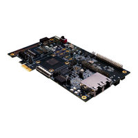
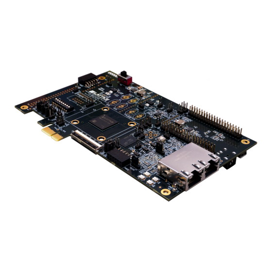
Lattice Semiconductor MachXO5T-NX-Development Board User Manual (71 pages)
Brand:
Lattice Semiconductor
| Category:
Motherboard
| Size: 3 MB
Table of Contents
Table of Contents
3
Acronyms in this Document
6
Introduction
7
Machxo5T-NX Development Board
7
Figure 1.1. Top View of Machxo5T-NX Development Board
7
Features
8
Figure 1.2. Bottom View of Machxo5T-NX Development Board
8
LFMXO5-100T Device
9
Applying Power to the Board
10
Figure 2.1. Board Power Supply
10
Table 2.1. Onboard Major Power Rails
11
Table 2.2. LFMXO5-100T IO Bank Power Rails Stuff
11
Table 2.3. LFMXO5-100T Major Power Rails Stuff
11
Hard JTAG/I C Programming
12
Figure 3.1. JTAG/I C Programming Architecture
12
Figure 3.2. Radiant Programmer Detect Dual Ports
12
JTAG Download Interface
13
Figure 3.3. Level Shift for JTAG Download Interface
13
Figure 3.4. JTAG Test Header
13
C Download Interface
14
Figure 3.5. I 2 C Programming Mode
14
Table 3.1. Config JTAG Connections
14
Table 3.2. Other Config JTAG Control Signals
14
Table 3.3. Download I C Connections
15
Soft JTAG/UART User Interface
16
Soft JTAG User Interface
16
Figure 4.1. JTAG/UART User Interfacing
16
Table 4.1. Soft JTAG Connections
16
Soft UART User Interface
17
Table 4.2. Soft UART Connections
17
LFMXO5-100T Clock Sources
18
Figure 5.1. Onboard Clock Resources
18
Table 5.1. Input Clock Options
18
SGMII Ethernet Connections
19
Figure 6.1. SGMII ×2 Interfacing
19
Table 6.1. SGMII Ethernet PHY Interfacing
19
Table 6.2. SGMII Ethernet PHY0 Strapping Configuration
20
Table 6.3. SGMII Ethernet PHY1 Strapping Configuration
20
Table 6.4. PHY Device VDD Power Supply Options
20
Pcie Gold Finger
21
Figure 7.1. Top Side of Pcie Edge Connector
21
Table 7.1. Gold Finger Pin Connections
21
Optional SMA Headers
22
Figure 8.1. SMA Interfacing for X1 Serdes RX and TX
22
Figure 8.2. SMA Interfacing for X1 Serdes Rx and Tx
22
Table 8.1. Connections for SMA Serdes Signal Pair
22
Table 8.2. Connections for External SMA Reference Clock
22
Figure 8.3. SMA Clock Input
23
Table 8.3. Single-End External SMA Clock
23
LPDDR4 Memory Controller Interface
24
Table 9.1. LPDDR4 Memory Controller Interconnections
24
Generating the Programming File
25
Figure 10.1. Radiant Software - Open Project Dialog Box
25
Figure 10.2. Radiant Software - Process Toolbar Initial State
25
Figure 10.3. Radiant Software - State of the Processes Toolbar Completion
26
Programming the Machxo5-NX Device
27
Figure 11.1. Radiant Software - Radiant Programmer
27
Figure 11.2. Radiant Programmer - Initial Opened
28
Figure 11.3. Radiant Programmer - Scan Device
28
Figure 11.4. Radiant Programmer - Device Detected
29
Figure 11.5. Radiant Programmer - Select Target Memory for Device Properties
29
Figure 11.6. Radiant Programmer - Device Properties for FLASH Configuration Memory
30
Figure 11.7. Radiant Programmer - Ready for Flash Programming
31
Figure 11.8. Radiant Programmer - Flash Programming Successful
31
Headers and Test Connections
32
Versa Headers
32
Table 12.1. Versa J8 Header Pin Connections
32
Table 12.2. Versa J9 Header Pin Connections
33
Arduino Board GPIO Headers
34
Table 12.3. Arduino J2 Pin Connections
34
Table 12.4. Arduino J3 Pin Connections
34
Table 12.5. Arduino J4 Pin Connections
34
FPC Headers
35
Table 12.6. Arduino J5 Pin Connections
35
Table 12.7. FPC Header Pin Connections
35
Aardvark Header (DNI)
36
Table 12.8. Aardvark J7 Header Pin Connections
36
Raspberry Pi Board GPIO Header
37
PMOD Headers
37
Table 12.9. Raspberry Pi J6 Header Pin Connections
37
Table 12.10. J15 Header Pin Connections
37
User I C Interface
38
ADC and Potentiometer
38
Table 12.11. J16 Header Pin Connections
38
Table 12.12. I C Connections
38
Figure 12.1. Circuit Design for ADC0
39
Figure 12.2. Circuit Design for ADC1
39
Figure 12.3. Trimmer Wiper Description
39
Leds and Switches
40
8-Position DIP Switch
40
Figure 13.1. Eight-Position DIP Switch Circuits
40
Figure 13.2. Eight-Position DIP Switch
40
Table 13.1. Four-Position DIP Switch Signals
40
General Purpose Push Buttons
41
General Purpose Leds
41
Table 13.2. Push Button Switch Signals
41
Table 13.3. LED Signals
41
Software Requirements
42
Storage and Handling
42
Ordering Information
42
Table 16.1 Ordering Information
42
Technical Support Assistance
43
Appendix A. Machxo5T-NX Development Board Schematics
44
Figure A. 1. Title Page
44
Figure A. 2. Block Diagram and Power Tree
45
Figure A. 3. USB to Hard JTAG I/F
46
Figure A. 4. USB to Soft JTAG I/F (BANK0)
47
Figure A. 5. Pmod0/Versa Connector (BANK1/2)
48
Figure A. 6. LPDDR4 (BANK3)
49
Figure A. 7. PCIE&FPC Headers (BANK4)
50
Figure A. 8. GBE and RJ45 (BANK5)
51
Figure A. 9. Multiple Headers (BANK6/7)
52
Figure A. 10. Power Rails
53
Figure A. 11. Power Regulators
54
Appendix B. Machxo5T-NX Development Board Bill of Materials
55
Appendix C. User Defined Preference File
63
Appendix D. Machxo5T-NX Development Board Errata
68
References
69
Revision History
70
Advertisement
Advertisement
Related Products
Lattice Semiconductor MachXO3
Lattice Semiconductor MachXO2 Series
Lattice Semiconductor MachXO3-940
Lattice Semiconductor MachXO
Lattice Semiconductor MachXO2280 Breakout Board
Lattice Semiconductor MachXO2-1200ZE
Lattice Semiconductor MachXO2 Breakout Board
Lattice Semiconductor MachX05-NX
Lattice Semiconductor MachXO3LF Starter Kit
Lattice Semiconductor MachXO5-NX Development Kit
Lattice Semiconductor Categories
Motherboard
Computer Hardware
Microcontrollers
Controller
Recording Equipment
More Lattice Semiconductor Manuals
Login
Sign In
OR
Sign in with Facebook
Sign in with Google
Upload manual
Upload from disk
Upload from URL