
Related Manuals for Holtek BS86DH12C


Summary of Contents for Holtek BS86DH12C
- Page 1 High Voltage Touch A/D Flash MCU with HVIO BS86DH12C Revision: V1.00 Date: October 26, 2018...
-
Page 2: Table Of Contents
BS86DH12C High Voltage Touch A/D Flash MCU with HVIO Table of Contents Features ......................... 7 CPU Features ..........................7 Peripheral Features ........................7 General Description ....................8 Block Diagram ....................... 9 Pin Assignment ..................... 9 Pin Descriptions ....................11 Absolute Maximum Ratings ................14 D.C. - Page 3 BS86DH12C High Voltage Touch A/D Flash MCU with HVIO Look-up Table ..........................28 Table Program Example ......................29 In Circuit Programming – ICP .....................30 On-Chip Debug Support – OCDS ....................31 Data Memory ....................... 31 Structure ............................31 Data Memory Addressing ......................32 General Purpose Data Memory ....................32 Special Purpose Data Memory ....................32...
- Page 4 BS86DH12C High Voltage Touch A/D Flash MCU with HVIO Input/Output Ports ....................63 Pull-high Resistors ........................63 Port A Wake-up ...........................64 I/O Port Control Registers ......................64 I/O Port Source Current Selection ....................64 I/O Port Sink Current Selection ....................66 Pin-shared Functions ........................68 I/O Pin Structures ........................72...
- Page 5 BS86DH12C High Voltage Touch A/D Flash MCU with HVIO Touch Key Interrupt ........................120 Programming Considerations ....................120 Over Current Protection – OCP ............... 121 Over Current Protection Operation ...................121 Over Current Protection Registers ....................122 Input Voltage Range ........................124 Input Offset Calibration ......................125 Over Voltage Protection –...
- Page 6 BS86DH12C High Voltage Touch A/D Flash MCU with HVIO Over Current Protection Interrupt ....................163 High Voltage Short Circuit Interrupt ...................163 TM Interrupts ..........................163 Interrupt Wake-up Function .......................163 Programming Considerations ....................164 Configuration Options ..................164 Application Circuits ..................165 Instruction Set ....................166 Introduction ..........................166...
-
Page 7: Features
BS86DH12C High Voltage Touch A/D Flash MCU with HVIO Features CPU Features • Operating voltage =8/12/16MHz, using internal LDO: V =5V (Typ.) ♦ High Voltage Driver: V =7V~10V ♦ • Up to 0.25μs instruction cycle with 16MHz system clock at V •... -
Page 8: General Description
BS86DH12C High Voltage Touch A/D Flash MCU with HVIO • Low voltage detect function • Package types: 20/28-pin SOP, 44-pin LQFP General Description The device is a Flash Memory type 8-bit high performance RISC architecture microcontroller with fully integrated touch key functions. With all touch key functions provided internally and with the convenience of Flash Memory multi-programming features, the device has all the features to offer designers a reliable and easy means of implementing touch keys within their products applications. -
Page 9: Block Diagram
BS86DH12C High Voltage Touch A/D Flash MCU with HVIO Block Diagram Port A PA0~PA7 Driver Timers Reset 8K × 16 512 × 8 Circuit Pin-Shared Port B PB0~PB7 Function Driver EEPROM Stack UART 64 × 8 8-Level Interrupt Port C... - Page 10 2. The OCDSDA and OCDSCK pins are supplied for the OCDS dedicated pins and as such only available for the BS86DHV12C device which is the OCDS EV chip for the BS86DH12C device. 3. For less pin-count package types there will be unbonded pins which should be properly configured to avoid unwanted current consumption resulting from floating input conditions.
-
Page 11: Pin Descriptions
BS86DH12C High Voltage Touch A/D Flash MCU with HVIO Pin Descriptions With the exception of the power pins, all pins on the device can be referenced by their Port name, e.g. PA0, PA1 etc., which refer to the digital I/O function of the pins. However these Port pins are also shared with other function such as the Touch Key function, Timer Module pins etc. - Page 12 BS86DH12C High Voltage Touch A/D Flash MCU with HVIO Description Pin Name Function PAPU General purpose I/O. Register enabled pull-up and PAWU CMOS wake-up PAS1 PA5/AN1/KEY6 PAS1 — A/D converter external input channel KEY6 PAS1 — Touch key input PAPU General purpose I/O.
- Page 13 BS86DH12C High Voltage Touch A/D Flash MCU with HVIO Description Pin Name Function PBPU CMOS General purpose I/O. Register enabled pull-up PBS1 PB4/CTP0/AN2/ CTP0 PBS1 — CMOS CTM0 output KEY7 PBS1 — A/D converter external input channel KEY7 PBS1 —...
-
Page 14: Absolute Maximum Ratings
BS86DH12C High Voltage Touch A/D Flash MCU with HVIO Description Pin Name Function — — Digital negative power supply, ground AVSS — — Analog negative power supply, ground VSS/AVSS/IOVSS/ HVSS IOVSS — — I/O port negative power supply, ground HVSS —... -
Page 15: D.c. Electrical Characteristics
BS86DH12C High Voltage Touch A/D Flash MCU with HVIO D.C. Electrical Characteristics For data in the following tables, note that factors such as oscillator type, operating voltage, operating frequency, pin load conditions, temperature and program instruction type, can all exert an influence on the measured values. -
Page 16: Standby Current Characteristics
BS86DH12C High Voltage Touch A/D Flash MCU with HVIO Standby Current Characteristics Ta=25°C, unless otherwise specified Test Conditions Max. Symbol Parameter Min. Typ. Max. Unit @85°C Conditions WDT on, LDO current SLEEP Mode — μA consumption included on, LDO current IDLE0 Mode –... -
Page 17: Internal Low Speed Oscillator Characteristics - Lirc
BS86DH12C High Voltage Touch A/D Flash MCU with HVIO 3. The minimum and maximum tolerance values provided in the table are only for the frequency at which the writer trims the HIRC oscillator. After trimming at this chosen specific frequency any change in HIRC oscillator frequency using the oscillator register control bits by the application program will give a frequency tolerance to within ±20%. -
Page 18: System Start Up Time Characteristics
BS86DH12C High Voltage Touch A/D Flash MCU with HVIO System Start Up Time Characteristics Ta=25°C Test Conditions Symbol Parameter Min. Typ. Max. Unit Conditions — /64, f — — HIRC HIRC System Start-up Time — — 1024 — Wake-up from Condition where f is Off —... -
Page 19: Input/Output Characteristics
BS86DH12C High Voltage Touch A/D Flash MCU with HVIO Input/Output Characteristics Ta=25°C Test Conditions Symbol Parameter Min. Typ. Max. Unit Conditions — Input Low Voltage for I/O Ports — — — 0.2V — Input High Voltage for I/O Ports —... -
Page 20: Lvd/Lvr Electrical Characteristics
BS86DH12C High Voltage Touch A/D Flash MCU with HVIO LVD/LVR Electrical Characteristics Ta=25°C Test Conditions Symbol Parameter Min. Typ. Max. Unit Conditions — LVR enable, voltage select 2.1V — LVR enable, voltage select 2.55V 2.55 Low Voltage Reset Voltage —... -
Page 21: Internal Reference Voltage Characteristics
BS86DH12C High Voltage Touch A/D Flash MCU with HVIO Internal Reference Voltage Characteristics Ta=25°C Test Conditions Symbol Parameter Min. Typ. Max. Unit Conditions Bandgap Reference Voltage — — 1.04 Turn-on Stable Time — No load — — μs Note: 1. All the above parameters are measured under conditions of no load condition unless otherwise described. -
Page 22: High Voltage I/O Other Electrical Characteristics
BS86DH12C High Voltage Touch A/D Flash MCU with HVIO Note: DET1 RLS1 DET2 RLS2 PWRRDY Undefined High Voltage I/O Other Electrical Characteristics Ta=25°C Test Conditions Symbol Parameter Min. Typ. Max. Unit Conditions Input Voltage — — — Accuracy — =10V 0.2V... - Page 23 BS86DH12C High Voltage Touch A/D Flash MCU with HVIO Test Conditions Symbol Parameter Min. Typ. Max. Unit Conditions Quiescent Current No load — μA ΔV Line Regulation — 6V≤V ≤10V, I =1mA — — LINE LOAD Temperature Coefficient — Ta=-40°C~85°C, I =10mA —...
-
Page 24: Ocp Electrical Characteristics
BS86DH12C High Voltage Touch A/D Flash MCU with HVIO OCP Electrical Characteristics Ta=25°C Test Conditions Symbol Parameter Min. Typ. Max. Unit Conditions OCPEN[1:0]=01B, Operating Current — 1250 μA DAC V =2.5V Without calibration — (OCPCOF[4:0]=10000B) Comparator Input Offset Voltage OS_CMP With calibration —... -
Page 25: Power-On Reset Characteristics
BS86DH12C High Voltage Touch A/D Flash MCU with HVIO Power-on Reset Characteristics Ta=25°C Test Conditions Symbol Parameter Min. Typ. Max. Unit Conditions Start Voltage to Ensure Power-on Reset — — — — Rising Rate to Ensure Power-on Reset — —... -
Page 26: Program Counter
BS86DH12C High Voltage Touch A/D Flash MCU with HVIO (System Clock) Phase Clock T1 Phase Clock T2 Phase Clock T3 Phase Clock T4 Program Counter PC+1 PC+2 Fetch Inst. (PC) Pipelining Execute Inst. (PC-1) Fetch Inst. (PC+1) Execute Inst. (PC) Fetch Inst. -
Page 27: Stack
BS86DH12C High Voltage Touch A/D Flash MCU with HVIO will be inserted. Manipulating the PCL register may cause program branching, so an extra cycle is needed to pre-fetch. Stack This is a special part of the memory which is used to save the contents of the Program Counter only. -
Page 28: Flash Program Memory
BS86DH12C High Voltage Touch A/D Flash MCU with HVIO • Branch decision: JMP, SZ, SZA, SNZ, SIZ, SDZ, SIZA, SDZA, CALL, RET, RETI, LSZ, LSZA, LSNZ, LSIZ, LSDZ, LSIZA, LSDZA Flash Program Memory The Program Memory is the location where the user code or program is stored. For this device the Program Memory is Flash type, which means it can be programmed and re-programmed a large number of times, allowing the user the convenience of code modification on the same device. - Page 29 BS86DH12C High Voltage Touch A/D Flash MCU with HVIO in the instruction. The higher order table data byte from the Program Memory will be transferred to the TBLH special register. The accompanying diagram illustrates the addressing data flow of the look-up table.
-
Page 30: In Circuit Programming - Icp
The provision of Flash type Program Memory provides the user with a means of convenient and easy upgrades and modifications to their programs on the same device. As an additional convenience, Holtek has provided a means of programming the microcontroller in-circuit using a 4-pin interface. This provides manufacturers with the possibility of manufacturing their circuit boards complete with a programmed or un-programmed microcontroller, and then programming or upgrading the program at a later stage. -
Page 31: On-Chip Debug Support - Ocds
There is an EV chip named BS86DHV12C which is used to emulate the real MCU device named BS86DH12C. The EV chip device also provides an “On-Chip Debug” function to debug the real MCU device during the development process. The EV chip and the real MCU device are almost functionally compatible except for “On-Chip Debug”... -
Page 32: Data Memory Addressing
BS86DH12C High Voltage Touch A/D Flash MCU with HVIO Special Purpose Data Memory (Sector 0 ~ Sector 1) General Purpose Data Memory (Sector 0 ~ Sector 3) Sector 0 Sector 1 Sector 3 Data Memory Structure Data Memory Addressing For this device that supports the extended instructions, there is no Bank Pointer for Data Memory addressing. - Page 33 BS86DH12C High Voltage Touch A/D Flash MCU with HVIO Sector 0 Sector 1 Sector 0 Sector 1 IAR0 PAS0 PDOM PAS1 PWRDET IAR1 PBS0 RSTC MP1L PBS1 MP1H PCS0 TKTMR TKC0 TK16DL TBLP TK16DH TBLH TKC1 TBHP TKM016DL STATUS TKM016DH...
-
Page 34: Special Function Register Description
BS86DH12C High Voltage Touch A/D Flash MCU with HVIO Special Function Register Description Most of the Special Function Register details will be described in the relevant functional sections. However, several registers require a separate description in this section. Indirect Addressing Registers – IAR0, IAR1, IAR2 The Indirect Addressing Registers, IAR0, IAR1 and IAR2, although having their locations in normal RAM register space, do not actually physically exist as normal registers. -
Page 35: Accumulator - Acc
BS86DH12C High Voltage Touch A/D Flash MCU with HVIO Indirect Addressing Program Example 2 data .section ´data´ adres1 db ? adres2 db ? adres3 db ? adres4 db ? block db ? code .section at 0 ´code´ org 00h start: mov a, 04h ;... -
Page 36: Program Counter Low Register - Pcl
BS86DH12C High Voltage Touch A/D Flash MCU with HVIO Program Counter Low Register – PCL To provide additional program control functions, the low byte of the Program Counter is made accessible to programmers by locating it within the Special Purpose area of the Data Memory. By manipulating this register, direct jumps to other program locations are easily implemented. - Page 37 BS86DH12C High Voltage Touch A/D Flash MCU with HVIO In addition, on entering an interrupt sequence or executing a subroutine call, the status register will not be pushed onto the stack automatically. If the contents of the status register are important and if the subroutine can corrupt the status register, precautions must be taken to correctly save it.
-
Page 38: Eeprom Data Memory
BS86DH12C High Voltage Touch A/D Flash MCU with HVIO EEPROM Data Memory The device contains an area of internal EEPROM Data Memory. EEPROM is by its nature a non- volatile form of re-programmable memory, with data retention even when its power supply is removed. -
Page 39: Reading Data From The Eeprom
BS86DH12C High Voltage Touch A/D Flash MCU with HVIO • EED Register Name Bit 7~0 D7~D0: Data EEPROM data bit 7 ~ bit 0 • EEC Register Name — — — — WREN RDEN — — — — — —... -
Page 40: Writing Data To The Eeprom
BS86DH12C High Voltage Touch A/D Flash MCU with HVIO the EED register. The data will remain in the EED register until another read or write operation is executed. The application program can poll the RD bit to determine when the data is valid for reading. - Page 41 BS86DH12C High Voltage Touch A/D Flash MCU with HVIO Programming Examples Reading data from the EEPROM – polling method MOV A, EEPROM_ADRES ; user defined address MOV EEA, A MOV A, 040H ; set memory pointer MP1L MOV MP1L, A ; MP1L points to EEC register MOV A, 01H ; set memory pointer MP1H MOV MP1H, A SET IAR1.1 ; set RDEN bit, enable read operations SET IAR1.0 ; start Read Cycle - set RD bit...
-
Page 42: Oscillators
BS86DH12C High Voltage Touch A/D Flash MCU with HVIO Oscillators Various oscillator types offer the user a wide range of functions according to their various application requirements. The flexible features of the oscillator functions ensure that the best optimisation can be achieved in terms of speed and power saving. -
Page 43: Internal High Speed Rc Oscillator - Hirc
BS86DH12C High Voltage Touch A/D Flash MCU with HVIO High Speed Oscillator HIRCEN HIRC IDLE0 Prescaler SLEEP Low Speed Oscillators CKS2~CKS0 IDLE2 LIRC SLEEP LIRC System Clock Configurations Internal High Speed RC Oscillator – HIRC The internal RC oscillator is a fully integrated system oscillator requiring no external components. - Page 44 BS86DH12C High Voltage Touch A/D Flash MCU with HVIO However, for some crystals, to ensure oscillation and accurate frequency generation, it is necessary to add two small value external capacitors, C1 and C2. The exact values of C1 and C2 should be selected in consultation with the crystal or resonator manufacturer’s specification.
-
Page 45: Operating Modes And System Clocks
As Holtek has provided the device with both high and low speed clock sources and the means to switch between them dynamically, the user can optimise the operation of their microcontroller to achieve the best performance/power ratio. -
Page 46: System Operation Modes
BS86DH12C High Voltage Touch A/D Flash MCU with HVIO System Operation Modes There are six different modes of operation for the microcontroller, each one with its own special characteristics and which can be chosen according to the specific performance and power requirements of the application. -
Page 47: Control Registers
BS86DH12C High Voltage Touch A/D Flash MCU with HVIO IDLE2 Mode The IDLE2 Mode is entered when an HALT instruction is executed and when the FHIDEN bit in the SCC register is high and the FSIDEN bit in the SCC register is low. In the IDLE2 Mode the CPU will be switched off but the high speed oscillator will be on to provide a clock source to keep some peripheral functions operational. - Page 48 BS86DH12C High Voltage Touch A/D Flash MCU with HVIO • HIRCC Register Name — — — — HIRC1 HIRC0 HIRCF HIRCEN — — — — — — — — Bit 7~4 Unimplemented, read as “0” HIRC1~HIRC0: HIRC frequency selection Bit 3~2...
-
Page 49: Operating Mode Switching
BS86DH12C High Voltage Touch A/D Flash MCU with HVIO Operating Mode Switching The device can switch between operating modes dynamically allowing the user to select the best performance/power ratio for the present task in hand. In this way microcontroller operations that do not require high performance can be executed using slower clocks thus requiring less operating current and prolonging battery life in portable applications. - Page 50 BS86DH12C High Voltage Touch A/D Flash MCU with HVIO FAST Mode to SLOW Mode Switching When running in the FAST Mode, which uses the high speed system oscillator, and therefore consumes more power, the system clock can switch to run in the SLOW Mode by set the CKS2~CKS0 bits to “111”...
- Page 51 BS86DH12C High Voltage Touch A/D Flash MCU with HVIO SLOW Mode to FAST Mode Switching In SLOW mode the system clock is derived from f . When system clock is switched back to the FAST mode from f , the CKS2~CKS0 bits should be set to “000”~“110” and then the system clock will respectively be switched to f /64.
- Page 52 BS86DH12C High Voltage Touch A/D Flash MCU with HVIO Entering the IDLE0 Mode There is only one way for the device to enter the IDLE0 Mode and that is to execute the “HALT” instruction in the application program with the FHIDEN bit in the SCC register equal to “0” and the FSIDEN bit in the SCC register equal to “1”.
-
Page 53: Standby Current Considerations
BS86DH12C High Voltage Touch A/D Flash MCU with HVIO Standby Current Considerations As the main reason for entering the SLEEP or IDLE Mode is to keep the current consumption of the device to as low a value as possible, perhaps only in the order of several micro-amps except in the IDLE1 and IDLE2 Mode, there are other considerations which must also be taken into account by the circuit designer if the power consumption is to be minimised. -
Page 54: Watchdog Timer
BS86DH12C High Voltage Touch A/D Flash MCU with HVIO Watchdog Timer The Watchdog Timer is provided to prevent program malfunctions or sequences from jumping to unknown locations, due to certain uncontrollable external events such as electrical noise. Watchdog Timer Clock Source... -
Page 55: Watchdog Timer Operation
BS86DH12C High Voltage Touch A/D Flash MCU with HVIO LRF: LVRC register software reset flag Bit 1 Described elsewhere Bit 0 WRF: WDTC register software reset flag 0: Not occurred 1: Occurred This bit is set high by the WDTC register software reset and cleared to zero by the application program. -
Page 56: Reset And Initialisation
BS86DH12C High Voltage Touch A/D Flash MCU with HVIO Reset and Initialisation A reset function is a fundamental part of any microcontroller ensuring that the device can be set to some predetermined condition irrespective of outside parameters. The most important reset condition is after power is first applied to the microcontroller. - Page 57 BS86DH12C High Voltage Touch A/D Flash MCU with HVIO • RSTC Register Name RSTC7 RSTC6 RSTC5 RSTC4 RSTC3 RSTC2 RSTC1 RSTC0 Bit 7~0 RSTC7~RSTC0: Reset function control 01010101: No operation 10101010: No operation Other values: Reset MCU If these bits are changed due to adverse environmental conditions, the microcontroller will be reset.
- Page 58 BS86DH12C High Voltage Touch A/D Flash MCU with HVIO RSTD Internal Reset Low Voltage Reset Timing Chart • LVRC Register Name LVS7 LVS6 LVS5 LVS4 LVS3 LVS2 LVS1 LVS0 Bit 7~0 LVS7~LVS0: LVR voltage selection 01010101: 2.1V 00110011: 2.55V 10011001: 3.15V 10101010: 3.8V...
-
Page 59: Reset Initial Conditions
BS86DH12C High Voltage Touch A/D Flash MCU with HVIO Watchdog Time-out Reset during Normal Operation The Watchdog time-out flag TO will be set to “1” when Watchdog time-out Reset during normal operation. WDT Time-out RSTD Internal Reset WDT Time-out Reset during Normal Operation Timing Chart... - Page 60 BS86DH12C High Voltage Touch A/D Flash MCU with HVIO The different kinds of resets all affect the internal registers of the microcontroller in different ways. To ensure reliable continuation of normal program execution after a reset occurs, it is important to know what condition the microcontroller is in after a particular reset occurs.
- Page 61 BS86DH12C High Voltage Touch A/D Flash MCU with HVIO LVR Reset WDT Time-out WDT Time-out Register Power On Reset (Normal Operation) (Normal Operation) (IDLE/SLEEP) TXR_RXR x x x x x x x x x x x x x x x x...
- Page 62 BS86DH12C High Voltage Touch A/D Flash MCU with HVIO LVR Reset WDT Time-out WDT Time-out Register Power On Reset (Normal Operation) (Normal Operation) (IDLE/SLEEP) TKM2ROL 0 0 0 0 0 0 0 0 0 0 0 0 0 0 0 0...
-
Page 63: Input/Output Ports
High Voltage Touch A/D Flash MCU with HVIO Input/Output Ports Holtek microcontrollers offer considerable flexibility on their I/O ports. With the input or output designation of every pin fully under user program control, pull-high selections for all ports and wake-up selections on certain pins, the user is provided with an I/O structure to meet the needs of a wide range of application possibilities. -
Page 64: Port A Wake-Up
BS86DH12C High Voltage Touch A/D Flash MCU with HVIO Port A Wake-up The HALT instruction forces the microcontroller into the SLEEP or IDLE Mode which preserves power, a feature that is important for battery and other low-power applications. Various methods exist to wake-up the microcontroller, one of which is to change the logic condition on one of the Port A pins from high to low. - Page 65 BS86DH12C High Voltage Touch A/D Flash MCU with HVIO Register Name SLEDC0 SLEDC07 SLEDC06 SLEDC05 SLEDC04 SLEDC03 SLEDC02 SLEDC01 SLEDC00 SLEDC1 — — — — SLEDC13 SLEDC12 SLEDC11 SLEDC10 I/O Port Source Current Selection Register List • SLEDC0 Register Name...
-
Page 66: I/O Port Sink Current Selection
BS86DH12C High Voltage Touch A/D Flash MCU with HVIO I/O Port Sink Current Selection The device supports different output sink current driving capability for each I/O port. With the selection register, SLEDCOMn, specific I/O port can support two levels of the sink current driving capability. - Page 67 BS86DH12C High Voltage Touch A/D Flash MCU with HVIO • SLEDCOM1 Register Name PBNS7 PBNS6 PBNS5 PBNS4 PBNS3 PBNS2 PBNS1 PBNS0 Bit 7 PBNS7: PB7 sink current selection 0: Sink current=Level 0 (Min.) 1: Sink current=Level 1 (Max.) Bit 6 PBNS6: PB6 sink current selection 0: Sink current=Level 0 (Min.)
-
Page 68: Pin-Shared Functions
BS86DH12C High Voltage Touch A/D Flash MCU with HVIO PCNS0: PC0 sink current selection Bit 0 0: Sink current=Level 0 (Min.) 1: Sink current=Level 1 (Max.) Pin-shared Functions The flexibility of the microcontroller range is greatly enhanced by the use of pins that have more than one function. - Page 69 BS86DH12C High Voltage Touch A/D Flash MCU with HVIO • PAS0 Register Name PAS07 PAS06 PAS05 PAS04 PAS03 PAS02 PAS01 PAS00 Bit 7~6 PAS07~PAS06: PA3 pin-shared function selection 00: PA3/PTPI 01: SDA 10: VREF 11: KEY4 Bit 5~4 PAS05~PAS04: PA2 pin-shared function selection...
- Page 70 BS86DH12C High Voltage Touch A/D Flash MCU with HVIO • PBS0 Register Name PBS07 PBS06 PBS05 PBS04 PBS03 PBS02 PBS01 PBS00 Bit 7~6 PBS07~PBS06: PB3 pin-shared function selection 00: PB3 01: SDA 10: AN7 11: KEY10 Bit 5~4 PBS05~PBS04: PB2 pin-shared function selection...
- Page 71 BS86DH12C High Voltage Touch A/D Flash MCU with HVIO • PCS0 Register Name PCS07 PCS06 PCS05 PCS04 PCS03 PCS02 PCS01 PCS00 Bit 7~6 PCS07~PCS06: PC3 pin-shared function selection 00: PC3 01: CTP0 10: SDA 11: TX Bit 5~4 PCS05~PCS04: PC2 pin-shared function selection...
-
Page 72: I/O Pin Structures
BS86DH12C High Voltage Touch A/D Flash MCU with HVIO • IFS1 Register Name — — — — PTPIPS PTCKPS CTCK1PS CTCK0PS — — — — — — — — Bit 7~4 Unimplemented, read as “0” PTPIPS: PTPI input source pin selection... -
Page 73: High Voltage I/O Port
BS86DH12C High Voltage Touch A/D Flash MCU with HVIO data registers are first programmed. Selecting which pins are inputs and which are outputs can be achieved byte-wide by loading the correct values into the appropriate port control register or by programming individual bits in the port control register using the “SET [m].i”... -
Page 74: High Voltage I/O Registers
BS86DH12C High Voltage Touch A/D Flash MCU with HVIO PDn_OE: PDn output global enable signal PDn_DIN: PDn input data 3. When the comparison result between PDn_DOUT and PDn_DIN is different, the LIRC oscillator will be enabled by the hardware until the short circuit condition is released even if the CPU and LIRC are both off. -
Page 75: Voltage Detector
BS86DH12C High Voltage Touch A/D Flash MCU with HVIO • PDC Register Name — — PDC5 PDC4 PDC3 PDC2 PDC1 PDC0 — — — — Bit 7~6 Unimplemented, read as “0” PDC5~PDC0: HVIO PD5~PD0 pin input/output type selection Bit 5~0... -
Page 76: Short-Circuit Protection Function
BS86DH12C High Voltage Touch A/D Flash MCU with HVIO Voltage Detector PWRRDY Reference VCC2 Voltage Detector Level VCC2 PWRRDYF Shift VCC1 VCC1 VCC2 Level Level CWSEL1 CWSEL2 Shift Shift R11=12kΩ R21=12kΩ CC1O CC2O (To A/D Converter) (To A/D Converter) R12=3kΩ... -
Page 77: Low Dropout Regulator - Ldo
BS86DH12C High Voltage Touch A/D Flash MCU with HVIO Low Dropout Regulator – LDO The device includes an internal low dropout regulator, LDO. The LDO can reduce the higher input voltage on the VCC1 pin, which ranges from 6V to 10V, to a stable 5V voltage and then output on the VLDO pin. -
Page 78: Tm Clock Source
BS86DH12C High Voltage Touch A/D Flash MCU with HVIO comparators. When the free running count-up counter has the same value as the pre-programmed comparator, known as a compare match situation, a TM interrupt signal will be generated which can clear the counter and perhaps also change the condition of the TM output pin. The internal TM counter is driven by a user selectable clock source, which can be an internal clock or an external pin. -
Page 79: Programming Considerations
BS86DH12C High Voltage Touch A/D Flash MCU with HVIO Clock input CTCKn CTMn CCR output CTPn CTPnB CTM Function Pin Block Diagram (n=0~1) Clock/capture input PTCK CCR capture input PTPI CCR output PTPB PTM Function Pin Block Diagram Programming Considerations The TM Counter Registers and the Capture/Compare CCRA and CCRP registers, all have a low and high byte structure. -
Page 80: Compact Type Tm - Ctm
BS86DH12C High Voltage Touch A/D Flash MCU with HVIO Step 2. Write data to High Byte xTMnAH or PTMRPH ♦ – Here data is written directly to the high byte registers and simultaneously data is latched from the 8-bit buffer to the Low Byte registers. -
Page 81: Compact Type Tm Register Description
BS86DH12C High Voltage Touch A/D Flash MCU with HVIO Compact Type TM Register Description Overall operation of the Compact TM is controlled using a series of registers. A read only register pair exists to store the internal counter 10-bit value, while a read/write register pair exists to store the internal 10-bit CCRA value. - Page 82 BS86DH12C High Voltage Touch A/D Flash MCU with HVIO If the CTMn is in the Compare Match Output Mode or the PWM Output Mode, then the CTMn output pin will be reset to its initial condition, as specified by the CTnOC bit, when the CTnON bit changes from low to high.
- Page 83 BS86DH12C High Voltage Touch A/D Flash MCU with HVIO when a compare match occurs. After the CTMn output pin changes state, it can be reset to its initial level by changing the level of the CTnON bit from low to high.
-
Page 84: Compact Type Tm Operation Modes
BS86DH12C High Voltage Touch A/D Flash MCU with HVIO • CTMnDH Register Name — — — — — — — — — — — — — — — — — — Bit 7~2 Unimplemented, read as “0” D9~D8: CTMn Counter High Byte Register bit 1 ~ bit 0... - Page 85 BS86DH12C High Voltage Touch A/D Flash MCU with HVIO request flag, generated from a compare match occurs from Comparator P, will have no effect on the CTMn output pin. The way in which the CTMn output pin changes state are determined by the condition of the CTnIO1 and CTnIO0 bits in the CTMnC1 register.
- Page 86 BS86DH12C High Voltage Touch A/D Flash MCU with HVIO Counter Value CTnCCLR = 1; CTnM [1:0] = 00 CCRA = 0 CCRA > 0 Counter cleared by CCRA value Counter overflow 0x3FF CCRA=0 Resume CCRA Pause Stop Counter Restart CCRP...
- Page 87 BS86DH12C High Voltage Touch A/D Flash MCU with HVIO Timer/Counter Mode To select this mode, bits CTnM1 and CTnM0 in the CTMnC1 register should be set to “11” respectively. The Timer/Counter Mode operates in an identical way to the Compare Match Output Mode generating the same interrupt flags.
- Page 88 BS86DH12C High Voltage Touch A/D Flash MCU with HVIO Counter Value CTnDPX = 0; CTnM [1:0] = 10 Counter cleared by CCRP Counter Reset when CTnON returns high CCRP Counter Stop if Pause Resume CTnON bit low CCRA Time CTnON...
- Page 89 BS86DH12C High Voltage Touch A/D Flash MCU with HVIO Counter Value CTnDPX = 1; CTnM [1:0] = 10 Counter cleared by CCRA Counter Reset when CTnON returns high CCRA Counter Stop if Pause Resume CTnON bit low CCRP Time CTnON...
-
Page 90: Periodic Type Tm - Ptm
BS86DH12C High Voltage Touch A/D Flash MCU with HVIO Periodic Type TM – PTM The Periodic Type TM contains five operating modes, which are Compare Match Output, Timer/ Event Counter, Capture Input, Single Pulse Output and PWM Output modes. The Periodic TM can also be controlled with two external input pins and can drive two external output pins. - Page 91 BS86DH12C High Voltage Touch A/D Flash MCU with HVIO Register Name PTMC0 PTPAU PTCK2 PTCK1 PTCK0 PTON — — — PTMC1 PTM1 PTM0 PTIO1 PTIO0 PTOC PTPOL PTCAPTS PTCCLR PTMDL PTMDH — — — — — — PTMAL PTMAH —...
- Page 92 BS86DH12C High Voltage Touch A/D Flash MCU with HVIO • PTMC1 Register Name PTM1 PTM0 PTIO1 PTIO0 PTOC PTPOL PTCAPTS PTCCLR Bit 7~6 PTM1~PTM0: Select PTM Operating Mode 00: Compare Match Output Mode 01: Capture Input Mode 10: PWM Output Mode or Single Pulse Output Mode 11: Timer/Counter Mode These bits set the required operating mode for the PTM.
- Page 93 BS86DH12C High Voltage Touch A/D Flash MCU with HVIO PTOC: PTM PTP output control Bit 3 Compare Match Output Mode 0: Initial low 1: Initial high PWM Output Mode/Single Pulse Output Mode 0: Active low 1: Active high This is the output control bit for the PTM output pin. Its operation depends upon whether PTM is being used in the Compare Match Output Mode or in the PWM Output Mode/Single Pulse Output Mode.
- Page 94 BS86DH12C High Voltage Touch A/D Flash MCU with HVIO • PTMAL Register Name Bit 7~0 D7~D0: PTM CCRA Low Byte Register bit 7 ~ bit 0 PTM 10-bit CCRA bit 7 ~ bit 0 • PTMAH Register Name — —...
-
Page 95: Periodic Type Tm Operation Modes
BS86DH12C High Voltage Touch A/D Flash MCU with HVIO Periodic Type TM Operation Modes The Periodic Type TM can operate in one of five operating modes, Compare Match Output Mode, PWM Output Mode, Single Pulse Output Mode, Capture Input Mode or Timer/Counter Mode. The operating mode is selected using the PTM1 and PTM0 bits in the PTMC1 register. - Page 96 BS86DH12C High Voltage Touch A/D Flash MCU with HVIO Counter overflow Counter Value PTCCLR = 0; PTM [1:0] = 00 CCRP > 0 CCRP=0 Counter cleared by CCRP value 0x3FF CCRP > 0 Counter Resume Restart CCRP Pause Stop CCRA...
- Page 97 BS86DH12C High Voltage Touch A/D Flash MCU with HVIO Counter Value PTCCLR = 1; PTM [1:0] = 00 CCRA = 0 CCRA > 0 Counter cleared by CCRA value Counter overflow 0x3FF CCRA=0 Resume CCRA Pause Stop Counter Restart CCRP...
- Page 98 BS86DH12C High Voltage Touch A/D Flash MCU with HVIO Timer/Counter Mode To select this mode, bits PTM1 and PTM0 in the PTMC1 register should be set to “11” respectively. The Timer/Counter Mode operates in an identical way to the Compare Match Output Mode generating the same interrupt flags.
- Page 99 BS86DH12C High Voltage Touch A/D Flash MCU with HVIO Counter Value PTM [1:0] = 10 Counter cleared by CCRP Counter Reset when PTON returns high CCRP Counter Stop if Pause Resume PTON bit low CCRA Time PTON PTPAU PTPOL CCRA Int.
- Page 100 BS86DH12C High Voltage Touch A/D Flash MCU with HVIO Single Pulse Output Mode To select this mode, bits PTM1 and PTM0 in the PTMC1 register should be set to “10” respectively and also the PTIO1 and PTIO0 bits should be set to “11” respectively. The Single Pulse Output Mode, as the name suggests, will generate a single shot pulse on the PTM output pin.
- Page 101 BS86DH12C High Voltage Touch A/D Flash MCU with HVIO Counter Value PTM [1:0] = 10; PTIO [1:0] = 11 Counter stopped by CCRA Counter Reset when PTON returns high CCRA Counter Stops by Resume Pause software CCRP Time PTON Auto. set by...
- Page 102 BS86DH12C High Voltage Touch A/D Flash MCU with HVIO Capture Input Mode To select this mode bits PTM1 and PTM0 in the PTMC1 register should be set to “01” respectively. This mode enables external signals to capture and store the present value of the internal counter and can therefore be used for applications such as pulse width measurements.
- Page 103 BS86DH12C High Voltage Touch A/D Flash MCU with HVIO Counter Value PTM [1:0] = 01 Counter cleared by CCRP Counter Counter Stop Reset CCRP Resume Pause Time PTON PTPAU Active Active Active edge edge edge PTM Capture pin PTPI or PTCK CCRA Int.
-
Page 104: Analog To Digital Converter
BS86DH12C High Voltage Touch A/D Flash MCU with HVIO Analog to Digital Converter The need to interface to real world analog signals is a common requirement for many electronic systems. However, to properly process these signals by a microcontroller, they must first be converted into digital signals by A/D converters. -
Page 105: A/D Converter Register Description
BS86DH12C High Voltage Touch A/D Flash MCU with HVIO A/D Converter Register Description Overall operation of the A/D converter is controlled using five registers. A read only register pair exists to store the A/D Converter data 12-bit value. The remaining two registers, SADC0 and SADC1, are control registers which set the operating conditions and control function of the A/D converter. - Page 106 BS86DH12C High Voltage Touch A/D Flash MCU with HVIO • SADC0 Register Name START ADBZ ADCEN ADRFS SACS3 SACS2 SACS1 SACS0 Bit 7 START: Start the A/D conversion 0→1→0: Start This bit is used to initiate an A/D conversion process. The bit is normally low but if set high and then cleared low again, the A/D converter will initiate a conversion process.
-
Page 107: A/D Converter Reference Voltage
BS86DH12C High Voltage Touch A/D Flash MCU with HVIO • SADC1 Register Name SAINS2 SAINS1 SAINS0 SAVRS1 SAVRS0 SACKS2 SACKS1 SACKS0 Bit 7~5 SAINS2~SAINS0: A/D converter input signal selection 000: External source – External analog channel intput, ANn 001: Internal source – Internal bandgap reference voltage, V 010: Internal source –... -
Page 108: A/D Converter Input Signals
BS86DH12C High Voltage Touch A/D Flash MCU with HVIO A/D Converter Input Signals All of the external A/D analog input pins are pin-shared with the I/O pins as well as other functions. The corresponding pin-shared function control bits in the PxS0 and PxS1 registers determine whether the external input pins are set as A/D converter analog channel inputs or whether they have other functions. -
Page 109: Conversion Rate And Timing Diagram
BS86DH12C High Voltage Touch A/D Flash MCU with HVIO that can be selected. As the recommended range of permissible A/D clock period, t , is from 0.5μs ADCK to 10μs, care must be taken for system clock frequencies. For example, if the system clock operates at a frequency of 8MHz, the SACKS2~SACKS0 bits should not be set to 000, 001 or 111. -
Page 110: Summary Of A/D Conversion Steps
BS86DH12C High Voltage Touch A/D Flash MCU with HVIO ON2ST ADCEN A/D sampling time A/D sampling time START Start of A/D conversion Start of A/D conversion Start of A/D conversion ADBZ End of A/D End of A/D conversion conversion SACS[3:0]... -
Page 111: Programming Considerations
BS86DH12C High Voltage Touch A/D Flash MCU with HVIO • Step 9 The A/D conversion procedure can now be initialized by setting the START bit from low to high and then low again. • Step 10 If A/D conversion is in progress, the ADBZ flag will be set high. After the A/D conversion process is complete, the ADBZ flag will go low and then the output data can be read from SADOH and SADOL registers. -
Page 112: A/D Programming Examples
BS86DH12C High Voltage Touch A/D Flash MCU with HVIO A/D Programming Examples The following two programming examples illustrate how to set and implement an A/D conversion. In the first example, the method of polling the ADBZ bit in the SADC0 register is used to detect when the conversion cycle is complete, whereas in the second example, the A/D interrupt is used to determine when the conversion is complete. - Page 113 BS86DH12C High Voltage Touch A/D Flash MCU with HVIO Example: using the interrupt method to detect the end of conversion clr ADE ; disable ADC interrupt mov a,03H ; select f /8 as A/D clock mov SADC1,a ; A/D input signal comes from external channel ; select VREF pin as A/D reference voltage source mov a,80h mov PAS0,a ; set PAS0 to configure pin VREF...
-
Page 114: Touch Key Function
BS86DH12C High Voltage Touch A/D Flash MCU with HVIO Touch Key Function The device provides multiple touch key functions. The touch key function is fully integrated and requires no external components, allowing touch key functions to be implemented by the simple manipulation of internal registers. - Page 115 BS86DH12C High Voltage Touch A/D Flash MCU with HVIO Register Name TKTMR TKC0 — TKRCOV TKST TKCFOV TK16OV TSCS TK16S1 TK16S0 TKC1 — — — — — — TKFS1 TKFS0 TK16DL TK16DH TKMn16DL TKMn16DH TKMnROL TKMnROH — — — —...
- Page 116 BS86DH12C High Voltage Touch A/D Flash MCU with HVIO TKST: Touch key detection Start control Bit 5 0: Stopped or no operation 0→1: Start detection In all modules the touch key module 16-bit C/F counter, touch key function 16-bit counter and 5-bit time slot unit period counter will automatically be cleared when this bit is cleared to zero.
- Page 117 BS86DH12C High Voltage Touch A/D Flash MCU with HVIO • TKMn16DH/TKMn16DL – Touch Key Module n 16-bit C/F Counter Register Pair Register TKMn16DH TKMn16DL Name D15 D14 D13 D12 D11 D10 D9 This register pair is used to store the touch key module n 16-bit C/F counter value. This 16-bit C/F counter will be stopped and the counter content will be kept unchanged when the touch key time slot counter overflows.
- Page 118 BS86DH12C High Voltage Touch A/D Flash MCU with HVIO MnSOF2~MnSOF0: Touch key module n Reference and Key oscillators hopping Bit 2~0 frequency selection (MnSOFC=0) 000: 1.020MHz 001: 1.040MHz 010: 1.059MHz 011: 1.074MHz 100: 1.085MHz 101: 1.099MHz 110: 1.111MHz 111: 1.125MHz These bits are used to select the touch key oscillator frequency for the hopping function.
- Page 119 BS86DH12C High Voltage Touch A/D Flash MCU with HVIO MnK1EN: Touch key module n Key 1 enable control Bit 0 Touch Key Module n – Mn MnK1EN 0: Disable I/O or other functions 1: Enable KEY1 KEY5 KEY9 Touch Key Operation When a finger touches or is in proximity to a touch pad, the capacitance of the pad will increase.
-
Page 120: Touch Key Interrupt
BS86DH12C High Voltage Touch A/D Flash MCU with HVIO timer counter will be automatically switched off when the time slot counter overflows. The clock source for the time slot counter is sourced from the reference oscillator or f /4 which is selected using the MnTSS bit in the TKMnC1 register. -
Page 121: Over Current Protection - Ocp
BS86DH12C High Voltage Touch A/D Flash MCU with HVIO Over Current Protection – OCP The device includes an over current protection function which provides a protection mechanism for applications. The current on the OCPI pin is converted to a relevant voltage level according to the current value using the OCP operational amplifier. -
Page 122: Over Current Protection Registers
BS86DH12C High Voltage Touch A/D Flash MCU with HVIO Over Current Protection Registers Overall operation of the over current protection is controlled using several registers. The OCPDA register is used to provide the reference voltage for the over current protection circuit. The OCPOCAL and OCPCCAL registers are used to cancel out the operational amplifier and comparator input offset. - Page 123 BS86DH12C High Voltage Touch A/D Flash MCU with HVIO • OCPC1 Register Name — — OCPDEB2 OCPDEB1 OCPDEB0 — — — — Bit 7~6 Unimplemented, read as “0” G2~G0: PGA R2/R1 ratio selection Bit 5~3 000: Unity gain buffer (non-inverting mode) or R2/R1=1 (inverting mode)
-
Page 124: Input Voltage Range
BS86DH12C High Voltage Touch A/D Flash MCU with HVIO OCPORSP: OCP Operational Amplifier Input Offset Voltage Calibration Reference Bit 6 selection 0: Select negative input as the reference input 1: Select positive input as the reference input Bit 5~0 OCPOOF5~OCPOOF0: OCP Operational Amplifier Input Offset Voltage Calibration... -
Page 125: Input Offset Calibration
BS86DH12C High Voltage Touch A/D Flash MCU with HVIO • For input voltages 0 > V > -0.2V, the PGA operates in the inverting mode and the PGA output is obtained using the formula below. Note that if the input voltage is negative, it cannot be lower than -0.2V which will result in current leakage. -
Page 126: Over Voltage Protection - Ovp
BS86DH12C High Voltage Touch A/D Flash MCU with HVIO Step6. Restore the comparator input offset calibration value V into the OCPCOF[4:0] bit field. The offset Calibration procedure is now finished. Where V COS1 COS2 Note: S4 is on and the D/A converter is off. This situation is only available for comparator calibration procedure. -
Page 127: Over Voltage Protection Registers
BS86DH12C High Voltage Touch A/D Flash MCU with HVIO Over Voltage Protection Registers Overall operation of the OVP function is controlled using several registers. The OVPDA register is used to provide the reference voltage for the OVP circuit. The OVPC0~OVPC2 control registers are used to control the OVP function, D/A converter reference voltage selection, comparator de-bounce time selection, comparator hysteresis function and comparator output polarity control, etc. -
Page 128: Comparator Input Offset Cancellation
BS86DH12C High Voltage Touch A/D Flash MCU with HVIO • OVPC1 Register Name OVPCOUT OVPCOFM OVPCRS OVPCOF4 OVPCOF3 OVPCOF2 OVPCOF1 OVPCOF0 Bit 7 OVPCOUT: OVP comparator output bit 0: Positive input voltage < negative input voltage 1: Positive input voltage > negative input voltage... -
Page 129: I 2 C Interface
BS86DH12C High Voltage Touch A/D Flash MCU with HVIO Step1: Set OVPCOFM=1, OVPCRS=1, the OVP is now in the comparator offset calibration mode, S0 and S2 are on. To make sure V as minimised as possible after calibration, the input reference voltage in calibration mode should be the same as input DC operating voltage in normal mode operation. - Page 130 BS86DH12C High Voltage Touch A/D Flash MCU with HVIO still applicable even if the I C device is activated and the related internal pull-high function could be controlled by its corresponding pull-high control register. Data Bus C Data Register C Address Register...
-
Page 131: I 2 C Registers
BS86DH12C High Voltage Touch A/D Flash MCU with HVIO C Debounce Time Selection I C Standard Mode (100kHz) I C Fast Mode (400kHz) No Debounce > 2MHz > 5MHz 2 system clock debounce > 4MHz > 10MHz 4 system clock debounce >... - Page 132 BS86DH12C High Voltage Touch A/D Flash MCU with HVIO C Control Registers There are three control registers for the I C interface, IICC0, IICC1 and IICTOC. The IICC0 register is used to control the enable/disable function and to set the data transmission clock frequency.
-
Page 133: I 2 C Bus Communication
BS86DH12C High Voltage Touch A/D Flash MCU with HVIO HBB: I Bit 5 C Bus busy flag 0: I C Bus is not busy 1: I C Bus is busy The HBB flag is the I C busy flag. This flag will be “1” when the I C bus is busy which will occur when a START signal is detected. - Page 134 BS86DH12C High Voltage Touch A/D Flash MCU with HVIO data transfer completion or from the I C bus time-out occurrence. During a data transfer, note that after the 7-bit slave address has been transmitted, the following bit, which is the 8th bit, is the read/ write bit whose value will be placed in the SRW bit.
- Page 135 BS86DH12C High Voltage Touch A/D Flash MCU with HVIO As an I C bus interrupt can come from three sources, when the program enters the interrupt subroutine, the HAAS and IICTOF bits should be examined to see whether the interrupt source has come from a matching slave address or from the completion of a data byte transfer or from the C bus time-out occurrence.
- Page 136 BS86DH12C High Voltage Touch A/D Flash MCU with HVIO Start Slave Address Data Stop S=Start (1 bit) SA=Slave Address (7 bits) SR=SRW bit (1 bit) M=Slave device send acknowledge bit (1 bit) D=Data (8 bits) A=ACK (RXAK bit for transmitter, TXAK bit for receiver, 1 bit)
-
Page 137: I 2 C Time-Out Control
BS86DH12C High Voltage Touch A/D Flash MCU with HVIO C Time-out Control In order to reduce the problem of I C lockup due to reception of erroneous clock sources, a time-out function is provided. If the clock source to the I... -
Page 138: Uart Interface
BS86DH12C High Voltage Touch A/D Flash MCU with HVIO IICTOF: I Bit 6 C Time-out flag 0: No time-out occurred 1: Time-out occurred IICTOS5~IICTOS0: I Bit 5~0 C Time-out period selection C time-out clock source is f /32. C time-out time is equal to (IICTOS[5:0]+1)×(32/f... -
Page 139: Uart External Pins
BS86DH12C High Voltage Touch A/D Flash MCU with HVIO UART External Pins To communicate with an external serial interface, the internal UART has two external pins known as TX and RX. The TX and RX pins are the UART transmitter and receiver pins respectively. The TX and RX pin function should first be selected by the corresponding pin-shared function selection register before the UART function is used. - Page 140 BS86DH12C High Voltage Touch A/D Flash MCU with HVIO • USR Register The USR register is the status register for the UART, which can be read by the program to determine the present status of the UART. All flags within the USR register are read only. Further explanation...
- Page 141 BS86DH12C High Voltage Touch A/D Flash MCU with HVIO RXIF: Receive TXR_RXR data register status Bit 2 0: TXR_RXR data register is empty 1: TXR_RXR data register has available data The RXIF flag is the receive data register status flag. When this read only flag is “0”, it indicates that the TXR_RXR read data register is empty.
- Page 142 BS86DH12C High Voltage Touch A/D Flash MCU with HVIO TIDLE, TXIF and RIDLE bits will be set. Other control bits in UCR1, UCR2 and BRG registers will remain unaffected. If the UART is active and the UARTEN bit is cleared, all pending transmissions and receptions will be terminated and the module will be reset as defined above.
- Page 143 BS86DH12C High Voltage Touch A/D Flash MCU with HVIO • UCR2 Register The UCR2 register is the second of the two UART control registers and serves several purposes. One of its main functions is to control the basic enable/disable operation of the UART Transmitter and Receiver as well as enabling the various UART interrupt sources.
- Page 144 BS86DH12C High Voltage Touch A/D Flash MCU with HVIO off. There will be no RX pin wake-up UART function if the UART clock (f ) exists. If the WAKE bit is set to 1 as the UART clock (f ) is switched off, a UART wake-up request will be initiated when a falling edge on the RX pin occurs.
-
Page 145: Baud Rate Generator
BS86DH12C High Voltage Touch A/D Flash MCU with HVIO Baud Rate Generator To set the speed of the serial data communication, the UART function contains its own dedicated baud rate generator. The baud rate is controlled by its own internal free running 8-bit timer, the period of which is determined by two factors. -
Page 146: Uart Transmitter
BS86DH12C High Voltage Touch A/D Flash MCU with HVIO and status flags with bits TXEN, RXEN, TXBRK, RXIF, OERR, FERR, PERR and NF being cleared while bits TIDLE, TXIF and RIDLE will be set. The remaining control bits in the UCR1, UCR2 and BRG registers will remain unaffected. - Page 147 BS86DH12C High Voltage Touch A/D Flash MCU with HVIO TXEN bit is set, but the data will not be transmitted until the TXR_RXR register has been loaded with data and the baud rate generator has defined a shift clock source. However, the transmission can also be initiated by first loading data into the TXR_RXR register, after which the TXEN bit can be set.
-
Page 148: Uart Receiver
BS86DH12C High Voltage Touch A/D Flash MCU with HVIO last break character and subsequently send out one or two stop bits. The automatic logic highs at the end of the last break character will ensure that the start bit of the next frame is recognized. -
Page 149: Managing Receiver Errors
BS86DH12C High Voltage Touch A/D Flash MCU with HVIO a start bit, data bits and the invalid stop bit and the FERR flag will be set. The receiver must wait for a valid stop bit before looking for the next start bit. The receiver will not make the assumption that the break condition on the line is the next start bit. -
Page 150: Uart Interrupt Structure
BS86DH12C High Voltage Touch A/D Flash MCU with HVIO Framing Error – FERR The read only framing error flag, FERR, in the USR register, is set if a zero is detected instead of stop bits. If two stop bits are selected, both stop bits must be high; otherwise the FERR flag will be set. -
Page 151: Uart Power Down And Wake-Up
BS86DH12C High Voltage Touch A/D Flash MCU with HVIO USR Register UCR2 Register TEIE Transmitter Empty Flag TXIF UART Interrupt TIIE Transmitter Idle Interrupt signal Request Flag Flag TIDLE to MCU Receiver Overrun Flag OERR ADDEN Receiver Data Available RXIF... -
Page 152: Low Voltage Detector - Lvd
BS86DH12C High Voltage Touch A/D Flash MCU with HVIO The UART function contains a receiver RX pin wake-up function, which is enabled or disabled by the WAKE bit in the UCR2 register. If this bit, along with the UART enable bit, UARTEN, the receiver enable bit, RXEN and the receiver interrupt bit, RIE, are all set when the UART clock (f is off, then a falling edge on the RX pin will trigger an RX pin wake-up UART interrupt. -
Page 153: Lvd Operation
BS86DH12C High Voltage Touch A/D Flash MCU with HVIO VLVD2~VLVD0: Select LVD Voltage Bit 2~0 000: 2.0V 001: 2.2V 010: 2.4V 011: 2.7V 100: 3.0V 101: 3.3V 110: 3.6V 111: 4.0V LVD Operation The Low Voltage Detector function operates by comparing the power supply voltage, V , with a pre-specified voltage level stored in the LVDC register. -
Page 154: Interrupts
BS86DH12C High Voltage Touch A/D Flash MCU with HVIO Interrupts Interrupts are an important part of any microcontroller system. When an external event or an internal function such as a Timer Module or an A/D converter requires microcontroller attention, their corresponding interrupt will enforce a temporary suspension of the main program allowing the microcontroller to direct attention to their respective needs. - Page 155 BS86DH12C High Voltage Touch A/D Flash MCU with HVIO Register Name INTEG — — — — — — INTS1 INTS0 INTC0 — TKMF INTF TKME INTE INTC1 IICF MF1F MF0F IICE MF1E MF0E INTC2 OVPF OVPE INTC3 — — HVSCF OCPF —...
- Page 156 BS86DH12C High Voltage Touch A/D Flash MCU with HVIO • INTC1 Register Name IICF MF1F MF0F IICE MF1E MF0E Bit 7 URF: UART transfer interrupt request flag 0: No request 1: Interrupt request Bit 6 IICF: I C interrupt request flag...
- Page 157 BS86DH12C High Voltage Touch A/D Flash MCU with HVIO DEE: Data EEPROM interrupt control Bit 2 0: Disable 1: Enable ADE: A/D Converter interrupt control Bit 1 0: Disable 1: Enable Bit 0 LVE: LVD Interrupt control 0: Disable 1: Enable •...
-
Page 158: Interrupt Operation
BS86DH12C High Voltage Touch A/D Flash MCU with HVIO PTMPE: PTM Comparator P match interrupt control Bit 2 0: Disable 1: Enable CTM0AE: CTM0 Comparator A match interrupt control Bit 1 0: Disable 1: Enable Bit 0 CTM0PE: CTM0 Comparator P match interrupt control... -
Page 159: External Interrupt
BS86DH12C High Voltage Touch A/D Flash MCU with HVIO subroutine is serviced, all other interrupts will be blocked, as the global interrupt enable bit, EMI bit will be cleared automatically. This will prevent any further interrupt nesting from occurring. However, if other interrupt requests occur during this interval, although the interrupt will not be immediately serviced, the request flag will still be recorded. -
Page 160: Touch Key Module Interrupt
BS86DH12C High Voltage Touch A/D Flash MCU with HVIO the corresponding interrupt register has been set. The pin must also be set as an input by setting the corresponding bit in the port control register. When the interrupt is enabled, the stack is not full and the correct transition type appears on the external interrupt pin, a subroutine call to the external interrupt vector, will take place. -
Page 161: Multi-Function Interrupts
BS86DH12C High Voltage Touch A/D Flash MCU with HVIO • PSCR Register Name — — — — — — CLKSEL1 CLKSEL0 — — — — — — — — — — — — Bit 7~2 Unimplemented, read as “0” Bit 1~0... -
Page 162: Uart Transfer Interrupt
BS86DH12C High Voltage Touch A/D Flash MCU with HVIO interrupt vector address, the global interrupt enable bit, EMI, and the Serial Interface Interrupt enable bit, IICE, must first be set. When the interrupt is enabled, the stack is not full and any of the above described situations occurs, a subroutine call to the respective Interrupt vector, will take place. -
Page 163: Over Voltage Protection Interrupt
BS86DH12C High Voltage Touch A/D Flash MCU with HVIO Over Voltage Protection Interrupt The OVP Interrupt is controlled by detecting the OVP input voltage. An OVP Interrupt request will take place when the OVP Interrupt request flag, OVPF, is set, which occurs when the Over Voltage Protection circuit detects an over voltage condition. -
Page 164: Programming Considerations
BS86DH12C High Voltage Touch A/D Flash MCU with HVIO to high and is independent of whether the interrupt is enabled or not. Therefore, even though this device is in the SLEEP or IDLE Mode and its system oscillator stopped, situations such as external edge transitions on the external interrupt pin or a low power supply voltage may cause their respective interrupt flag to be set high and consequently generate an interrupt. -
Page 165: Application Circuits
BS86DH12C High Voltage Touch A/D Flash MCU with HVIO Application Circuits VCC2 Load 16V/100μF 0.1μF Load VCC1 16V/100μF 0.1μF Load 10μF 0.1μF Touch Key KEY1 Touch Key KEY2 UART Pins Touch Key KEY12 C Pins DISP1 OSC Circuit Rev. 1.00... -
Page 166: Instruction Set
In the case of Holtek microcontroller, a comprehensive and flexible set of over 60 instructions is provided to enable programmers to implement their application with the minimum of programming overheads. -
Page 167: Logical And Rotate Operation
The standard logical operations such as AND, OR, XOR and CPL all have their own instruction within the Holtek microcontroller instruction set. As with the case of most instructions involving data manipulation, data must pass through the Accumulator which may involve additional programming steps. -
Page 168: Instruction Set Summary
BS86DH12C High Voltage Touch A/D Flash MCU with HVIO Instruction Set Summary The instructions related to the data memory access in the following table can be used when the desired data memory is located in Data Memory sector 0. Table Conventions... - Page 169 BS86DH12C High Voltage Touch A/D Flash MCU with HVIO Mnemonic Description Cycles Flag Affected Data Move MOV A,[m] Move Data Memory to ACC None MOV [m],A Move ACC to Data Memory Note None MOV A,x Move immediate data to ACC...
-
Page 170: Extended Instruction Set
BS86DH12C High Voltage Touch A/D Flash MCU with HVIO Extended Instruction Set The extended instructions are used to support the full range address access for the data memory. When the accessed data memory is located in any data memory sector except sector 0, the extended instruction can be used to directly access the data memory instead of using the indirect addressing access. - Page 171 BS86DH12C High Voltage Touch A/D Flash MCU with HVIO Mnemonic Description Cycles Flag Affected Branch LSZ [m] Skip if Data Memory is zero Note None LSZA [m] Skip if Data Memory is zero with data movement to ACC Note None...
-
Page 172: Instruction Definition
BS86DH12C High Voltage Touch A/D Flash MCU with HVIO Instruction Definition Add Data Memory to ACC with Carry ADC A,[m] Description The contents of the specified Data Memory, Accumulator and the carry flag are added. The result is stored in the Accumulator. - Page 173 BS86DH12C High Voltage Touch A/D Flash MCU with HVIO CALL addr Subroutine call Description Unconditionally calls a subroutine at the specified address. The Program Counter then increments by 1 to obtain the address of the next instruction which is then pushed onto the stack.
- Page 174 BS86DH12C High Voltage Touch A/D Flash MCU with HVIO DEC [m] Decrement Data Memory Description Data in the specified Data Memory is decremented by 1. Operation [m] ← [m] − 1 Affected flag(s) DECA [m] Decrement Data Memory with result in ACC Description Data in the specified Data Memory is decremented by 1.
- Page 175 BS86DH12C High Voltage Touch A/D Flash MCU with HVIO No operation Description No operation is performed. Execution continues with the next instruction. Operation No operation Affected flag(s) None OR A,[m] Logical OR Data Memory to ACC Description Data in the Accumulator and the specified Data Memory perform a bitwise logical OR operation.
- Page 176 BS86DH12C High Voltage Touch A/D Flash MCU with HVIO RLA [m] Rotate Data Memory left with result in ACC Description The contents of the specified Data Memory are rotated left by 1 bit with bit 7 rotated into bit 0.
- Page 177 BS86DH12C High Voltage Touch A/D Flash MCU with HVIO RRCA [m] Rotate Data Memory right through Carry with result in ACC Description Data in the specified Data Memory and the carry flag are rotated right by 1 bit. Bit 0 replaces the Carry bit and the original carry flag is rotated into bit 7.
- Page 178 BS86DH12C High Voltage Touch A/D Flash MCU with HVIO Set Data Memory SET [m] Description Each bit of the specified Data Memory is set to 1. Operation [m] ← FFH Affected flag(s) None SET [m].i Set bit of Data Memory Description Bit i of the specified Data Memory is set to 1.
- Page 179 BS86DH12C High Voltage Touch A/D Flash MCU with HVIO SUBM A,[m] Subtract Data Memory from ACC with result in Data Memory Description The specified Data Memory is subtracted from the contents of the Accumulator. The result is stored in the Data Memory. Note that if the result of subtraction is negative, the C flag will be cleared to 0, otherwise if the result is positive or zero, the C flag will be set to 1.
- Page 180 BS86DH12C High Voltage Touch A/D Flash MCU with HVIO TABRD [m] Read table (specific page) to TBLH and Data Memory Description The low byte of the program code (specific page) addressed by the table pointer pair (TBLP and TBHP) is moved to the specified Data Memory and the high byte moved to TBLH.
-
Page 181: Extended Instruction Definition
BS86DH12C High Voltage Touch A/D Flash MCU with HVIO Extended Instruction Definition The extended instructions are used to directly access the data stored in any data memory sections. LADC A,[m] Add Data Memory to ACC with Carry Description The contents of the specified Data Memory, Accumulator and the carry flag are added. - Page 182 BS86DH12C High Voltage Touch A/D Flash MCU with HVIO LCPL [m] Complement Data Memory Description Each bit of the specified Data Memory is logically complemented (1′s complement). Bits which previously contained a 1 are changed to 0 and vice versa.
- Page 183 BS86DH12C High Voltage Touch A/D Flash MCU with HVIO LMOV A,[m] Move Data Memory to ACC Description The contents of the specified Data Memory are copied to the Accumulator. Operation ACC ← [m] Affected flag(s) None LMOV [m],A Move ACC to Data Memory Description The contents of the Accumulator are copied to the specified Data Memory.
- Page 184 BS86DH12C High Voltage Touch A/D Flash MCU with HVIO LRR [m] Rotate Data Memory right Description The contents of the specified Data Memory are rotated right by 1 bit with bit 0 rotated into bit 7. Operation [m].i ← [m].(i+1); (i=0~6) [m].7 ←...
- Page 185 BS86DH12C High Voltage Touch A/D Flash MCU with HVIO LSDZ [m] Skip if decrement Data Memory is 0 Description The contents of the specified Data Memory are first decremented by 1. If the result is 0 the following instruction is skipped. As this requires the insertion of a dummy instruction while the next instruction is fetched, it is a two cycle instruction.
- Page 186 BS86DH12C High Voltage Touch A/D Flash MCU with HVIO LSNZ [m] Skip if Data Memory is not 0 Description If the content of the specified Data Memory is not 0, the following instruction is skipped. As this requires the insertion of a dummy instruction while the next instruction is fetched, it is a two cycle instruction.
- Page 187 BS86DH12C High Voltage Touch A/D Flash MCU with HVIO LSZ [m].i Skip if bit i of Data Memory is 0 Description If bit i of the specified Data Memory is 0, the following instruction is skipped. As this requires the insertion of a dummy instruction while the next instruction is fetched, it is a two cycle instruction.
-
Page 188: Package Information
BS86DH12C High Voltage Touch A/D Flash MCU with HVIO Package Information Note that the package information provided here is for consultation purposes only. As this information may be updated at regular intervals users are reminded to consult the Holtek website... -
Page 189: 20-Pin Sop (300Mil) Outline Dimensions
BS86DH12C High Voltage Touch A/D Flash MCU with HVIO 20-pin SOP (300mil) Outline Dimensions Dimensions in inch Symbol Min. Nom. Max. — 0.406 BSC — — 0.295 BSC — 0.012 — 0.020 C’ — 0.504 BSC — — — 0.104 —... -
Page 190: 28-Pin Sop (300Mil) Outline Dimensions
BS86DH12C High Voltage Touch A/D Flash MCU with HVIO 28-pin SOP (300mil) Outline Dimensions & " Dimensions in inch Symbol Min. Nom. Max. — 0.406 BSC — — 0.295 BSC — 0.012 — 0.020 C’ — 0.705 BSC —... -
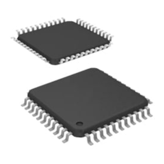
Page 191: 44-Pin Lqfp (10Mm×10Mm) (Fp2.0Mm) Outline Dimensions
BS86DH12C High Voltage Touch A/D Flash MCU with HVIO 44-pin LQFP (10mm×10mm) (FP2.0mm) Outline Dimensions Dimensions in inch Symbol Min. Nom. Max. — 0.472 BSC — — 0.394 BSC — — 0.472 BSC — — 0.394 BSC — — 0.032 BSC —... - Page 192 However, Holtek assumes no responsibility arising from the use of the specifications described. The applications mentioned herein are used solely for the purpose of illustration and Holtek makes no warranty or representation that such applications will be suitable without further modification, nor recommends the use of its products for application that may present a risk to human life due to malfunction or otherwise.
Need help?
Do you have a question about the BS86DH12C and is the answer not in the manual?
Questions and answers